
18
RF-MEMS for smart communication systems and future 5G applications
Abstract
Radio frequency microelectromechanical system(RF-MEMS) technology is suitable for the realization of high-performance reconfigurable wideband radio-frequency passives. The main open issues, i.e., reliability, power handling, packaging, and integration, were effectively addressed across the last 10–15 years, making RF-MEMS technology readiness compatible with commercial applications. From a different perspective, the landscape of 4G-LTE smartphones started to outline the surfacing of performance demands that can be fully addressed by RF-MEMS solutions, i.e., an emerging market-pull rather than technology-push driven scenario. As a result, impedance tuners started to be the first successful commercial exploitation of RF-MEMS technology. Moreover, the upcoming 5G communication standards seem to be the field in which most part of the RF-MEMS value could be extracted. In this chapter, a broad overview on RF-MEMS technology is provided, sketching 15 years of significant achievements reached by the research community, and providing an outlook on future exploitation of such a promising solution.
Keywords
5G; Frequency agility; High-performance RF passives; Microelectromechanical systems (MEMS); Radio frequency (RF); Reconfigurability; RF-MEMS; Tunability; Wideband operability
18.1. Introduction
In 1835, Joseph Henry invented the first electromechanical device, called “switch” or “relay”. It was composed of a bulky electromagnet, which activated an armature able to establish the physical contact of two electrodes. That relay was the brick of the first computer in the late 19th century. The clock speed was limited to tens of hertz, which motivated the well-known extensive use of vacuum tubes, followed by transistors during the 20th century. After several decades of semiconductor foundry developments, complementary metal–oxide semiconductor (CMOS) chips are now drastically reduced in size, operate at GHz frequencies, and consume very low power.
In 1979, Petersen developed the first “micromechanical membrane switches” that was stated to “fill the gap between conventional silicon transistors and mechanical electromagnetic relays” (Petersen, 1975). This was the starting point, opening the route to microelectromechanical systems (MEMS). The key idea, an original concept at that time, was to merge silicon-based microfabrication capabilities with the mechanical relay approach. The proposed MEMS-based switch exploited the electrostatic force applied between a p-doped silicon layer and a bimaterial (SiO2 and gold) membrane to pull down a movable structure and establish an electrical contact (Fig. 18.1(a)). The miniaturization achieved by the microfabrication of such a relay led to envisioning a matrix-addressable cross-point switching array for alternating current (AC) signals. However, the associated maximum operation frequency (200 kHz) was too low to cover radio frequency (RF) or microwave applications.
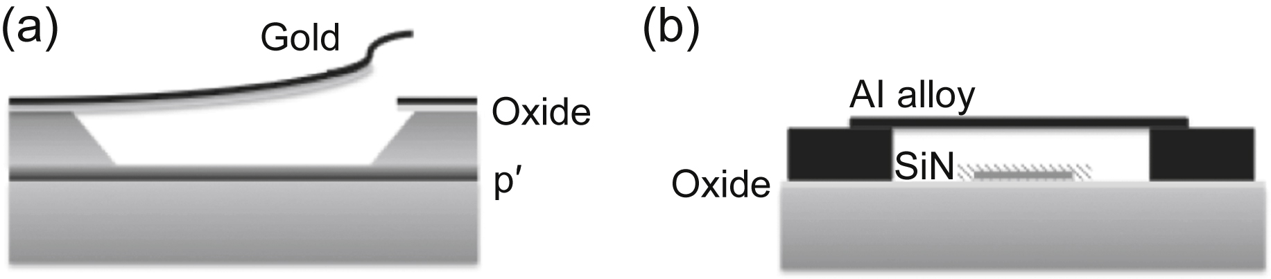
Figure 18.1 Radio frequency microelectromechanical system switches. (a) Petersen (1975) and (b) Goldsmith et al. (1995). (a) From Petersen, K.E., 1975. Micromechanical membrane switches on silicon. IBM Journal of Research Development 23 (4), 376–385. doi: https://doi.org/10.1147/rd.234.0376. Courtesy of International Business Machines Corporation, © International Business Machines Corporation.
During the 1990s, the electrical and microwave community assisted to the appearance of a new class of devices: microrelays capable of processing analog, RF, and microwave signals.
In 1990, Halg introduced the first integrated microelectromechanical nonvolatile memory cell. A year later, Larson et al. (1991) demonstrated a microwave rotating transmission line switch. Measurements performed up to 45 GHz were already impressive with insertion losses lower than −0.5 dB and isolation greater than −35 dB. Years later, in 1995, Goldsmith et al. introduced what was to become one of the best-known bridge configurations for radio frequency microelectromechanical system(RF-MEMS) switches, with a capacitive contact, as illustrated in Fig. 18.1(b). The era of RF-MEMS (i.e., MEMS for RF applications) was then going to emerge (Goldsmith et al., 1996; Pacheco et al., 1998; Muldavin and Rebeiz, 1999; Sovero et al., 1999; Yao et al., 1999; Rebeiz and Muldavin, 2001). After two decades, one can wonder about what potential do MEMS hold for RF and microwave applications, as well as around what are the bottlenecks of such a technology. These crucial points are going to be addressed in the following pages.
18.2. Evolution of RF-MEMS and of market expectations
If we look at all the market forecasts that took turns starting from the early years of 2000s, also bearing in mind the concept of hype curve (Iannacci, 2015a), it seems that the evolution of RF-MEMS experienced two peaks of inflated expectations delayed through time. Providing a straightforward explanation for such fluctuations is not easy. Nonetheless, by analyzing scientific literature, reports, and articles, it is possible to build up a reasonable interpretation. The double peak of inflated expectations and trough of disillusionment can be attributed to two sets of reasons and issues, the first one (around 2004) being predominantly linked to RF-MEMS technology intrinsic factors, whereas the second one (around 2010) being generated by extrinsic circumstances, i.e., not directly linked to the technology itself but rather driven by market needs and acceptance.
The intrinsic factors can be grouped as follows: (1) reliability, (2) packaging, and (3) integration. Right after proving the good performance of RF-MEMS, in terms of high-quality factor (Q-factor), wide tunability, low loss, high isolation, and good linearity, reliability started to emerge as a major issue. Given their multiphysical behavior, MEMS are prone to diverse malfunctioning and failure mechanisms (reversible and irreversible) that are common in material and mechanical engineering, but rather unknown in the community of electronic and RF engineers. Among them, the most important are fatigue, creep, plastic deformation, corrosion, fracture, stiction, and microwelding (Iannacci, 2015b). Therefore, RF-MEMS technology was urging for further development before its exploitation in market applications (DeNatale and Mihailovich, 2003; Lisec et al., 2004; Melle et al., 2003; Rizk et al., 2002).
Linked somehow to reliability, the aspects of packaging and encapsulation caused the initial enthusiasm around RF-MEMS to be reshaped downward. All in all, MEMS devices are very fragile and exposed to harmful environmental factors, such as mechanical shocks, moisture, dust particles, and contaminants. Therefore, they need proper insulation and housing (possibly hermetic or semihermetic) (Jourdain et al., 2003a; Park et al., 2002, 2003). In the specific circumstance of RF-MEMS, the application of a package increases, on one side, the complexity of technology and the manufacturing cost, the latter one being estimated to be as high as 80% of the final product price (Cohn et al., 2002). On the other hand, the presence of additional physical objects, i.e., the package itself, along with the paths for redistribution of electrical signals, spoils the outstanding RF performance of MEMS-based passives. Consequently, the packaging solution must be carefully evaluated, making the design and modeling phases more challenging (Iannacci, 2013a; Iannacci et al., 2006, 2008a; Margomenos and Katehi, 2002, 2003).
Eventually, MEMS technology is typically incompatible with standard semiconductor platforms (e.g., CMOS). Therefore, RF-MEMS in-package passives need to be integrated with active electronics, e.g., through surface mount technologies (SMTs), in order to be properly operated/driven. Ad hoc circuitry must be developed and deployed, as well, to operate them, rising, also in this case, complexity and costs (De Silva and Hughes, 2003; Lu et al., 2005a; Pacheco et al., 2004; Rijks et al., 2003; Zhang et al., 2006; Ziegler et al., 2005). In light of all the just listed challenges, to be faced before getting RF-MEMS ready for market exploitation, the set of reasons causing the drop of expectations mentioned before is sufficiently clear.
Once the scientific community gained consciousness around these issues, plenty of effort was spent after them, thus reducing significantly the gap of RF-MEMS in terms of reliability, encapsulation, and integration/compatibility with standard semiconductor active technologies, and boosting, as a result, expectations and optimism at market-level for the years to come (Iannacci, 2015a). Nevertheless, struggle for RF-MEMS was not over, yet, when technology gained proper maturity, toward the end of the first decade of 2000s.
The second trough of disillusionment of RF-MEMS can be mainly attributed to factors extrinsic to technology (i.e., market-related). In 2001, Nguyen provided an inspiring overview of how RF-MEMS technology could have been exploited during the upcoming (at that time) years in the mobile handsets market. The superheterodyne transmitter/receiver (transceiver) architecture was taken as reference. The first commercial exploitation of RF-MEMS technology, according to his forecast, was supposed to be the replacement of low-complexity elements (e.g., switches and LC-tanks) in standard technology, with their microsystem-based counterparts.
The remarkable characteristics of RF-MEMS components, such as low loss, high Q-factor, etc., were expected to improve the performance of the whole receiver. Thereafter, Nguyen elaborated a more visionary and extensive exploitation of RF-MEMS technology, as well. In the latter context, the architecture of the entire receiver was supposed to be rethought based on RF-MEMS (Iannacci, 2015a). High-complexity RF-MEMS blocks were supposed to replace entire portions of the receiver, thus reducing hardware redundancy and need for amplification stages, in light of the very low losses enabled by microsystem-based elements. This sort of revolution was envisaged not only to boost the performance of the entire receiver but also to extend significantly its reconfigurability, making the same hardware operable according to different and heterogeneous telecommunication standards and services (e.g., GSM, WLAN, and so on).
Despite the enlightenment of Nguyen's vision, market needs and especially the constraints it imposes impaired its turning into reality. Since their wide diffusion in the second half of the 1990s, mobile phones, as a matter of fact, used to work pretty well. The perspective of replacing small transceiver blocks with more expensive RF-MEMS devices, also giving rise to problems at integration level, just to improve a little performance of handsets could not be successful according to market philosophy and drivers. This caused the second trough of disillusionment (Iannacci, 2015a) that commenced to be interpreted also as the possible final defeat of RF-MEMS technology in the mass-market arena.
Surprisingly enough, recent development of the large market of smartphones seems to be nurturing once again hope for successful commercial exploitations of RF-MEMS technology. Since the widespread diffusion of mobile phones in mid-1990s, voice signal quality has been experiencing a degradation trend, hopping from one generation to the next one (i.e., GSM, 2.5G, and so on) (Allan, 2003). As smartphones become smaller and thinner, it is difficult to integrate proper circuitry to boost performance, counteract dropped calls, and improve voice quality. It is estimated that the ratio of theoretical versus actual RF signal quality has been decreasing with a pace of about 1 dB per year for over a decade (Allan, 2003). Because of all these factors, antennas of most of today's smartphones do not work efficiently, leading to slower download speeds, reduced quality of voice, lower energy efficiency, and more dropped calls (Jacobs School of Engineering, 2014). Given such a scenario, the characteristics of high-performance and wide reconfigurability belonging to RF-MEMS are now very attractive for commercial applications. Nonetheless, having in mind the history of MEMS technology for RF passives in the last 10–15 years described above, one could reasonably be skeptical and wonder if this is simply another evanescent peak of expectation that soon will reverse its momentum.
To this regard, it should be kept in mind that there is a substantial difference in the smartphones market of today if compared to the early days of RF-MEMS. Although in the first years of the 2000s, despite the soundness of the vision of Nguyen discussed above, there was not a factual need for RF passives with better performance; on the other hand, nowadays the availability of such components can make the difference. In other words, if the early approach to the commercial exploitation of RF-MEMS was mainly technology-push based, today it is turning into a market-driven scenario (Martin, 1994). Very likely, such a metamorphosis of the surrounding context already commenced to draw the line between the lacking and the successful affirmation of RF-MEMS technology in mass-market applications.
One of the first needs to be addressed, as suggested by the decreasing trend discussed by Allan (2003), is to improve the quality of connection in modern smartphones. As stated above, demands for compact and within-device integrated antennas have decreased the efficiency and made them more sensitive to interaction with external items, such as speaker's head or hand holding the handset. Therefore, a fixed impedance matching between the antenna and the RF front-end (RFFE) is not anymore an optimal solution, as the characteristic impedance of the transmitting/receiving aerial undergoes slight changes. Availability of high-performance reconfigurable impedance matching tuners started to be desirable, and RF-MEMS is demonstrating to be the proper technology solution to realize such complex devices. To this regard, in 2012 the presence of RF-MEMS-based adaptable impedance tuners manufactured by WiSpry Inc. (wispry.com) within Samsung's Focus Flash Windows smartphone was announced (IHS iSuppli, 2012). More recently, in fall 2014, Cavendish Kinetics B.V. (cavendish-kinetics.com) announced the commercial adoption of their RF-MEMS-based SmarTune antenna tuning solution in the Nubia Z7 smartphone, manufactured by the Chinese ZTE Corporation (Cavendish Kinetics, Nubia Adopts, 2014). Few months later, Cavendish Kinetics went public with the information that SmarTune products were adopted in five different Chinese smartphone models, promising signal enhancement of 2–3 dB, resulting in boosted data rates (up to 2×) and improved battery life (up to 40%) (Cavendish Kinetics adds design, 2015).
In conclusion, diverse signals suggesting a robust market acceptance of RF-MEMS technology have been growing stronger in very recent years, finally making envisage concrete exploitation perspectives for microsystem-based RF passives. Coming back for a moment to the vision of Nguyen (2001), it seems that it is somehow taking place, despite according to a reversal development. The first market exploitation of RF-MEMS technology is related to complex reconfigurable networks (i.e., impedance tuners at first), which was supposed to be phase two of microsystem RF components. Spreading of such networks is increasing the demand for high performance, reliable, and low-cost basic RF-MEMS components (mainly switches and tunable capacitors), thus pushing advanced research and engineering of such building blocks, as well.
18.3. RF-MEMS in the emerging 5G scenario
The emerging world of 5G appears to be a field of convergence for diverse demands and challenging requirements as rarely the research and industrial community witnessed before. After all, since the massive diffusion of mobile handsets roughly two decades ago, the trend to integration of more wireless services supported by the same device was relentless. To this regard, 5G systems are predicted to deliver up to 1000 times the capacity of current mobile networks (Baldemair et al., 2015). Broadband wireless applications, such as high-resolution video streaming and Tactile Internet (Dohler, 2015) will urge for data rates that could be 10–100 times wider compared with the 4G networks operating today (Fettweis, 2014; Osseiran et al., 2014).
On a different level, the Internet of Things (IoT) paradigm portrays an ongoing technology development path, through which any object and environment belonging to our daily life experience, earns its own identity in the digital world, by means of the Internet (Internet of Things, 2016; Uckelmann et al., 2011). Given the IoT frame of reference, 5G mobile systems are expected to accommodate a wider range of wireless connections, supporting emerging applications such as machine-to-machine, and, in turn, all the more stringent requirements they bring, in terms of quality of service (QoS), concerning reliability, spectral and energy efficiency, and so on (Wu et al., 2011; Bhushan et al., 2014; Boccardi et al., 2014).
Give such premises, it is straightforward that there will be no unique enabling technology capable of addressing all the challenging (and often conflicting) requirements of next-generation 5G applications (Le et al., 2015). Innovation and reengineering of network architectures and algorithms will be necessary. This, of course, will demand both for novel hardware and software solutions. Just to mention some of the existing limitations that will have to be overcome at architectural and implementation level, the currently in use orthogonal frequency multiple access waveform (exploited in 4G applications) will need to be replaced by more efficient solutions. Moreover, network diversification, employment of large-scale multiple-input multiple-output units, and use of millimeter Wave- (mmW-) spectrum to ensure gigabit (Gb) communications, will have to be ventured (Le et al., 2015).
Bearing in mind the previously discussed market-pull scenario that started making RF-MEMS solutions successful (up to now for impedance matching tuners), it is envisaged that 5G communication protocols will demand for higher operation frequencies (e.g., well above 6 GHz) and large reconfigurability to cover different services, while reducing hardware redundancy and power consumption. To target these challenges, it is necessary to leverage on passives with boosted characteristics (low loss, high isolation, etc.), and RF-MEMS technology is indicated as one of the most promising candidates, both for what concerns 5G smartphones (i.e., RFFEs) and base stations (Lapedus, 2015).
From a different perspective, regardless of the specific technology employed, RF components always need to be packaged and integrated into more complex subsystems and systems. If, on one side, the primary role of the package is to protect devices from potentially harmful (environmental) factors (Jin et al., 2010), it has been realizing, on the other hand, more and more functionalities (Kuang et al., 2010). As a matter of fact, the massive growth of RF systems for mobile communication taking place since years has been driving miniaturization, high-integration density, and low-cost fabrication solutions.
Nowadays, RF systems-on-chip employ hundreds of passive components and only few tens of integrated circuits (ICs) (Cost-Effective (WL-IPD), 2014). Given that such components are often manufactured in diverse, incompatible, and nonmonolithic technologies, it is easy to understand that their successful integration can only take place through high-performance and high-density wafer-level packaging (WLP) solutions. Of course, designing and realizing a package that ensures high-reliability (Iannacci, 2015b), high-density integration and very-low impact on the performance of RF passive (MEMS and non-MEMS) components (Iannacci et al., 2008a; Lahti et al., 2013) is a rather challenging task. This is the reason why, as mentioned above, the packaging/integration phase, in some cases can be more expensive than the realization of the actual RF components to be packaged. Nonetheless, in spite of all the existing challenges to be addressed, it is clear that driving trends of future developments are oriented along the direction of integration of heterogeneous technologies, leaving monolithic manufacturing of functional RF blocks and subsystems within the same technology platform, to the cases in which the achieved performance enhancement is very critical for the specific application.
18.4. RF-MEMS technology: a general overview
RF-MEMS technology concepts rely on bulk and surface micromachining techniques, which have already proven their potentialities in high-volume commercial applications, such as micromirrors in video projectors, inkjet printers' heads, as well as, in more general terms, for integrated sensors (e.g., accelerometers) and actuators.
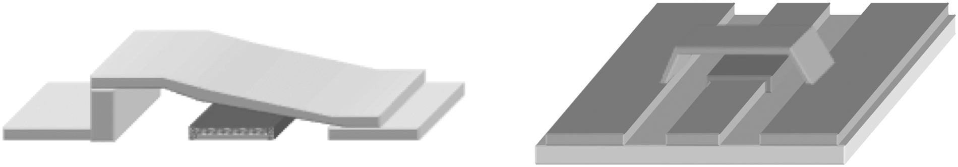
Tunable RF-MEMS devices typically employ bridge or cantilever configurations, as shown in Fig. 18.2. Regardless of the specific topology, the movable membrane exhibits a vertical movement during actuation. Some RF-MEMS may exploit lateral movement, like the switch developed by Oberhammer et al. (2006), which involves the superposition of two bonded substrates (silicon and glass wafers). The top silicon substrate is dry etched to realize the movable component, whereas the bottom glass wafer is wet etched to allow the free movement of the metalized silicon beam.
Different actuation mechanisms have also been studied, despite most of RF-MEMS architectures rely on electrostatic control because of its easy integration in the fabrication process and of low-power (virtually zero) consumption. Nevertheless, for some specific applications and sets of requirements, thermoelectric (Daneshmand et al., 2009), piezoelectric (Kawakubo et al., 2005), and electromagnetic (Cho et al., 2005) actuation mechanisms may also be encountered, each of which presenting specific advantages and drawbacks.
In the following two sections, we will provide a broad overview around the wide variety of passive components that can be realized in RF-MEMS technology, as well as of the different increasing complexity, at topology and functional level, that can be addressed. To simplify the report of the selected representative case studies, we focus exclusively on electrostatically driven MEMS switching/reconfiguring units. Moreover, we refer to two main technology platforms, namely, one suitable for the realization of capacitive microdevices, i.e., tunable capacitors (varactors) and switched (ON/OFF digital) capacitors, and another one, more flexible from the design point of view, that enables also the realization of ohmic devices, i.e., metal-to-metal contact switches and switching units.
18.5. RF-MEMS technology for capacitive microdevices
Numerous RF-MEMS device architectures may be found in literature and Rebeiz (2003) provides comprehensive overview. Here the focus is spent around the devices introduced by Goldsmith et al. (1995), in which a mechanical bridge is moved up and down over a coplanar waveguide (CPW) due to the electrostatic attraction force. When the metallic bridge is down, it contacts a thin dielectric layer that prevents ohmic DC contact with the line. Such a type of contact is addressed as “capacitive” in contrast with the ohmic one, when one metal established physical contact with another one. For this configuration, the process flow is globally divided in five main steps, as illustrated in Fig. 18.3 and reported in Grenier et al. (2004, 2005).
The first step consists in defining the RF transmission line, which is sketched with a CPW. In the case of capacitive switches, a dielectric layer is then deposited and patterned on the lines (see Fig. 18.3(b)). The next step is the definition of a sacrificial layer (see Fig. 18.3(c)), which will support the movable membrane during its fabrication (see Fig. 18.3(d)). Finally, the sacrificial layer is removed to release the RF-MEMS structure.
By means of this technology, it is possible to integrate with both microwave passive and active circuits, high-performance switches, and variable capacitors (i.e., varactors). Before giving some examples of architectures in which RF-MEMS devices bring real added value, let us examine the performances achievable by such devices.
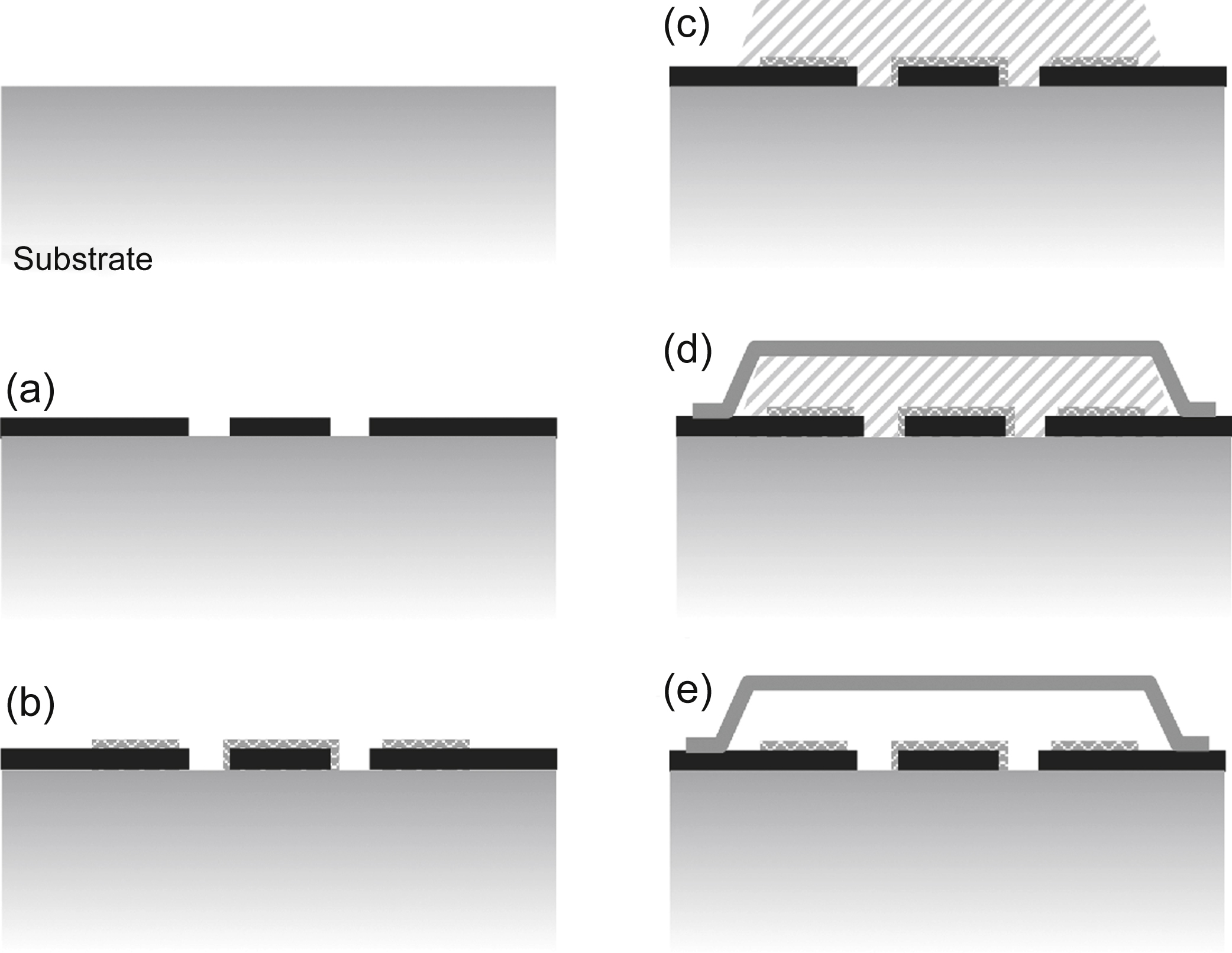

Fig. 18.4(a) presents high-isolation X-band MEMS capacitive switch (Tang et al., 2005). The pull-down voltage has been optimized around 20 V with the use of serpentine folded low-effective spring constant suspensions. Even if this value is rather high compared with the 3.3–1.8 V used for CMOS devices, it is a good compromise between low-operating voltage and high-degree of reliability. Charge pump circuits may also be associated with RF-MEMS devices, to operate even in presence of low voltages. This is a minor drawback with respect to the high level of achievable microwave performance. Insertion losses of −0.1/−0.35 dB and isolation of −16.5/−28 dB are measured for the device presented in Fig. 18.4(a), which show a clear improvement compared to solid-state switches (Rebeiz, 2003). Fig. 18.5 illustrates the operation of such capacitive RF-MEMS switches. The movable metallic membrane defines, together with the coplanar line underneath, a variable capacitor realizing low capacitance when the membrane is up, and high capacitance when the membrane is in contact with the underlying dielectric. A low value of the off-state capacitor ensures a low-loss operation, as well as high on-state capacitance allows to achieve high performance in terms of isolation.
Similar devices are presented in Fig. 18.4(b) and have been characterized from 1 up to 40 GHz (Grenier et al., 2005). The main results consist in an insertion loss better than −0.2 dB up to 20 GHz (including the CPW ports) and isolation better than −15 dB from 10 up to 40 GHz. The upstate (Cup) and downstate (Cdown) capacitances with values of 65 fF and 2 pF, respectively, were extracted from the measurements. It must be pointed out that the Cdown/Cup ratio exhibits a value of 30, which is sufficient to ensure good operation of the device as switch.
The capacitive RF-MEMS device shown in Fig. 18.4(b) has been developed through a low-loss technology compatible with above-ICs integration (Grenier et al., 2005). It consists of a 3 μm-high gold membrane and a 0.25 μm-thick silicon nitride (SiN)-based dielectric. It has to be noted that the attracting electrodes are decoupled from the RF signal to facilitate the mechanical, electromechanical, and microwave design (Ducarouge et al., 2004). It should also be highlighted that this translates into a longer membrane that demands for specific anchor design, to ensure the high quality of the contact.
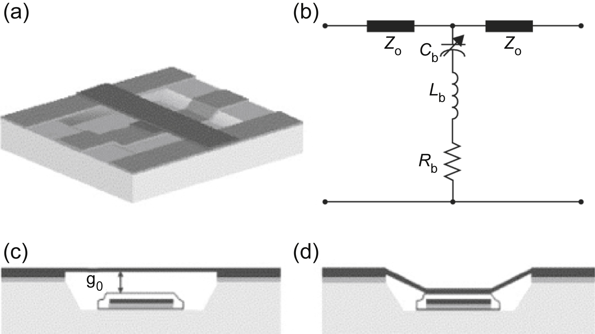
Figure 18.5 Radio frequency microelectromechanical system capacitive switches. (a) Typical schematic, (b) equivalent electrical model, (c) cross-sectional view in the upstate and (d) downstate. Reproduced from Tang, M., Yu, A.B., Liu, A.Q., Agarwal, A., Aditya, S., Liu, Z.S., 2005. High isolation X-band MEMS capacitive switches. Elsevier. Sensors and Actuators A: Physical 120 (1), 241–248. https://doi.org/10.1016/j.sna.2004.11.026.
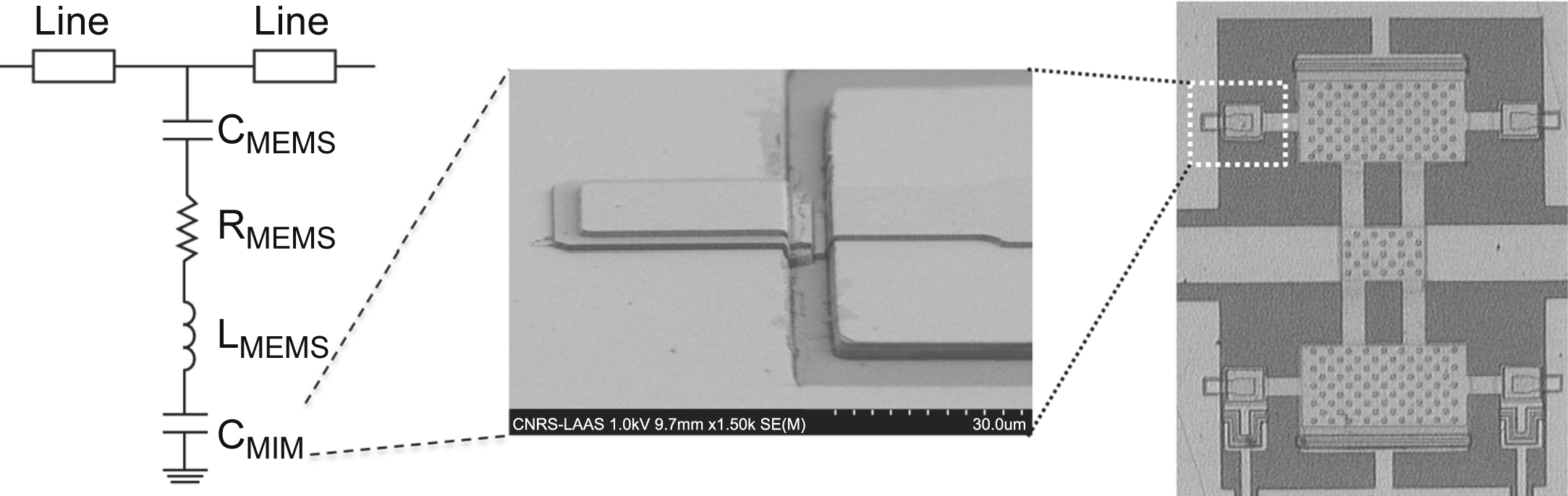
Figure 18.6 Radio frequency microelectromechanical system capacitive varactor. MEMS, microelectromechanical system; MIM, metal-insulator-metal.
As far as the systems tunability is concerned, varactors featuring a capacitive ratio in the range of 2–5:1 are also required (together with RF-MEMS switches) (Shen and Barker, 2005). Consequently, new MEMS configurations that integrate a constant metal–insulator–metal (MIM) capacitor have been developed, as presented in Fig. 18.6. The idea is as simple as efficient. Adding a fixed capacitor in series with the MEMS capacitor tends to reduce the resulting range of the total capacitance, as well as, in turn, the ratio.
The technology process flow depicted in Fig. 18.3 has been modified to integrate such MIM capacitors. Two additional steps are required. After the realization of the RF lines, the MIM dielectric (in SiN) is deposited by plasma-enhanced chemical vapor deposition (PECVD) and then patterned. A top metallization is realized by evaporation and is patterned to define the top electrode of the fixed capacitor. The MEMS process restarts then with the deposition of the dielectric and continues until the final release of the structure. Because of certain limitations at technology level, MIM capacitors have to present a value in the range of 100–200 fF. The MIM capacitor value corresponds to few hundreds fF, which leads to varactor values (MEMS and MIM capacitors in series configuration) of ∼100 and ∼500 fF in the up- and downstate, respectively. This results in a capacitive ratio from 2 to 5 (Bordas et al., 2007).
Vähä-Heikkilä proposed another solution based on metal–air–metal (MAM) capacitors with RF-MEMS. It leads to higher (Q-factor), as no dielectric losses appear in the MAM device. A 150% improvement in the off-state Q-factor, which presents a value of 154, was obtained at 20 GHz (Vähä-Heikkilä and Rebeiz, 2004).
18.6. RF-MEMS technology for ohmic microdevices
The possibility of having direct metal-to-metal, i.e., ohmic, contact opens up the floor to a significantly wide variety of other devices and functions/functionalities, which can be addressed and implemented in RF-MEMS technology. This, however, implies modifications at technology level and extension of the fabrication process flow, as, differently from the case of capacitive devices, direct contact between RF signals and DC biasing must be avoided. In other words, as far as the electrostatic pull-in of RF-MEMS switching elements is concerned, an additional and insulated layer is necessary to act as biasing fixed counter electrode with respect to the movable membrane and drive, therefore, its actuation. To this regard, a suitable example of RF-MEMS flexible technology platform, able to be extended to realize both capacitive and ohmic devices, is the one available at the Center for Materials and Microsystems (CMM) of Fondazione Bruno Kessler (FBK), briefly addressed as CMM-FBK, in Italy. The technology is based on surface micromachining of 6-inch silicon wafers (Giacomozzi et al., 2011; Giacomozzi and Iannacci, 2013), and the schematic representation of the process flow is reported in Fig. 18.7.
Such a solution employs two buried conductive layers, i.e., high-resistivity polycrystalline silicon (poly-Si) for DC biasing lines and electrodes (Fig. 18.7(a)) and low-resistivity aluminum layer for RF signal underpasses (Fig. 18.7(b)). Then, a thin gold-evaporated metallization is deposited above the contact areas (Fig. 18.7(c)) to ensure good metal-to-metal contact with the above MEMS structural parts (still to be processed). Subsequently, the actual realization of suspended membranes and RF transmission lines is performed. A first electroplated gold metallization (around 1.8 μm thick, reported in Fig. 18.7(d)) defines the MEMS structures, as well as the air gaps, wherever a photoresist sacrificial layer is patterned. A second gold electrodeposition (around 3 μm thick, reported in Fig. 18.7(e)) defines the device areas that are supposed to be more stiff and robust, such as the anchoring parts for suspended membranes, the surrounding CPW frames, and so on. Finally, removal of sacrificial layer releases the suspended MEMS parts (Fig. 18.7(f)), that from that moment on, can be operated by applying suitable DC biasing signals.
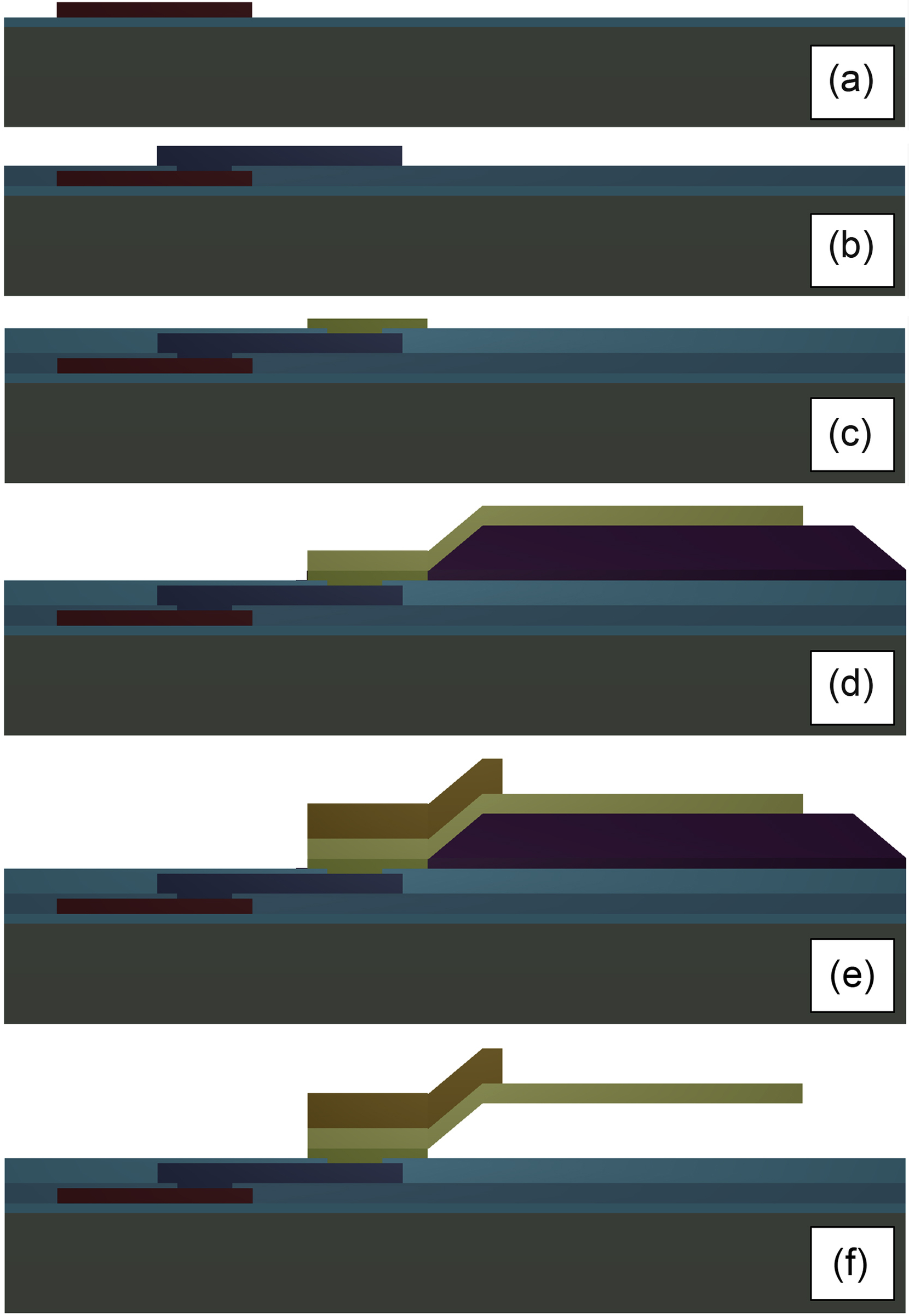
Figure 18.7 Schematic cross-section of the radio frequency microelectromechanical system surface micromachining process available at Center for Materials and Microsystems of Fondazione Bruno Kessler, in Italy. (a) Patterning of poly-Si, (b) patterning of aluminium layer, (c) evaporation of gold, (d) electrodeposition of the 1st gold layer, (e) electrodeposition of the 2nd gold layer, (f) release of MEMS suspended structures.
Leveraging on such a technology solution, it is possible to realize electrostatically controlled series ohmic microrelays, like the one depicted in Fig. 18.8, with very good characteristics in terms of low resistance when ON (leading to low loss of RF signal) and low parasitic capacitive coupling when OFF (enabling very good isolation) (Iannacci et al., 2010a; Seki et al., 2013; Moon et al., 2014; Liu et al., 2014). Moreover, ohmic contact boosts wideband operability of RF-MEMS microswitches, covering very large frequency spans, ranging from DC up to 50–60 GHz and more.
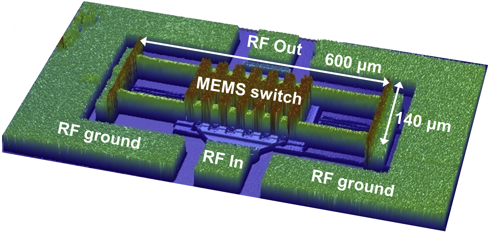
The image in Fig. 18.8 shows the 3D topology of a series RF-MEMS ohmic switch realized in the CMM-FBK technology, acquired with an optical profiling system (based on interferometry). The device is composed by a central elevated MEMS membrane, whose small dimensions are labeled in figure, surrounded by a CPW frame. The former is suspended above interdigitated poly-Si actuation electrodes, schematically reported in Fig. 18.9(a), whereas the input/output RF terminations, implemented in the aluminum layer (Fig. 18.9(b)), are interrupted. Therefore, when the MEMS membrane is in the rest position, the microswitch is OFF and isolates the input/output branches. Differently, when the membrane is biased and pulled in, the microrelay is ON and connects the two RF terminals.
Starting from such a simple device concept, it is possible to realize more complex functions and devices with multiple configurations, simply duplicating the number of microrelays and the way they are deployed and connected on the RF line. Some of such higher-order networks are discussed in Iannacci et al. (2012), Figur et al. (2012), Shah et al. (2016) and Iannacci (2013b), and a few of them will be discussed into more details in the following section.
18.7. RF-MEMS-based circuits for smart communication systems
Based on a wide portfolio of RF-MEMS devices, high-performance reconfigurable microwave systems can be envisioned. RF-MEMS devices may, indeed, be added directly to passive functions (e.g., filters, matching network, etc.) with no compromises in performance. Basically, there are two ways of bringing smartness to circuits: (1) Improve circuit tunability through switches and varactors (Fig. 18.10(a)); (2) Enable commutation between two circuits, i.e., between two RF paths, as illustrated in Fig. 18.10(b).
In the case of Fig. 18.10(b), the commutation between paths 1 and 2 is performed with two RF-MEMS-based single-pole double-throw (SPDT) switches (Pacheco et al., 2001). Paths 1 and 2 may correspond to two filters featuring different central frequencies or two power amplifiers (PAs) with distinct nominal operating power. Fig. 18.11 presents an RF-MEMS SPDT switch. The SPDT structure comprises two MEMS parallel switches, which enable selection of the active channel, and two quarter-wave impedance inverters meant to transform the RF short wave emitted by the MEMS switches into an open circuit and virtually cancel the presence of the inactive channel (Dubuc et al., 2003). High performances are achieved: only −0.6 dB of insertion losses is measured at 30 GHz, whereas isolation is expected to reach −30 dB. Higher isolation can be reached by cascading RF-MEMS switched as illustrated in Fig. 18.12 (Tang et al., 2005). A 7 dB improvement in the X-band has been measured compared with a single-MEMS switch. This improvement translates into an increase of only 0.3 dB in insertion losses. An example of more complex switching unit is reported in Iannacci et al. (2012). It is a single-pole four-throw (SP4T), which exploits double-cascaded series/shunt ohmic microrelays, to improve the performance in terms of isolation, when a channel is not conducting. Basically, a series ohmic switch, when ON (i.e., pulled-in), ensures the connection of a certain branch with very limited loss, better than −1.2 dB up to 40 GHz. On the other hand, when the switch is OFF, the small series residual capacitance of the floating suspended membrane over the fixed electrode can induce slight worsening of isolation. To this regard, when the series ohmic switch is OFF, a paired shunt-to-RF ground ohmic switch can be activated, thus realizing a short that cuts out possible cross talk between the OFF branch and the other ones. Measured S-parameters show that isolation (S21) between two nonconnected SP4T terminations is better than −40 dB up to 20 GHz and of −25 dB up to 40 GHz (Iannacci et al., 2012).

Figure 18.9 Schematic of the buried layers deployed underneath the MEMS switch in Fig. 18.8. (a) Poly-Si exploited for the DC biasing of the movable membrane, and (b) aluminum layer used for the input/output RF interconnections. Poly-Si, polycrystalline silicon; RF, radio frequency.
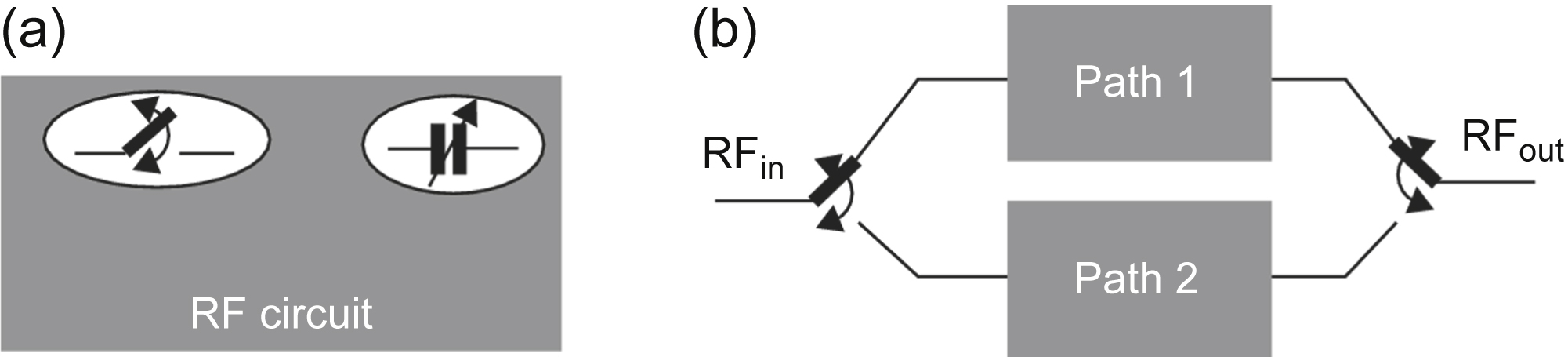
Figure 18.10 Radio frequency microelectromechanical system–based smart microsystems. (a) With tunable devices and (b) with switchable circuits.

Figure 18.11 Radio frequency microelectromechanical system (RF-MEMS)-based single-pole double throw.

Figure 18.12 Radio frequency microelectromechanical system–based high-isolation switch. Reproduced from Tang, M., Yu, A.B., Liu, A.Q., Agarwal, A., Aditya, S., Liu, Z.S., 2005. High isolation X-band MEMS capacitive switches. Elsevier. Sensors and Actuators A: Physical 120 (1), 241–248. https://doi.org/10.1016/j.sna.2004.11.026.
The circuit architectures depicted in Fig. 18.10(a) cover a very wide range of topologies. Two of them, probably the most generic ones, relate to impedance tuners and phase shifters. The former ones can be used for the intelligent control of the optimum operation of a PA over various frequencies (Qiao et al., 2005).
An implementation of multistate impedance matching tuner in RF-MEMS technology is discussed in Iannacci et al. (2011a). The microphotograph of the fabricated sample is reported in Fig. 18.13. The device comprises eight-cascaded reconfigurable stages, thus enabling 256 different impedance configurations between the input and output ports. A bank of eight coils (air-suspended inductors) is visible in the top part of the device, whereas eight MIM capacitors are visible in the bottom part. Both the just mentioned reactive components are alternatively configured in series and shunt with respect to the RF line and can be inserted or deselected by means of ohmic switches, also visible in figure. The whole device realizes a double LC-ladder configuration, where each element of the in-line and shunt branches can be capacitive, inductive, both in parallel or simply a short (for the series elements), or open (for the shunt elements). The network realizes 256 different impedance configurations and can work on a rather wide frequency range, up to 30 GHz (Iannacci et al., 2011a).

Figure 18.13 Microphotograph of the multistate 8-bit reconfigurable impedance matching tuner in radio frequency microelectromechanical system technology, discussed in Iannacci et al. (2011a).
Still keeping the focus on RF-MEMS-based impedance tuners, an example of hybridization of different technologies (i.e., RF-MEMS and CMOS) is reported in Larcher et al. (2009). The passive impedance tuner layout is shown in Fig. 18.14(a), the lumped-element network is reported in Fig. 18.14(b), while more details about it are available in Iannacci et al. (2008b). It consists of three ¾-a-circle planar inductors and shunt MIM capacitors. Two MEMS ohmic microrelays control the insertion/shorting on the RF line of a series and of a shunt capacitor, thus implementing the required impedance transformation from 12 to 50 Ω in both the GSM operation frequency bands, i.e., 900 MHz and 1.8 GHz.
Other implementations in RF-MEMS technology of reconfigurable impedance matching tuners are available in literature. Some of them are discussed in Festo et al. (2009), Morris et al. (2012), Figur et al. (2013), Sharma and Gupta (2014).
Fig. 18.15(a) depicts another implementation of 6-bit impedance tuner operating at 20 GHz. The measurements demonstrate that the tuner is able to match impedance values as low as 20 up to 100 Ω. The corresponding impedance matching ratio of 5:1 is interesting for a wide range of applications, where low noise amplifiers (LNAs) or PAs and antennas have to be matched under different frequency ranges. The impedance tuner is, then, a key building block for reconfigurable microwave circuits, where impedance matching in various switchable conditions is mandatory.
Figure 18.14 (a) Layout of the radio frequency microelectromechanical system impedance matching tuner for the class-E GSM power amplifier discussed in Iannacci et al. (2008b). (b) Equivalent lumped-element network.
A true time delay (TTD) phase shifter is presented in Fig. 18.15(b). It corresponds to MEMS-based switchable capacitors periodically distributed over a CPW (Palei et al., 2005). Low-insertion losses (−2.3 dB) for a large phase shift (250 degrees) with a low-return loss (−15 dB) has been demonstrated up to the Ku-band. Such remarkable characteristics, enabled by RF-MEMS technology, permit the envisioning of clear performance enhancements in radar and telecommunication systems. Beam steering is probably one of the main applications, for which such circuits may boost breakthrough performances.
The integration of RF-MEMS switches over radiating elements has also been considered to achieve smart antennas. Fig. 18.16 presents a rectangular patch antenna with a tunable operating frequency, for which MEMS technology is expected to ensure high antenna efficiency. A 1 GHz tunability of the antenna resonant frequency has been achieved in the X-band (Topalli et al., 2009), with no alteration of the radiation pattern. Such a tunable antenna is one of the critical elements for smart telecommunication systems, to maintain various operating frequencies (i.e., more functionalities) with a single antenna unit (low volume and cost).
Reconfigurable filters also benefit from RF-MEMS capabilities (through low losses, notably). A 10% frequency tuning range is demonstrated in the X-band (Bouyge et al., 2012), which is attractive for the selection of various wireless communication standards with a single reconfigurable filter. Fig. 18.17 illustrates such a filter based on a split ring resonator in association with eight RF-MEMS switches. The reported RF-MEMS switches and varactors exploited to bring reconfigurability, tunability, or smartness to microwave systems are just a few examples among many others, featuring a certain degree of agility (in terms of covered standards, operating frequency, operating power, etc.) (Kim et al., 2001; Lu et al., 2003; Fukuda et al., 2004; Hacker et al., 2004; De Graauw et al., 2006; Liu et al., 2011; Rantakari et al., 2011; Fouladi et al., 2012).
Another example of bandpass filter, entirely based on RF-MEMS technology and operating in the Ku-band, is discussed in Contreras et al. (2014, 2013). In this case, RF-MEMS ohmic air bridges reconfigure the reactive loading on the line, thus modifying the bandpass for center frequencies around 12–13 and 18 GHz, respectively, and causing losses of just a few dB.

Figure 18.16 Radio frequency microelectromechanical system–based tunable dual-frequency antenna. Reproduced from Topalli, K., Erdil, E., Civi, O.A., Demir, S., Koc, S., Akin, T., 2009. Tunable dual-frequency RF MEMS rectangular slot ring antenna. Elsevier. Sensors and Actuators A: Physical 156 (2), 373–380. https://doi.org/10.1016/j.sna.2009.10.005.
Figure 18.17 Radio frequency microelectromechanical system (RF-MEMS)-based tunable filter. (a) Filter topology and (b) RF-MEMS switches architecture. Reproduced from Bouyge, D., Crunteanu, A., Durán-Sindreu, M., Pothier, A., Blondy, P., Bonachel, J., Orlianges, J-C., Martin, F., 2012. Reconfigurable split rings based on MEMS switches and their application to tunable filters. IOP. Journal of Optics 14 (11), 1–9. http://iopscience.iop.org/2040-8986/14/11/114001.
Additional valuable contributions devoted to the implementation of bandpass reconfigurable filters in RF-MEMS technology are available in Chaabane et al. (2014), Li et al. (2015), Hickle et al. (2016) and Chan et al. (2017).
A different class of passives that can be effectively implemented in RF-MEMS technology is that of the RF power attenuators. This type of component, basically, exploits resistive loads, which can be deployed in series or shunt configuration on the RF line, to attenuate the amplitude of the signal traveling through the device. The feature of reconfigurability is obtained by means of MEMS ohmic switches, which can indeed insert/short resistive loads in series and select/deselect shunt resistive loads, thus varying the total amount of resistance and, in turn, the targeted attenuation level.
The first examples of higher-order multistate reconfigurable RF power attenuators in MEMS technology were tested up to 30 GHz, as reported in Iannacci et al. (2009). More recently, improved design concepts of RF-MEMS attenuators were reported in literature, leading to significant improvements of the device characteristics in terms, not only of realized attenuation levels but also of voltage standing wave ratio and, therefore, of reflected power (Sun et al., 2016; Guo et al., 2016). To this regard, a very recent work demonstrates RF-MEMS basic attenuator modules (i.e., ON/OFF building blocks) in series and shunt configuration, working from nearly DC up to 110 GHz (Iannacci et al., 2016). Attenuator modules are realized in the CMM-FBK technology (Iannacci, 2013a), previously discussed in Fig. 18.7, and employ buried poly-Si resistors. The modules exhibit attenuation levels in the range from −5 to −10 dB, from 10 MHz up to 110 GHz, with flatness of 2–3 dB from 10 MHz to 50 GHz, and of about 2 dB from 60 up to 110 GHz. When OFF, the attenuator modules introduce loss (S21) better than −1 dB up to 50 GHz and better than −6 dB up to 110 GHz.
From the perspective of industrial applications, additionally, another important issue is dealing with the reliability and the robustness of the different modules. They have to feature certain repairing and/or tuning functionalities to guarantee high QoS, as it will be discussed more in details in the following pages.
The RF-MEMS added value, i.e., the high level of performance and large-scale integration in microsystems for smart communication systems needs to be achieved without jeopardizing reliability. This is crucial, especially if we consider commercial applications. The next two sections are going to address the issues of reliability and the power capabilities of RF-MEMS devices.
18.8. RF-MEMS reliability
It is well known that the main cause of failure in RF-MEMS devices is due to dielectric charging, which causes stiction (van Spengen et al., 2002; Yuan et al., 2004; Melle et al., 2005) of the mobile membrane over the coplanar line, i.e., the missed release of the device when the DC bias is removed. The dielectric layer on top of the line then plays a central role in the reliability of capacitive RF-MEMS. Various dielectric materials are available, and the required thickness is generally in the order of 0.2 μm, which allows the use of both polymer and mineral layers. The use of polymers may be possible, but their nonconformal deposition and their low permittivity make mineral dielectrics better candidates. Dielectric layers such as SiO2 or SiN, obtained by PECVD, are preferred because their low-thermal budget is compatible with the metal of the transmission lines and also with possible active circuits located underneath. Their fabrication process subsequent to deposition, traditionally involves reactive ion etching using a photoresist mask. To simplify the understanding of the global process, the dielectric layer in Fig. 18.3(b) is realized on top of the transmission line, prior to the sacrificial layer deposition. As this layer is present to avoid any direct contact between the transmitted signal line and the movable membrane, it may also be processed during the formation of the tunable part of the MEMS element.
The physical phenomenon linked to charge accumulation is the undesired stiction, i.e., the missed release of the MEMS movable part even when the DC bias is removed. This occurs because when the voltage is applied to actuate the bridge or cantilever, charges accumulate within the dielectric and yield to the presence of a residual bias. If such a spurious voltage is larger than the pull-out (i.e., release voltage) of the MEMS device, the latter one remains pulled-in even without any applied DC bias (Iannacci, 2015b). Apart from stiction, charge accumulation in the dielectric affects nominal operation of MEMS also in other ways. Indeed, the unwanted residual bias, even if not large enough to keep the MEMS pulled-in, screens the actual DC bias applied to operate the movable device(i.e., voltage screening phenomenon), thus inducing nonnegligible shifts of the nominal pull-in/pull-out voltage (Iannacci, 2015b). This effect is illustrated in Fig. 18.18.
To overcome this problem, several solutions have been investigated. One consists in replacing the dielectric layer with air. To avoid any contact between the membrane and the transmission line during actuation, dimples are placed on the movable membrane in front of the slots in the bottom metallic layer (Mardivirin et al., 2008, 2009; Fall et al., 2013; Tazzoli et al., 2010).

Another investigation looked into doping the dielectric layer, to facilitate the evacuation of the charge during the application of the electrostatic force. This may be achieved by doping a SiN layer with Si, as patented by Ehmke et al. (2002). It may also be achieved by the incorporation of carbon nanotubes (CNTs) in the dielectric layer (Bordas et al., 2007). CNT doping translates into several orders of magnitude in improvement of the MEMS life span.
When dealing with ohmic contact-based RF-MEMS microrelays, there exists an additional cause that might induce stiction, i.e., microwelding (Iannacci, 2015b). Basically, when an ohmic switch is ON, an electrical current (DC, AC, or RF signal) is traveling across the device. Such a current, if particularly intense, can melt the metals in contact to each other and create welding joints that, in most cases, are capable to keep the relay in the actuated position, even when the DC bias is zeroed. A factor increasing chances of microwelding formation is the surface roughness of the metal areas in contact. When flatness of the latter ones is not pronounced, indeed, the current flowing through the device concentrates in very small areas (i.e., metal spikes where the actual contact is established), leading to very large current densities and, therefore, to excessive heating and melting. Moreover, if stiction due to charge accumulation into dielectric layers can be regarded as a reversible source of malfunctioning, on the other hand, microwelding leads very often to permanent (irreversible) failure of the MEMS device. In the former case, indeed, the entrapped charge tends to escape from the dielectric over time. Therefore, if the switch is not operated for a certain period, it will autonomously recover full functionality.
Probability of microwelding formation can be reduced both at design and technology level, i.e., by suitable design of the areas that come into physical contact to each other and by depositing metal layers with reduced surface roughness, respectively (Iannacci, 2015b). Both these strategies can be regarded as passive measures to increase the reliability of certain RF-MEMS devices.
A completely different approach, that in any case does not exclude the coemployment of one or both the just mentioned strategies, relies on active mechanisms to counteract stiction due to microwelding. The rationale is built around the idea of having a suitable device, embedded in the RF-MEMS switch itself, which can be operated in case of stiction, to recover the normal functionality of the MEMS microrelay. This concept is exploited in the switch discussed in Tazzoli et al. (2011) and Iannacci et al. (2011b) and shown schematically in Fig. 18.19(a). A serpentine-shaped microheater (poly-Si) is embedded underneath the anchoring area of the suspended cantilever structure, as depicted in Fig. 18.19(b), where all the above layers are hidden. In case of stiction due to microwelding, the microheater is activated by driving an electrical current in it. The generated heat increases the temperature of the above MEMS gold membrane, thus inducing thermal expansion that leads to shear forces in the contact area, i.e., where welding joints are present. Such forces are able to tear apart the welded points, thus reestablishing the normal operability of the MEMS device. The concept was experimentally demonstrated, as discussed in the following.
First, the transmission line pulse (TLP) technique was exploited to induce microwelding when the MEMS device was pulled in, as discussed in Tazzoli et al. (2011)and reported in Fig. 18.20. Once the stiction condition is established, the device under test is optically inspected with laser Doppler vibrometer (LDV) technique. Then, a square pulse current is driven through the heater (current levels of 0–2 mA; period of 1 s; 50% duty cycle) while the vertical position of the MEMS contact tips is real-time monitored with the LDV. The release, consequent to the tearing apart of microwelding joints, is visible after around 28 s, as visible in the plot reported in Fig. 18.21. Subsequently, the MEMS membrane was physically moved apart with a micromanipulator (thus destroying the sample), to make visible where the microwelding points over the metal contacts were located (black spots in Fig. 18.22). The same concept of employing an embedded microheater within a MEMS switch design was demonstrated to be beneficial also to speed up the discharge time of dielectric layers, thus reducing the time necessary to reestablish operability of electrostatically controlled MEMS, when charge accumulations takes place (Iannacci et al., 2010b; Repchankova and Iannacci, 2009).
Figure 18.19 (a) Schematic of the radio frequency microelectromechanical system ohmic switch employing an active restoring mechanism, discussed in Tazzoli et al. (2011), and Iannacci et al. (2011b). (b) View of the buried polycrystalline silicon layer realizing the actuation counter electrode and the serpentine-shaped microheater. From Tazzoli, A., Iannacci, J., Meneghesso, G., 2011. A positive exploitation of ESD events: micro-welding induction on ohmic MEMS contacts. In: Proceedings of 34th EOS/ESD Symposium, Anaheim, CA, USA, 13–15 September, 2011, pp. 171–178. With permission from EOS/ESD Association, Inc.
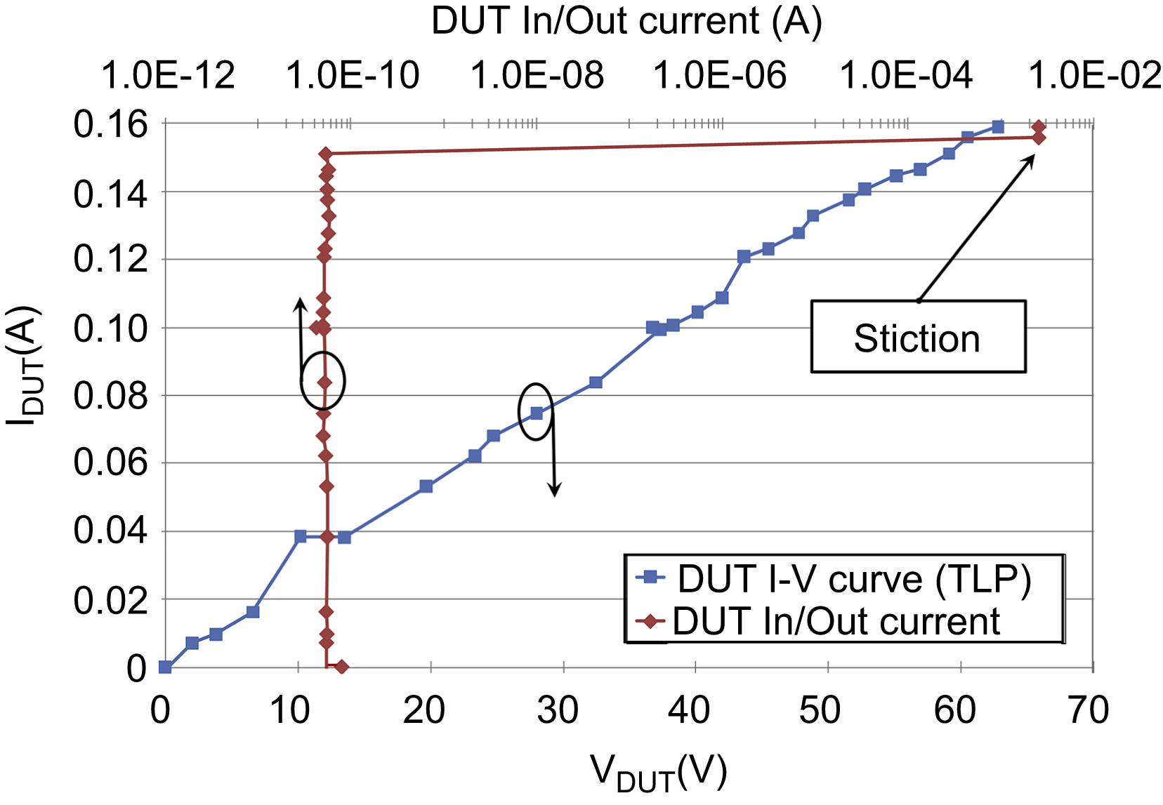
Figure 18.20 Result of the transmission line pulse (TLP) technique applied to the MEMS switch in Fig. 18.19. The increasing intensity of the driven current pulse leads to stiction due to microwelding, when the bias voltage (VDUT) driving the pulsing is around 60 V. DUT, device under test.

Figure 18.21 Vertical velocity of the microelectromechanical system contact areas versus time, when a pulsed current is driven through the microheater in Fig. 18.19(b). The release of the membrane after the tearing apart of microwelding joints, is visible around 28 s. RF-MEMS, radio frequency microelectromechanical system.

Figure 18.22 Microscope image of the microelectromechanical system (MEMS) contact areas after the activation of the microheater. The black spots indicate where microwelding joints were located. The MEMS membrane was moved apart to make visible the underlying contacts.
Further additional solution employing active restoring mechanism is the one using a push/pull design for the MEMS membrane. In the work reported in Solazzi et al. (2010), a design called toggle-type switch employs a pair of biasing electrodes that, when driven, allow to apply an upward force to the central electrode, i.e., where stiction may occur. Such an active force corroborates the mechanical restoring one, helping recover from malfunctioning.
For all kinds of MEMS/RF-MEMS, packaging is also a crucial issue (Wilkerson et al., 2001; Tilmans et al., 2003; Seki, 2004) because it impacts the insertion losses and also the reliability since hermetic packaging may ensure dry air environment to the MEMS. The field of packaging for RF-MEMS was investigated for a long time, and different solutions have been developed for the so-called 0-level packaging, i.e., the encapsulation of RF-MEMS at single component level. Two of the most common technology solutions for the realization of a protective cap are going to be briefly discussed.
In the first one, named WLP, an entire additional wafer is exploited to fabricate the package and is then aligned and bonded to the RF-MEMS device wafer, as reported in Iannacci (2013a). In this case, a rather diffused solution to redistribute the electrical signals from the intrinsic RF-MEMS device to the outside world is by means of vertical through-wafer vias across the package wafer, then filled with conductive material, as widely discussed in Iannacci et al. (2008a), Sekhar et al. (2012), Chen et al. (2013), Vitale et al. (2015), Tian et al. (2006).
A different solution at technology level consists in realizing a protective cap above each RF-MEMS device, without relying on an additional wafer to be aligned and bonded (like in WLP), but rather in performing additional (back end) fabrication steps, as soon as the RF-MEMS process is complete, aimed to manufacture a packaging lid just above the intrinsic functional device, while maintaining access to the electrical interconnects and RF terminations, as reported in Gillot et al. (2005), Wunnicke et al. (2011), Zekry et al. (2011) and Persano et al. (2016).
In any case, regardless of the specific technology solution for the realization of the cap, packaging and encapsulation of RF-MEMS pose additional issues if compared with other devices. As a matter of fact, the applied package, as well as the strategy selected for the redistribution of electrical signals, influences the RF characteristics of the initial (naked) devices, thus jeopardizing the outstanding performance of such passives. In light of these considerations, it is rather important to account for the influence of the package already during the RF-MEMS design phase, as discussed in Jourdain et al. (2003b), Iannacci and Bartek (2006), Kim et al. (2007), Jandhyala et al. (2009).
18.9. RF-MEMS power capability
As previously pointed out, the reliability of RF-MEMS needs to be studied with devices under environmental and operation conditions comparable to the final application, e.g., concerning the temperature, presence of gases, activation cycling, and RF power. This section reports the power behavior of RF-MEMS switches. We present investigations on the failure mechanism of RF-MEMS switches under high RF power condition (Grenier et al., 2005; Pillans et al., 2002; Muldavin et al., 2003; Lu et al., 2005b).
To illustrate the degradation mechanism, which appears under presence of RF power, two sets of experiments were performed on the device, as depicted in Fig. 18.23.
For the first set of experiments, the extracted upstate (Cup) and downstate (Cdown) capacitance of the RF-MEMS device after RF power stresses was monitored. Before any stress was applied, the values of Cup and Cdown were extracted and they correspond to 65 fF and 0.84 pF, respectively. Fig. 18.23 summarizes the experimental data with RF power stress up to 6.3 W, i.e., the maximum power delivered by the setup. We report a 50 fF upstate capacitor rise corresponding to only 0.12 dB insertion loss degradation at 10 GHz, which is negligible and proves that no self-actuation or microwave degradation occurs up to 6.3 W. Fig. 18.23 also demonstrates no significant degradation of the downstate capacitance. On the contrary, an improvement of 12% is obtained, which translates into an isolation improvement of only 0.8 dB.
A deeper insight of the switch power behavior is found with the second set of experiments. The rising RF power stress from 0 to 6.3 W, when the bridge is in the downstate, was induced and the electromechanical evolution of the RF-MEMS was monitored (we have already demonstrated that no degradation of microwave performance appears). Fig. 18.24 presents the measurements of the microwave transmission (S21 parameter) of the RF-MEMS (typically, at 10 GHz) for DC actuation voltage ranging from 0 to 40 V and down to 0 V. From this measurement, the behavior versus the RF power stress for what concerns the insertion loss of the MEMS switch (S21 for 0 VDC), the isolation (S21 for 40 VDC), and the pull-in/pull-out voltages can be monitored.
The observed behavior is associated with the fact that, up to 3 W, no degradation of the device may be noted. Degradation occurs between 3 and 3.8 W. For power stress greater than 4 W, a magnification of the degradation mechanism reflected by a different electromechanical behavior is shown. The degradation mechanism signature corresponds to a decrease of the pull-in voltage, which is related to a modification of the overall stiffness. The combination of these experiments and the observed results suggest that a mechanical degradation of the movable membrane occurs at high RF power, as a consequence of high-current density above the electromigration threshold.
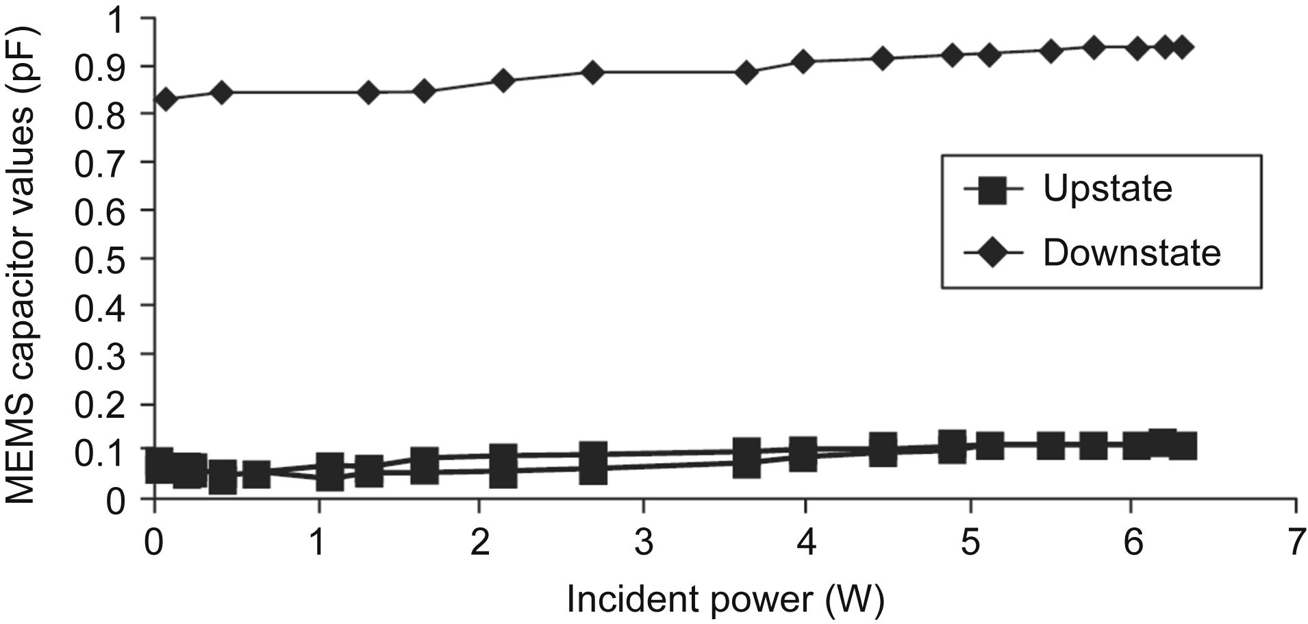
Figure 18.23 Measured capacitor values (up and down) versus radio frequency power stress intensity. MEMS, microelectromechanical system.

Figure 18.24 Microwave behavior at 10 GHz versus DC control voltage for different power stress levels. MEMS, microelectromechanical system.
To understand the effects of such failure on the electromechanical behavior, electromagnetic simulations with SONNET software permit the prediction of the RF current density at 10 GHz. For 3 and 3.8 W of injected power, current densities of 112 and 124 GA/m2 for the bridge upstate and downstate were simulated, respectively. These results are very close to the electromigration threshold values reported in the literature for gold metallization (around 140 GA/m2 at 80°C). This agreement between extracted failure current density and the electromigration threshold, strongly suggests that the main failure phenomenon occurs in the movable part of the RF-MEMS and translates into degradation of electromechanical performance.
Rather robust RF-MEMS switches have been realized also in other technologies. In particular, some of them were demonstrated to stand RF power as high as 5.6 W, notably, in hot switching conditions, i.e., pulled-in and released while the RF signal is traveling across the device. Such RF-MEMS switches are reported and discussed in more details in Palego et al. (2010) and Solazzi et al. (2012).
18.10. Cointegration of RF-MEMS-based circuits with integrated circuits
One key issue of RF-MEMS technology is the compatibility with CMOS fabrication platforms. Such a feature opens the door to the cointegration of passive and active functions with RF-MEMS, which are the key to bring high-level performances, in terms of tunability or reconfigurability, to the systems. One critical element of cointegration consists in the tolerable thermal budget. As far as CMOS technology is concerned, this limit is traditionally considered to be around 400°C. Above this temperature, the circuits begin to degrade (Grenier et al., 2004).

Figure 18.25 Placement of radio frequency microelectromechanical system (RF-MEMS) with integrated circuit (IC). (a) RF-MEMS above-IC and (b) RF-MEMS within-IC. CMOS, complementary metal–oxide semiconductor.
The second key factor in the integration of RF-MEMS passive components with ICs is related to cost. IC substrates are particularly expensive because of the demanding process steps and photolithographic masks required for the realization of transistors and integrated passive components. As far as the monolithic integration of RF-MEMS is concerned, it is traditionally realized through postprocessing steps, after the realization of the ICs, as indicated in Fig. 18.25(a). For example, Nguyen (2008) demonstrated vibrating disk mechanical resonators realized on a CMOS substrate, meant for integrated micromechanical RFFEs.
More recently, the new opportunities offered by thick dielectric and metallic layers within IC technologies have opened new horizons for integration of MEMS and ICs (Fedder et al., 2008), as indicated in Fig. 18.25(b). An excellent tuning ratio of digital capacitors of up to 60:1 has been demonstrated with the employment of the top dielectric and metallic layers available for ICs (Reinke et al., 2011).
Looking into materials different from silicon, RF-MEMS SPDT integrated on a gallium arsenide (GaAs) platform together with an LNA enables up to 1 dB noise figure improvement for K-band operation (Malmqvist et al., 2012), with final monolithic microwave integrated circuit surface of only 3 mm2. Ulusoy et al. (2012) demonstrated a similar benefit on a BiCMOS platform. A 60–77 GHz switchable LNA integrated with RF-MEMS switches has been realized with a 0.25 μm silicon germanium and carbon (SiGe-C) BiCMOS technology. Even if the two RF-MEMS devices occupy a large surface compared with the LNA core, the circuit covers a surface of only 0.8 mm2.
The dual approach that differentiates from monolithic manufacturing of RF-MEMS and active (e.g., CMOS) technologies is the hybridization of different components through their integration. In this case, it is easy to understand that the 0-level package, meant in the first place to protect the RF-MEMS device, plays a crucial role in facilitating its integration and interfacing to active components, as well. The package, indeed, in redistributing electrical signals from the device level to the external world is a key element to interface the RF-MEMS component to the system or subsystem into which it is meant to be employed. Moreover, in some cases, the package itself can provide housing to integrated electronics, by means of recesses and small sockets obtained in the substrate used for the protective lid (Iannacci, 2013a). The latter option is of particular interest for RF-MEMS, which in any case require active electronics to be driven and operated.
Apart from System in Package solutions, a wide portfolio of options is available to achieve effective and low-cost integration of MEMS and RF-MEMS devices to the rest of the systems, them being commonly indicated as SMTs. Among them, the most commonly used are wire bonding and flip chip (Jin et al., 2010; Lau et al., 2010; Fischer et al., 2015; Chiao et al., 2012).
In this context, RF-MEMS die varactors were cointegrated (using the flip-chip method) on a laminate board with a bipolar junction and CMOS transistor (BiCMOS) class-F PA. This provides up to 10% improvement in efficiency for a dual-band 0.9/1.8 GHz operation (De Graauw et al., 2006). Another example, in which an RF-MEMS-based reconfigurable impedance matching tuner has been wire bonded to a class-E CMOS PA, was already discussed before and reported in Larcher et al. (2009).
In conclusion, both monolithic fabrication and integration of heterogeneous technologies are viable and pursuable solutions. Of course, trade-offs exist, and they must be carefully evaluated. Monolithic solutions are typically more expensive and represent a sensible option when specific very high performances must be achieved. On the other hand, integration of different components through SMTs ensures high performances as well, are typically low cost and, therefore, represent the best option in most practical cases.
18.11. Conclusions
RF-MEMS technology was introduced since the turn of the millennium, to develop smart RF systems exhibiting a high level of integration and new functionalities, such as reconfigurability (the ability to switch between different standards) or to self-repair, as well as high-level electrical performance up to millimeter wave frequencies.
Despite numerous open issues were unavoidably deployed along the maturation path of RF-MEMS, the effort invested by the research and industrial communities, made possible, across the last 10–15 years, to reach technology readiness fully compatible with commercial applications. Among the aforementioned obstacles, reliability, power handling, as well as packaging and integration of RF passives realized in microsystem technology are the most relevant ones.
From a different perspective, there have always been significant expectations around the successful exploitation of RF-MEMS components within large commercial applications, such as mobile handsets, short-range radar systems, and, more in general, RF transmitters/receivers (transceivers). Most part of those flattering forecasts were systematically disappointed. One of the driving reasons for this (sort of) failure was the set of additional problems linked to RF-MEMS technology mentioned above, i.e., substantially, reliability, packaging, and integration. However, this is just a part of the whole picture.
The underlying motivation for the missed breakthrough of RF-MEMS in the past decade should be sought elsewhere. Already in the early days of RF-MEMS, i.e., at the turn of the millennium, the approach to envisioning their commercial exploitation was too much technology-push driven. Back then, it was like if entire architectures of RF transceivers should had been reengineered to accommodate RF-MEMS devices. This was most probably ignited by the remarkable performance that can be nimbly achieved by means of such a technology.
Nonetheless, from the point of view of the market, there were not consistent demands pushing toward a technology solution that was not yet mature, and that was leading to additional costs and effort to be employed. All in all, just to mention an example, the first generations of mobile handsets (i.e., 2G and 3G) worked rather well even without RF-MEMS.
In more recent times, the scenario commenced to show some significant changes. 4G-LTE smartphones started to exhibit the need for adaptive impedance tuning between the antenna and the RFFE. As a result, impedance tuners started to be the first successful commercial exploitation of RF-MEMS technology. In other words, as soon as the approach started to be more market-pull rather than technology-push driven, RF-MEMS technology was recognized as the best candidate to meet the emerging requirements.
In light of this modified landscape, the upcoming 5G communication standards seem to be the field in which most part of the RF-MEMS value could be extracted.
In this chapter, a broad overview on RF-MEMS technology was provided, sketching nearly 15 years of significant achievements reached by the research community and providing an outlook on future exploitation of such a promising solution.
..................Content has been hidden....................
You can't read the all page of ebook, please click here login for view all page.