Smart temperature sensors and temperature sensor systems
Gerard C.M. Meijer1,4, Guijie Wang1,3, and Ali Heidary1,2,31Delft University of Technology, Delft, The Netherlands2Guilan University, Rasht, Iran3Smartec, Breda, The Netherlands4SensArt, Delft, The Netherlands
Abstract
For temperature sensing in smart sensors and microelectromechanical systems (MEMS), the most commonly used elements are transistors, thermocouples, and thermopiles because these elements can be implemented with integrated circuit (IC) technology. At the system level, also other sensor elements are used. A comparison between different types of sensing elements is presented.
For the temperature range of −55 to 150°C, bipolar junction transistors are very suited to be applied as temperature sensors because they can be fabricated in almost any standard IC technology, together with other circuitry. With similar circuits, bandgap voltage references can be made, which enables doing ratiometric measurements, where temperature-sensitive voltages are compared with an intrinsic reference voltage.
In complementary metal-oxide semiconductor (CMOS) technology, component matching is poor. Yet, when using CMOS analog circuits, a very high precision can be achieved by using error-reduction techniques, such as dynamic element matching and chopping. These methods have been applied in a smart temperature sensor with a duty cycle modulated output signal, which is presented as case study. Even with a very low energy consumption, a high precision is achieved.
Keywords
Chopping; CMOS temperature sensor; Duty cycle modulation; Dynamic element matching (DEM); Integrated temperature sensors; Smart temperature sensors; Temperature sensor systems
3.1. Introduction
In addition to sensor elements, smart sensors are equipped with built-in electronics so that they can interact with other devices to process the data received (see Chapter 1; Taymanov and Sapozhnikova, 2017). For such sensors the technologies for producing and using the sensors and the electronic components should be compatible. This compatibility should be required not only in the production phase but also for circumstances that occur during the lifetime of the application.
This requirement conflict is clearly evident: On the one hand, sensor elements should interact with the physical environment as smoothly as possible, whereas on the other hand the electronic circuitry should be protected from hostile environments to protect it from mechanical damage and corrosion. Yet for some sensors this problem hardly exists. For instance, in smart temperature sensors and in accelerometers it is possible to assemble the sensor chips in hermetically closed packages, whereas the physical quantities, being temperature and acceleration, can still be measured because with proper care the values of the mentioned quantities are equal inside and outside of the package.
The maximum temperature range of smart temperature sensors is limited to that of the electronic circuitry. Usually, this is in the range of about −50°C to +140°C. Yet, when using nonconventional sensing elements, such as thermal delay lines, it is possible to fabricate smart sensors for a much wider range (Makinwa, 2010). Moreover, even in conventional integrated-circuit (IC) technology some electronic circuits can also function at high temperatures, even up to 300°C (Jong de and Meijer, 1998). For higher temperatures, other types of sensors have to be used. For instance, for temperature sensors, platinum (Pt) resistors can be used for the temperature range of about −260°C to +1000°C, whereas with a variety of thermocouples an even wider range from about −270°C to +3500°C can be covered.
It should be noted that thermocouples do not measure absolute temperature but only the temperature difference between the reference junction and the measurement junction. What can be used to measure the temperature of the reference junction is a smart temperature sensor, such as the ones dealt with in this chapter. In fact, a smart temperature sensor can also be integrated together with a voltage reference and an interface circuit to process the output voltage of the thermocouple and to make a suitable output for a microcontroller (Khadouri et al., 1997).
There are many other examples of sensor systems in which physical/chemical signals have to be measured in combination with temperature and where integration with one or more smart temperature sensors could be a good option. For instance, in thermal infrared (IR) sensors, the radiation emitted from an object is converted into temperature differences in a heat absorber. The absorbed heat is related in a nonlinear way to the temperatures of both the object and the absorber (Herwaarden van, 2008). The temperature of the absorber will rise with respect to that of the bulk of the detector, creating a temperature difference, which is measured with a thermopile. With the thermopile voltage and the temperature of the detector bulk as input signals for an interface circuit, the IR radiation can easily be calculated.
This chapter is mainly limited to the concepts, design, and application of smart temperature sensors fabricated in complementary metal-oxide semiconductor (CMOS) technology. Attention is focused on properties such as accuracy, resolution, and optimization of energy consumption. It will be shown how users can apply their knowledge to optimize temperature sensor systems for accuracy, speed, and maintenance in industrial applications. For a broad overview regarding temperature measurements and topics outside the scope of this chapter the reader is referred to, for instance, Michalski et al. (2001).
3.2. Measuring temperature, temperature differences, and temperature changes in industrial applications
Temperature sensors with a high level of accuracy are expensive, which is mainly due to the required calibration and trimming procedures. Moreover, the accuracy should regularly be checked and care should be taken during application, for instance, during thermal cycling or a heavy mechanical load, that the required accuracy is still maintained.
In many industrial applications, stability and good resolution over a certain time interval are more important than accuracy with respect to standards.
Example 1. Monitoring temperature changes over time. Suppose that temperature sensors are used to monitor the thermal effects of biomedical or physical activities, as performed for characterizing materials and or monitoring chemical and physical processes. In such cases, the temperature changes over time have to be followed over a certain time interval with sufficient resolution. The absolute temperature is less significant and sometimes only monitored to compensate for the effects of certain temperature coefficients. Therefore, for such applications, the main requirements for the temperature sensors might concern resolution and stability, whereas the absolute accuracy might be of less importance. On one hand, sensors with resolution and stability better than 1mK can easily be found, whereas on the other hand sensors with an accuracy of 1mK are very expensive. Moreover, it is difficult to maintain such high accuracy for a long period.
Example 2. Monitoring temperature differences. The intensity of IR radiation can be measured with a thermal sensor. In such a sensor, radiation is converted into heat at a heat-absorbing membrane. Via a well-characterized thermal conductor this heat flows into the bulk of the sensor. The temperature difference between both ends of the thermal conductor is a measure for the absorbed heat. Seebeck sensors are very well suited to measure temperature differences because of a feature that allows temperature differences to be measured offset-free. With some nonlinearity, the output voltage of these sensors is proportional to the temperature difference between the two junctions (Herwaarden van, 2008). In such an application, it makes sense to measure also the temperature of one of the junctions, for instance, to compensate for the effects of the temperature dependency of heat conductance and the Seebeck coefficient. Usually, the accuracy required for the temperature sensor is much lower than for that of the temperature-difference sensor.
3.3. Temperature-sensing elements
3.3.1. Introduction
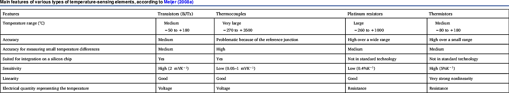
In smart temperature sensor systems and microelectromechanical systems (MEMS), often integrated sensors are used, which combine sensing elements with the interface electronics needed to communicate with, for instance, microcontrollers. In addition to integrated sensors, in such systems also discrete sensing elements can be applied. Discrete elements are used, for instance, for calibration and testing. Discrete elements are also used in environments in which the temperatures are beyond the range of what interface electronics can tolerate. Table 3.1 (Meijer, 2008a) summarizes the main features of some commonly used on-chip and discrete sensing elements for temperature sensor systems and MEMS.
Bipolar junction transistors (BJTs) and thermistors belong to the most sensitive devices in this table. Often BJTs are used with short-circuited collector-base connection1 and are biased with a well-controlled current. This way of biasing has the advantage that the resulting base-emitter voltage is almost linearly related to the temperature (Meijer, 2008a). Also the thermistor characteristics can be linearized by applying series or shunt resistors, at the cost of reducing the sensitivity (Meijer, 2008a). A high sensitivity can be useful because it will relax the accuracy requirements of processing circuits. Actually, any equivalent input error of the processing circuits will be divided by the sensor sensitivity when calculating the corresponding temperature error. Often it is not so difficult to design a good processing circuit. In that case, the accuracy of sensor elements is more important than their sensitivity.
For a major part, the inaccuracy of temperature-sensing elements is caused by the cross effects of mechanical stress and therefore also by changes in the mechanical stress during, for instance, thermal cycling or aging. For the same reasons, the sensor accuracy is affected by mechanical stress remaining after fabrication and packaging of the sensor elements. When comparing transistor and thermistor properties, at the important temperature range around 300K, thermistors have a better accuracy. That is the reason that thermistors are often applied in sensor systems. On the other hand, transistors belong to the main components in ICs. Therefore, transistors can be fabricated as on-chip temperature sensor component. Consequently, innovations in BJT-based temperature sensors have followed the rapid development and innovation in IC technology. For this reason, in Smart Sensors and MEMS, BJTs are the favorite temperature-sensing elements. Therefore, this chapter will mainly be devoted to BJT-based temperature sensors and corresponding temperature sensor systems.
Table 3.1
Main features of various types of temperature-sensing elements, according to Meijer (2008a)
Features
Transistors (BJTs)
Thermocouples
Platinum resistors
Thermistors
Temperature range (°C)
Medium
−50 to +180
Very large
−270 to +3500
Large
−260 to +1000
Medium
−80 to +180
Accuracy
Medium
Problematic because of the reference junction
High over a wide range
High over a small range
Accuracy for measuring small temperature differences
Medium
High
Medium
Medium
Suited for integration on a silicon chip
Yes
Yes
Not in standard technology
Not in standard technology
Sensitivity
High (2mVK−1)
Low (0.05–1mVK−1)
Low (0.4%K−1)
High (5%K−1)
Linearity
Good
Good
Good
Very strong nonlinearity
Electrical quantity representing the temperature
Voltage
Voltage
Resistance
Resistance
Thermocouples generate a voltage that is proportional to a temperature difference between, for instance, a reference junction and a measurement junction.
Thermopiles consist of a number of serial-connected thermocouples and are also used to measure temperature differences. Thermopiles can be fabricated with IC technology and are very suited for application in thermal sensors. In thermal sensors, physical quantities are measured by transducing the physical signals into temperature differences first, and then transducing this temperature difference into a thermopile voltage. Usually, in such sensors a reference temperature is also measured, for instance, with a bipolar transistor or a temperature-sensitive resistor. IR sensors, including the popular clinical ear thermometers, are examples of thermal sensors, in which radiation is absorbed at a cantilever beam (Herwaarden van, 2008), which causes a temperature difference that is measured with a thermopile. Measuring absolute temperature with a thermocouple or an IR sensor also requires the use of an absolute temperature sensor, for instance, a thermistor or a transistor, to measure a reference temperature.
In industrial systems, often discrete temperature-sensing elements are used,because of their high accuracy and excellent long-term stability. The most commonly used elements are Pt resistors, thermocouples, and thermistors. Because of their stability, platinum resistors are listed in the 1990 International Temperature Scale as interpolating temperature standard in the −259.4°C to 961.9°C temperature range (Michalski et al., 2001). For higher temperatures, other types of sensors, such as certain types of thermocouples, are used. Because of their low cost and high reliability, discrete thermocouples are widely used in industrial applications, where different types are available for different temperature ranges.
Thermistors are very sensitive but not as stable as Pt resistors. They are widely applied for the temperature range of about −80°C to 180°C. In addition to their high sensitivity, thermistors offer the advantages of being small in size and inexpensive. However, their strong nonlinearity complicates the processing of the thermistor signal. Linearization can be obtained with shunt and series resistors (Meijer, 2008a), at the cost of reduced sensitivity. Some sensor interfaces, such as the universal sensor interface of Smartec (2016a), offer special processing modes for thermistors, including linearization.
Over the last decades, innovations in temperature sensor systems implemented with discrete temperature-sensing elements mainly concerned the development of electronic interfaces (Smartec, 2016a; Meijer, 2008b; Khadouri et al., 1997). For more details related to discrete temperature-sensing elements and the corresponding measurement systems, the reader is referred to specialized literature (Michalski et al., 2001).
3.3.2. Temperature sensor characteristics of bipolar junction transistors
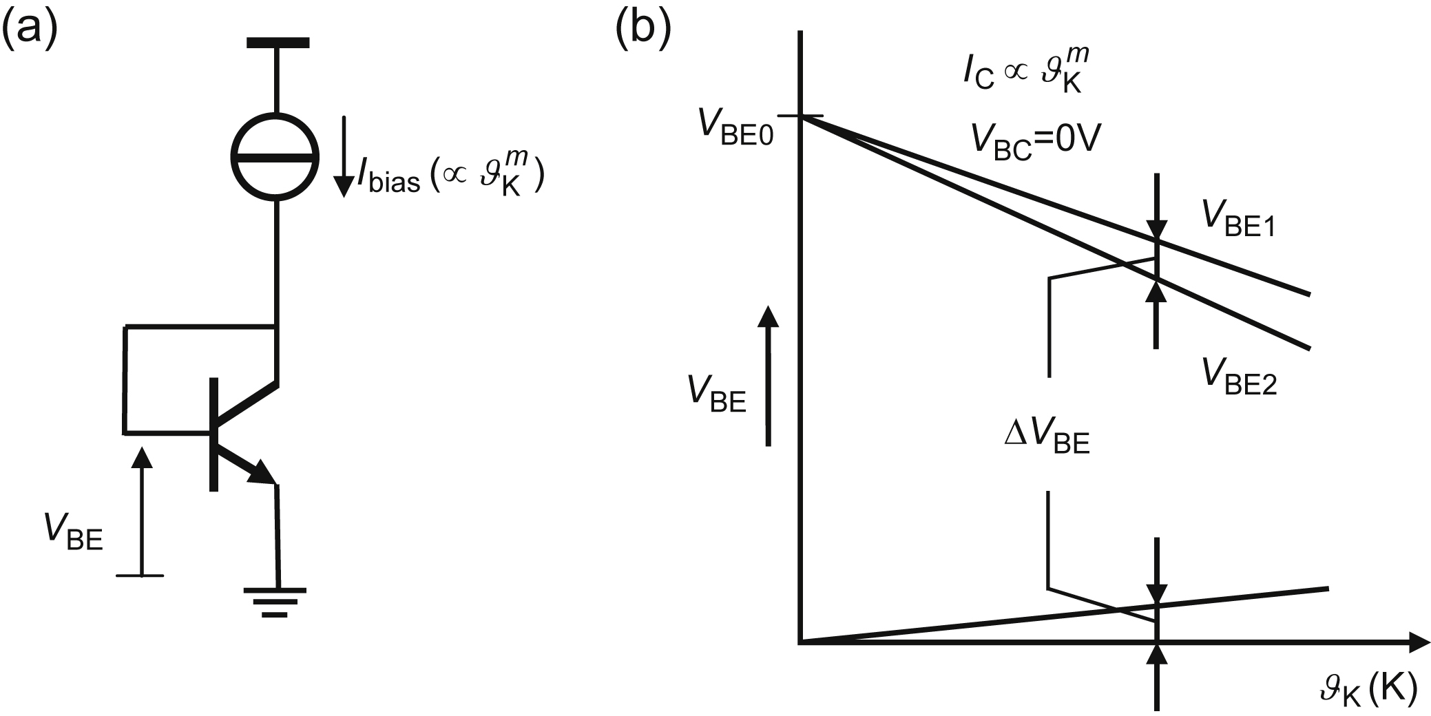
Transistors are suited to be applied for a limited temperature range of about (−55°C to 150°C). Their main advantages are that they are suited to be integrated in standard IC technology, their high sensitivity, and acceptable long-term stability. Fig. 3.1(a) shows the simplest way to bias a temperature-sensing transistor: The collector and base are short-circuited, and a bias current Ibias is supplied. Usually, the base current is much smaller than the collector current IC, so that it holds that IC≈Ibias. The favorable properties of transistors for temperature sensor applications are due to the predictable and accurate way in which the base-emitter voltage VBE is related to the temperature. Fig. 3.1(b), plots the base-emitter voltages versus the temperature for two identical transistors, which are biased at different collector current densities. There are two methods for determining the temperature from VBE: as shown in
Figure 3.1 (a) Bipolar junction transistor (BJT) with short-circuited collector and base operated at a constant current Ibias; (b) The base-emitter voltage VBE decreases almost linearly with temperature ϑK, whereas the difference (ΔVBE) between two BJTs biased with different current densities increases linearly with the absolute temperature ϑK.
1. In the first method, VBE of a single transistor is the measure for temperature. This voltage has a negative temperature coefficient (Fig. 3.1(b)).
2. In the second method, the measure for temperature is the difference (ΔVBE) between the base-emitter voltages of two transistors biased at different current densities (not shown in Fig. 3.1(a)). This voltage is proportional to absolute temperature (PTAT). Thus, this voltage has a positive temperature coefficient (Fig. 3.1(b)).
Any desired linear temperature characteristic can be realized by amplifying and/or adding the voltages mentioned in (1) and (2). As will be shown in this chapter, this property is widely applied in smart temperature sensors. This favorable transistor behavior will now be explored in more detail.
Let us assume that the collector-base voltage of the sensor transistor is constant. This is desirable because, due to the so-called Early effect, changes in the collector-base voltage affect the base width (base-width modulation) and therefore the base-emitter voltage. Most easy is to make the collector-base voltage equal to 0V, by short-circuiting (Fig. 3.1(a)). For the IC(VBE) characteristic of an NPN transistor it holds by good approximation (Meijer, 2008a) that:
IC=AeJsexpqVBEkϑK,
(3.1)
where IC is the collector current, Ae is the emitter area, Js is the saturation current density, which highly depends on the temperature, q is the electron charge, ϑK is the absolute temperature2, and k is Boltzmann's constant (k/q=86.17μV/K). For PNP transistors a similar equation is valid but with opposite signs for the currents and voltages.
The temperature sensor transistor has to be biased at a (collector) current with a well-established temperature dependence. Because it is quite easy to create a current that is proportional to some power m of ϑK, we suppose that
IC∝ϑmK.
(3.2)
The saturation current density Js strongly depends on the temperature (Slotboom and de Graaf, 1976). Taking this into account it can be shown that (Meijer, 1982):
VBE(ϑK)=VBE0+λϑK+(η−m)kϑKq(ϑK−ϑK,rϑK−lnϑKϑK,r),
(3.3)
where
VBE0=Vg0+(η−m)kϑK,rq,
(3.4)
where Vg0 is the linearly extrapolated bandgap voltage at 0 K and η is a constant, which slightly depends on the doping level. Furthermore, VBE0 is the extrapolated value of the tangent to the VBE(ϑK) curve for an arbitrary reference temperature ϑK,r, and λ represents the slope of that tangent. Typical empirical values for the parameters Vg0 and η are 1160mV and 4, respectively. The nonlinearity in VBE(ϑK) is represented by the last term in Eq. (3.3). For η−m=3, the maximum nonlinearity over the −55°C to 150°C temperature range corresponds to about 20°C (Meijer, 2008a). Usually, in smart temperature sensors this nonlinearity is compensated with on-chip circuity.
To obtain an impression of the linear terms of Eq. (3.3), let us substitute Vg0=1160mV, η=4, and, for example, m=1 (IC is PTAT), ϑK,r=323K (in the middle of the range). When VBE(ϑK,r)=547mV (this value depends on the biasing current density and the applied technology), then we find for the extrapolated VBE value at 0 K, that VBE0=1243.5mV and for the PTAT term λϑK in (3.3) that λ=−2.156mV/K.
3.3.3. ΔVBE temperature sensors
In most of today's temperature sensors both voltages VBE and the difference ΔVBE between the base-emitter voltages of two transistors are used as a measure for temperature (see Fig. 3.2). When comparing these two voltages, the following features are found:
Figure 3.2 (a) Principle of a circuit to generate the difference ΔVBE between the base-emitter voltages of two transistors Q1 and Q2 (Meijer, 2008a), (b) Simple proportional to absolute temperature current source.
• Voltage ΔVBE is immune to variations in doping concentration and therefore its tolerances are smaller than those of voltage VBE. For this reason, the latter one is often calibrated and trimmed.
• Voltage ΔVBE is much smaller than VBE and therefore more sensitive to noise and interference.
The reason to use both voltages is that they have opposite temperature coefficients. Thus, an amplified voltage AΔVBE can be used to compensate the temperature coefficient of VBE, which results in a temperature-independent voltage (the so-called bandgap-reference voltage). This voltage can be used as an internal (intrinsic) reference, which is an important feature to enable ratiometric signal processing, as will be discussed in Section 3.6.
Fig. 3.2(a) shows a simple circuit that generates the voltage ΔVBE. For accuracy reasons, it is important that all of the transistors have the same temperature ϑK. Because silicon is a good thermal conductor, this can easily be achieved when the circuit is fabricated as an IC. Transistors Q3 and Q2 are implemented with a number p and r of transistors in parallel. A group of parallel-connected transistors functions equivalent to a multiemitter transistor, with the same number of emitters in parallel. When applying Eq. (3.1) for the group of r parallel-connected transistors Q2 and the single transistor Q1, we substitute for emitter areas that Ae2=rAe and Ae1=Ae, respectively. The value of Js does not depend on the area. Therefore, for the single transistor Q1 and the transistor group Q2 it holds that Js2=Js1.
Because all transistors are operated at the same temperature ϑK, applying Eq. (3.1) yields
Transistors Q4, Q3, and Q5 (Fig. 3.2(a)) are operated in a so-called current-mirror configuration. Because of the interconnected base-emitter terminals and the equal temperature ϑK, the collector-current densities of these three transistors are equal. Because transistor Q3 is implemented with p components in parallel, the collector current ratio IC3/IC4=IC1/IC2 is kept at a constant accurate value p, which does not depend on temperature or other physical parameters. Taking into account this feature and when ignoring the effects of the (small) base currents, Eq. (3.5) can be rewritten as
ΔVBE=kϑKqln(pr).
(3.6)
This voltage is PTAT. Using this feature, a so-called PTAT current source can be built. Fig. 3.2(b) shows a simple PTAT current source, in which a PTAT voltage ΔVBE according to Eq. (3.6) is generated over resistor R2. As a result through this resistor a current ΔVBE/R2 will flow, which is also the biasing current of transistors Q2 and Q4 and will be amplified by current mirror Q4 and Q3 with a factor r=3. So, the circuit is self-biasing. In practical circuits, a very small start-up current is inserted. Soon after this start-up, all currents and voltages will converge to their final stationary values. When a high accuracy is required, in practical circuits also measures are taken to reduce the effects of the base currents, such as base-current compensation, and changes of the supply voltage, such as cascoding.
3.3.4. Bipolar junction transistors in complementary metal-oxide semiconductor (CMOS) technology
The fabrication of BJT-based temperature sensors is not limited to bipolar technology. In the next sections it will be shown that fabrication of such sensors in CMOS technology can result in excellent sensors, which can be fabricated at lower costs. In addition, substrate PNP (bipolar) transistors, which can easily be fabricated in CMOS technology, are shown to be less sensitive to mechanical stress than NPN transistors fabricated in other technologies (Fruett and Meijer, 2002). This explains why the CMOS temperature sensors discussed in the next sections show less packaging shift and have a better long-term stability than earlier bipolar designs.
3.4. Basic concepts of smart temperature sensors
3.4.1. Architectures of smart temperature sensor systems
In smart temperature sensors, the sensing elements and sensor-interface electronics are combined in a single chip. This combination can be very favorable in terms of standardization of the output signal, accuracy, reliability, possibility of overall calibration, etc. Such temperature sensors can function in the important intermediate temperature range of −50°C to +180°C, with high accuracy and high reliability. The sensor chips can be delivered in a wide variety of packages. Using a metal encapsulation offers the advantage of hermetical sealing, which is good for the long-term stability. Moreover, because of the high thermal conductivity of the encapsulation, there can still be a good thermal interaction between the chip and its thermal environment.
Figure 3.3 Possible system setup with a microcontroller, some smart temperature sensors and discrete temperature-sensing elements with separated sensor interfaces.
Sometimes, for temperature sensors it is undesirable to combine electronics and sensing elements. For instance, when a very wide temperature range is required, or when there are extreme requirements for stability or packaging. In such a case a smart sensor system could be designed, which consists of a discrete sensing element, a sensor interface, and a microcontroller as depicted in the right-hand side of Fig. 3.3(b).
It is also possible to fabricate microcontrollers and smart sensors or sensor-interface circuits on a single chip. However, the following considerations should be made
1. Microcontrollers are components produced in much higher volumes than those of smart sensors or sensor-interface circuits. Therefore it will cost less to produce microcontrollers and smart sensors or interface circuits separately.
2. Separated fabrication can also solve possible compatibility problems because microcontrollers are often produced in technologies, which are not suited for smart sensors.
3. To avoid self-heating, it is desired to reduce power dissipation in the sensor chip as much as possible. Therefore, within a temperature sensor system, it is often better to separate power-consuming signal-processing devices from the temperature-sensing devices.
Enabling communication between smart sensors and microcontrollers requires converting the analog signals into digital ones. For this purpose, an analog-to-digital converter (ADC) can be implemented either at the sensor chip or at the microcontroller chip. Many microcontrollers with built-in ADCs can be found on the market. As an alternative, a smart temperature sensor can also be implemented with output signals, which are microcontroller-compatible, for instance, a frequency-modulated signal, period-modulated signal, or duty-cycle-modulated (DCM) signal. In one of the very first smart temperature sensors on the market, a duty-cycle modulator was implemented in BICMOS technology. Recently, this sensor has been redesigned and implemented in low-cost CMOS technology (Smartec, 2016b). A strong feature of smart sensors with DCM output is that a (very) high resolution is obtained with rather low energy consumption.
When using CMOS technology, special circuit techniques are required to solve the problems posed by the large component mismatch and low-frequency noise. In the remaining part of this chapter details of these special techniques will be presented. As a case study, this is done for temperature sensors with a DCM output. It will be shown that a systematic application of the presented techniques will yield excellent circuit/system performance at low cost.
3.4.2. Temperature sensors with a duty-cycle-modulated (DEM) output
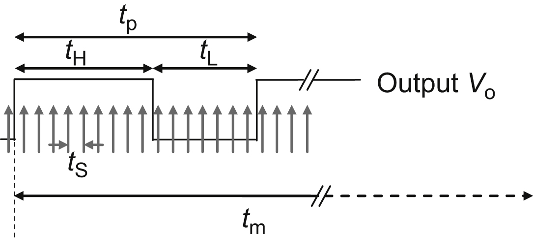
Smart sensors with a duty-cycle modulator produce a square-wave output voltage Vo (Fig. 3.4), where the duty cycle D equals the ratio of the high time tH and the period tp=tH+tL. Thus
D=tHtp.
(3.7)
An attractive feature of this output signal is that it can be interfaced both to the digital and the analog domains. Details about applications will be presented in Section 3.8.6, where it will be shown that such a sensor can also be applied without using a microcontroller or an ADC.
When a microcontroller is used to digitize the sensor output, the sensor output is connected to the timer input of the microcontroller, where the timer frequency is usually much higher than that of the sensor output. The numbers of sampling pulses during the HIGH time tH and the total period time tp are stored in two separate registers. In this way, the microcontroller performs the conversion from a time interval into digital numbers. To find the duty cycle D, the microcontroller performs a division according to Eq. (3.7). The sampling pulses are not synchronized with the output signal. Therefore, there will be some uncertainty about the exact moments that the time intervals tH and tp start and stop. This uncertainty is responsible for the occurrence of sampling noise, which is equivalent to the quantization noise of an ADC. Calculation shows that this sampling noise causes an error in the duty cycle with a standard deviation σD (Meijer, 2008a):
Figure 3.4 Duty-cycle-modulated output voltage Vo of a smart temperature sensor. The pulses show the sampling moments by a microcontroller timer, which indicates the cause of sampling noise.
σD=ts6tmtp√,
(3.8)
where tp is the period of the sensor signal, tm is the total measurement time, which equals Ntp (N is an integer number), and ts is the period of the sampling signal of the microcontroller.
Example 3.1: Suppose that the period of the sampling signal ts=20ns, the period of the output signal tp=0.3ms, the measurement time tm=30ms, so that N=100. Substitution of these values in Eq. (3.8) yields for the standard deviation in the duty cycle D that σD=2.72×10⁻⁶. For sensors with an extrapolated duty cycle changing from 0 to 1 for a temperature changing over 213°C (see Section 3.6), this sampling noise corresponds to a standard deviation in the temperature reading of about 0.58×10⁻³°C.
3.5. Methods to improve the accuracy of CMOS smart temperature-sensor systems
Mainly for economic reasons, CMOS technology has become the leading IC technology. However, for precision analog circuits, CMOS technology has two major drawbacks:
• Because of the large mismatch of CMOS components, basic circuits such as voltage dividers and current mirrors have large ratio errors, whereas operational amplifiers have a large offset voltage.
• CMOS transistors are surface devices. Therefore, the currents through CMOS transistors have a strong low-frequency (1/f) noise component.
Fortunately, there are methods to reduce the effects of these drawbacks. These methods are so successful, that nowadays, many CMOS precision circuits perform better than their bipolar counterparts. Two of these methods are Dynamic Element Matching (DEM), which reduces the effects of component mismatch, and Chopping, which reduces the effects of offset voltage and low-frequency noise. These methods will be briefly discussed in this section.
3.5.1. Dynamic element matching
A typical CMOS circuit, which generates PTAT voltage in CMOS technology is shown in Fig. 3.5(a), which depicts the CMOS version of the circuit in Fig. 3.2(a). The current mirror is implemented with CMOS transistors. As explained in Section 3.3.4, in CMOS technology it is also possible to fabricate (substrate) bipolar transistors. Such transistors are used to generate the voltages ΔVBE and VBE, which are applied in the smart temperature sensors, as discussed in Section 3.3. When the two PNP transistors are assumed to be equal, it holds that
Figure 3.5 Circuits generating proportional to absolute temperature voltages with CMOS technology: (a) Basic circuit resembling that in Fig. 3.2(a); (b) Similar circuit with dynamic element matching of the P-channel MOS (PMOS) transistors, according to Meijer (1995).
ΔVBE=kϑKqln(p)=kϑKqln3,
(3.9)
where p is the ratio of the summed drain currents of M1–M3 and the drain current of M4. However, mismatch between the PMOS transistors will cause an unpredictable error in the value of this ratio. By applying DEM, as shown in Fig. 3.5(b), the error induced by the mismatch between M1 and M4 can significantly be reduced, to the second order (Meijer, 1995). To apply DEM, the positions of transistors M1–M4 are sequentially interchanged, which is performed with switches Sp1 to Sp4. After one measurement cycle (four steps in this case), each of the transistors M1–M4 has been in the position of biasing Q1, whereas the others are biasing Q2. A complete cycle contains N (N=4) permutation steps. With each step the value of ΔVBE is stored. After a complete cycle, the average value of the four ΔVBE values approximates the nominal value of Eq. (3.9) very well. After A/D conversion of the ΔVBE values, the average value can be calculated in the microcontroller. As will be shown in the next sections, the same technique can be applied for other component pairs as well. It should be noted that the DEM technique reduces in a systematic way the errors caused by mismatch. Additionally, also the effects of low-frequency noise (with a frequency less than the cycling frequency of DEM) are also reduced in a systematic way. On the other hand, applying DEM has hardly any disadvantages: With a proper design, the effects of switch imperfections are negligible.
As will be shown in Section 3.7, for user of chips with DEM technique, it will be good to be informed about this, so that they can take full advantage of the benefits of this error-reduction technique (see Section 3.8.1).
3.5.2. Chopping
The basic idea of chopping in a sensor system is to modulate (chop) low-frequency sensor signals, so that a higher signal frequency is obtained, which can easily be distinguished from low-frequency nonidealities of amplifiers, such as offset and 1/f noise. At the amplifier output, the signal is chopped again (demodulated) so the frequency of the sensor signal returns to its original value, whereas offset and 1/f noise is converted into higher frequencies so that it can be removed with a low-pass filter. Today, many precision instrumentation amplifiers are equipped with built-in choppers (Huijsing, 2014). In sensor systems, choppers can also be applied in the physical domain, so that the advantages obtained with this technique affect a larger part of the signal processing chain.
It can be argued that the concepts of DEM and chopping show a large overlap: When chopping is applied by interchanging the input terminals of an amplifier, this is for a part similar to interchanging the two branches of the differential input amplifier, which is an act similar to DEM. In the rest of the chapter a case study is presented of a smart temperature sensor (Wang et al., 2017) in which both DEM and chopping are applied. It will be shown that those techniques can be merged very well and synchronized with respect to each other using the same clock signals.
3.6. Principles of BJT-based smart temperature sensors with DCM
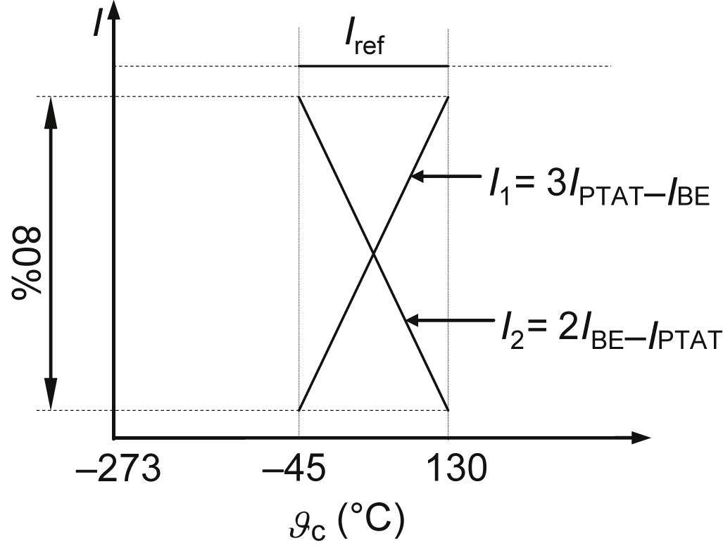
The case study presented here concerns a BJT-based smart temperature sensor with a DCM output. In this sensor, three temperature-sensing bipolar transistors are used to generate the basic voltages ΔVBE(ϑ) and VBE(ϑ). Voltage ΔVBE(ϑ) is generated as described in Section 3.3. The two basic voltages are converted into currents IPTAT=ΔVBE(ϑ)/RPTAT and IBE=VBE(ϑ)/RBE. Next, these currents are amplified, added, and subtracted. The final result of these operations is the generation of two currents I1 and I2, which have opposite temperature coefficients and are almost linearly related to temperature (Fig. 3.6).
Figure 3.6 Generated currents I1 and I2 and Iref=I1+I2 versus the temperature ϑC in degrees Celsius.
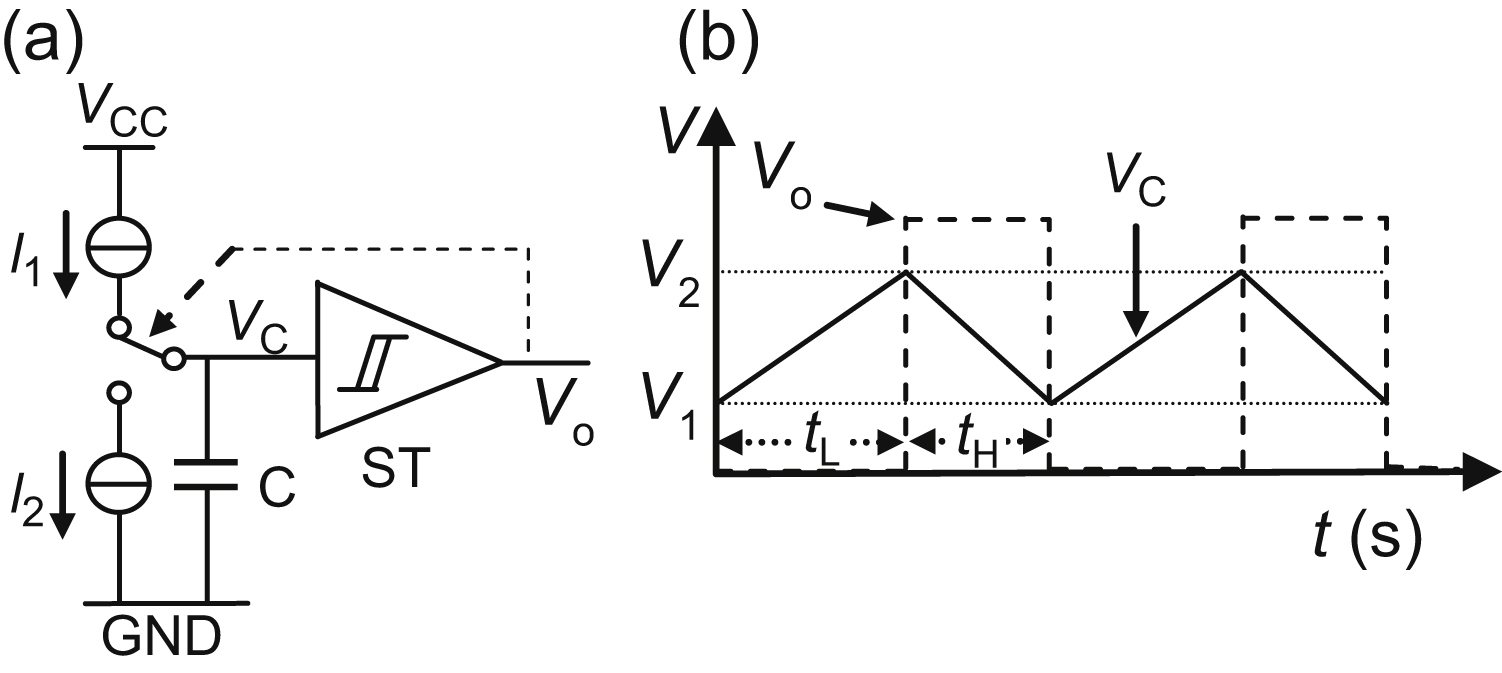
Figure 3.7 A smart sensor with a duty-cycle-modulated output signal: (a) Basic circuit principle, (b) Voltage Vc across the capacitor C, and the square-wave output voltage Vo of Schmitt trigger.
The currents I1 and I2 are used to charge and discharge a capacitor between two threshold voltages (Fig. 3.7(a)). The switch is activated when the capacitor voltage Vc crosses one of two threshold voltages V2 and V1, respectively. The time interval ti between two threshold crossings amounts to
ti=(V2−V1)C|Ii|(i=L,H),
(3.10)
where the difference (V2−V1) between the threshold voltages is the hysteresis voltage of the Schmitt trigger that equals the peak-to-peak value of the saw-tooth shaped voltage over the capacitor. In fact, the circuit in Fig. 3.7(a) works as a free-running relaxation oscillator. For the duty cycle D of the square-wave output signal it can be found that
D=tHtH+tL=I1I1+I2=I1Iref.
(3.11)
Note that the value of D is immune for the values of the threshold voltages V1 and V2 and the capacitance value C. As shown in Meijer et al. (1989) the sum Iref of the charging and discharging currents is designed to have a slightly positive temperature coefficient. This effectively compensates the nonlinearity caused by the curvature in VBE(ϑ).
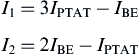
To optimize the dynamic range of D, the currents I1 and I2 are chosen as (Wang et al., 2017)
I1=3IPTAT−IBEI2=2IBE−IPTAT
(3.12)
As a final result, the duty cycle varies linearly over the temperature range. From the duty cycle D, the temperature ϑC in degrees Celsius can be calculated as
ϑC=D−0.320.00471°C=(D−0.32)×212.77°C.
(3.13)
Figure 3.8 Simplified circuit diagram of the CMOS temperature sensor.
Fig. 3.8 shows a simplified circuit diagram of the actual CMOS sensor. The IPTAT generator is a well-known core circuit (Razavi, 2001) implemented with PMOS current mirror (OP1, M4–M7) and bipolar transistors Q1 and Q2. The current-mirror PMOS transistors are identical. The BJT Q2 is implemented with three transistors in parallel, which has the same performance as a multi-emitter transistor with three emitters in parallel. Amplifier OP1 forces biasing of the bipolar transistors Q1 and Q2 at a current ratio of 1:3 of the current mirror (OP1, M1–M7). Together with the emitter-area ratio 1:3 of Q1 and Q2, this causes Q1 and Q2 to be biased at a 1:9 current density ratio. The difference between the base-emitter voltages of Q1 and Q2 amounts to ΔVBE=(kϑK/q) ln(9). Thanks to negative feedback with a high loop gain, OP1 operates in its linear region, so that its differential input voltage is virtually zero. This causes the voltage across resistor RPTAT to be equal to ΔVBE, so that the current through this resistor is a PTAT current IPTAT=ΔVBE/RPTAT (∼1μA at room temperature).
It is in a similar way that current IBE is generated. Because of negative feedback, OP2 and MOS transistor M10, together with resistors RBE1 and RBE2 operate as a voltage-to-current converter. If one of the switches SBE1 and SBE2 is ON, then amplifier OP2 and resistor RBE convert the base-emitter voltage VBE3 of Q3 into current IBE=VBE3/RBE through RBE. Although if both switches SBE1 and SBE2 are ON, the total resistance amounts to RBE/2, so that the converted current is 2IBE=2VBE3/RBE. These currents comprise part of the charge/discharge current of capacitor C. During the charge phase of capacitor C, S1 is ON and only one of the switches SBE1 and SBE2 is ON. This causes capacitor C to be charged with current I1=3IPTAT−IBE. During the discharging phase of capacitor C, switch S1 is OFF, both switches SBE1 and SBE2 are ON. This causes capacitor C to be discharged with current of I2=2IBE−IPTAT. These current values correspond with those mentioned in Eq. (3.12).
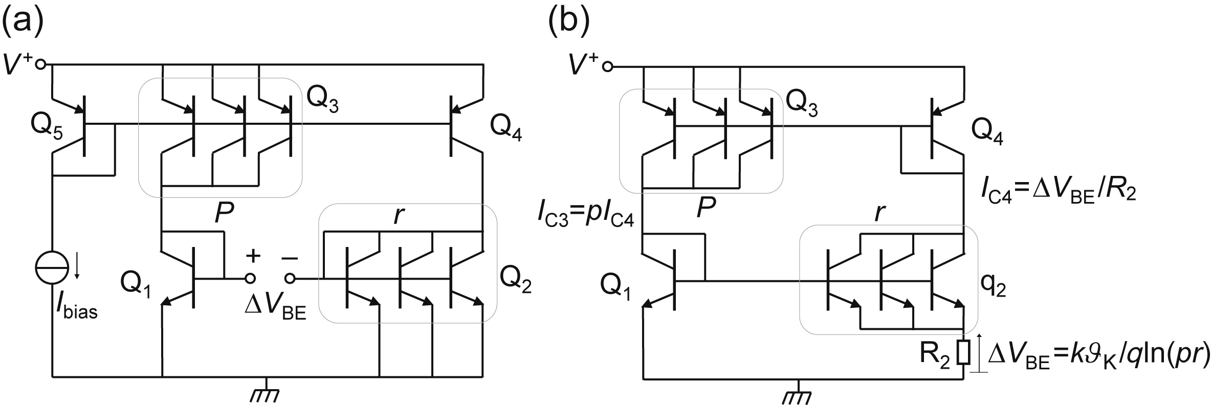
When using CMOS technology, straightforward implementation of the circuit in Fig. 3.8 would result in poor accuracy. This inaccuracy would be mainly due to the large component mismatch of the MOSFETs, which would cause not only inaccuracy in the current ratio of the current mirrors but also large offset voltages in the two op-amps. According to the concepts discussed in Section 3.5, these problems can be solved by applying DEM and chopping. Doing so yields the modified circuit of Fig. 3.9 (Wang et al., 2017).
Figure 3.9 Circuit modifications for reaching a higher accuracy, using dynamic element matching (DEM) and chopping.
Also in this improved circuit, mismatches of the input transistors of the applied amplifiers OP1 and OP2 cause large offset voltages, which are connected in series with the basic signals ΔVBE and VBE and thus directly influence sensor accuracy. To minimize this influence, the effects of offset and 1/f noise of the op-amps are mitigated by applying chopping. For the clock signals of the choppers, the output signal of the relaxation oscillator is used. Therefore, in this design no external clock is required.
Component mismatches of the current mirror transistors are also major sources of error because these mismatches influence the ratios of the currents of current mirrors. From Eq. (3.12) it can be concluded that mismatch of resistors RBE1 and RBE2 causes inaccuracy of the IBE components. Finally, from Eq. (3.6) it can be concluded that also mismatch of the emitter areas of the substrate PNPs Q1 and Q2 will affect the accuracy of the sensor. All of these errors are mitigated by applying DEM. To prevent that the DEM switches in block SB2, which are used to interchange Q1 and Q2, cause a voltage drop, Kelvin connections are used to sense ΔVBE accurately (Wang et al., 2017). Similar to the chopping state machine, the DEM states are also clocked by the output of the Schmitt trigger so that no external clock is required. When all groups of components would rotate one by one, thus obtaining each possible permutation, this would require a large number of periods. This would be quite time- and energy-consuming. Therefore, all four groups of components rotate simultaneously, within only eight DEM/chopping states. In Wang et al. (2017) it is shown that this huge simplification hardly affects the accuracy. During each DEM/chopping cycle the following actions take place
• the PMOS transistors of the current sources are rotated once,
• the four components of Q1 and Q2 are rotated twice,
• the RBE resistors are swapped four times,
• the op-amps are chopped four times.
Without further provisions, the most important source of error in the circuit (Fig. 3.9) would be related to process spread in the base-emitter voltage VBE3 of Q3 (Meijer et al., 1989). In the selected CMOS technology, the maximum deviation in this voltage amounts to about ±15mV, resulting in an unacceptable temperature error of about ±4K. This spread can be corrected by trimming both the emitter area of Q3 and the bias current. A trimming scheme has been implemented that enables trimming of the base-emitter voltage with a worst-case (i.e., largest) step size of about 50mK (Wang et al., 2017). After calibration, the trim code is stored by zapping the Zener diodes, which function as a reliable, low-cost, on-chip memory. This calibration is performed at the wafer during production and is performed at a single temperature (one-point trimming).
Via a buffer amplifier, the output signal of the Schmitt trigger is directly used as output of the smart sensor. Optimal use of this output signal requires the user to have some knowledge, as will be explained in the next section.
3.7. Signal processing of duty cycle modulated signals
3.7.1. Three methods of averaging
As described in the previous section, a DEM/chopping cycle consists of eight states. Because of component mismatches, the duty cycle of the sensor output signal will vary from period to period. In the case of constant temperature, the output signal will repeat every eight periods (Fig. 3.10). To achieve the best accuracy, the output of the sensor must be properly processed, as will be discussed in this section.
A microcontroller can measure the time intervals tL1, tH1; tL2, tH2, using its own timer, as discussed in Section 3.4.2. As discussed in the previous section, systematic errors caused by component mismatch and offset are compensated by averaging them over eight successive periods of the duty cycle modulator. This signal-processing step is performed by the user, who must, therefore, be aware that the use of incomplete DEM/chopping cycles will result in loss of accuracy, which will be demonstrated with experimental results presented in Section 3.8.1. There are various ways in which the output of the sensor can be averaged, as will be discussed here.
Figure 3.10 Output signal of the temperature sensor.
3.7.1.1. First type of averaging: best accuracy at any speed
The best accuracy is achieved by computing the duty cycle of each of the eight periods of a DEM/chopping cycle (Fig. 3.10) and then averaging the results. This yields the average value Davg1 as
Davg1=18∑8i=1tHitHi+tLi,(i=1,2…8).
(3.14)
3.7.1.2. Second type of averaging: simplest method
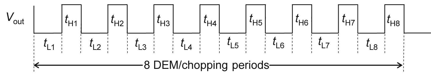
In this method, firstly the eight HIGH and LOW times are summed. Then to compute the average Davg2 only a single division is performed according to the equation:
Davg2=∑8i=1tHi∑8i=1(tHi+tLi),(i=1,2…8).
(3.15)
Because performing a floating-point division takes relatively substantial microcontroller time, this type of averaging is faster. However, it yields a higher residual second-order error. This can be explained as follows: In the calculation of Eq. (3.15), each period has a different weight. The longer periods will have larger weights than the shorter ones, and thus will contribute more to the error of the final “averaged” result. As an example, Fig. 3.11 shows the simulated residual temperature errors caused by 2mV offset in OP1 (Fig. 3.9) (worst case) for the two types of averaging: Davg1 and Davg2, respectively. Here, both residual errors have been normalized to 0 at 27°C. Note that the average Davg2 results in larger errors, especially at low temperatures. The offset voltage of OP1 is a dominant source of error, and an offset of 2mV is the worst-case value. In Section 3.8, Fig. 3.14(b), we will evaluate this further using experimental results.
Figure 3.11 Simulated residual errors obtained with Davg1 and Davg2 for an offset voltage of Vos1=2mV for OP1. Mismatch of other components is assumed to be zero.
3.7.1.3. Third method of averaging: best accuracy at intermediate and low speeds
When averaging is applied over more than one DEM/chopping cycle, a third type of averaging can be used, which also reduces the number of divisions, while still obtaining the best accuracy. This method works as follows: Suppose that the first DEM/chopping cycle of the sensor output has 16 time intervals, tL1,1, tH1,1,…tL8,1, tH8,1, according to Fig. 3.10, and that in the microcontroller these intervals are represented by the numbers NL1,1, NH1,1, NL2,1, NH2,1,…NL8,1, NH8,1, respectively. For the next DEM/chopping cycle these intervals are represented by the numbers NL1,2, NH1,2, NL2,2, NH2,2,…NL8,2, NH8,2, respectively, etc. After M DEM/chopping cycles, the duty cycle Davg3 is calculated with an equation similar to Eq. (3.14)
As compared to using Davg1 (Eq. 3.14), with this method the number of division operations is M times less, while its accuracy is almost the same. Note that this advantage is achieved for M>1 (M is an integer), and therefore only suited for slower measurement systems.
3.8. Fabrication and test results
3.8.1. Fabrication
The temperature sensor described in Section 3.6 is fabricated in a standard 0.7μm CMOS technology of ON-Semiconductor (Fig. 3.12(a)). Most of the pads are used to store the trimming code needed for wafer-level calibration and to perform trimming. These pads are not accessible for the user. The chip also has three pads available for the user, which are VCC, GND, and OUT.
The sensor chips are available in a variety of packages (TO18, TO92, TO220, SOT223, and SOIC-8).
The output signal of the sensor is a rail-to-rail square-wave voltage (Fig. 3.10) with a frequency that varies from about 500Hz to 7kHz. Only the duty cycle of the square waves provides accurate temperature information. As explained in Sections 3.5–3.7, DEM/chopping is applied. To benefit from this, the duty cycle Davg should be calculated over eight successive periods in one of the three ways described in Section 3.7. To find the temperature ϑC in degrees Celsius, the value of Davg is substituted in Eq. (3.13).
Figure 3.12 (a) Chip photograph, (b) temperature sensor in a variety of packages. Reproduced by permission of Smartec.
To show the importance of averaging over groups of eight periods, the solid line in Fig. 3.13 shows the moving average of the measured results using Eq. (3.14). At this scale of the graph, no fluctuations are seen. Yet, when depicting all measurements for each period separately, without any averaging (dashed line in Fig. 3.13), huge fluctuations are found, which are because of mismatch of the CMOS components, as discussed in Section 3.6. With the dashed line, the results repeat every eight readings. Obviously, this implies systematic errors that correspond to the eight states within each DEM/chopping cycle. These errors vary from −4.0°C to 3.7°C, and these values vary from chip to chip, depending on the specific mismatches. Averaging over eight periods reduces these systematic errors to less than 0.02°C. At the scale used for this figure, no fluctuations due to noise can be seen because these fluctuations are rather small. Yet, these small fluctuations are important too and will be discussed in detail in Section 3.8.3.
Figure 3.13 Measured temperature reading at room temperature (ϑC,ref=25.356°C). DEM, dynamic element matching.
The measurement can be started at any arbitrary transient (upward or downward) in a DEM/chopping cycle. Any series of eight periods will cover a full DEM/chopping cycle. The measurement results discussed in the rest of this chapter are all based on using the average over an integer number M DEM/chopping cycles. On the other hand, it should be noted that for M≫1, errors due to using incomplete DEM/chopping cycles (so M is no longer an integer) rapidly decrease with an increasing value of M. This also means that simple analog circuits, as will be discussed in Section 3.8.6, and digital systems with a low acquisition rate can still offer rather good accuracy.
3.8.2. Accuracy over temperature range and supply voltage range
Fig. 3.14(a) shows a typical result of measured systematic errors over the full temperature range of −45°C to 130°C. The average duty cycle has been calculated according to Eq. (3.14) (Davg1). With Eq. (3.16) almost the same result was found. The figure shows that there is still some systematic nonlinearity. For low temperatures, this is mainly because of an incomplete curvature correction. For high temperatures this is because of the exponential increase in leakage currents.
Fig. 3.15(b) shows the measured total error for the case that, with the same empirical data, the average duty cycle (Davg2) is calculated with the simpler Eq. (3.15). At low temperatures, applying Davg2 results in more error than when using Davg1 or Davg3, which confirms the analysis presented in Section 3.7.1.2. On the other hand, for the temperature range 0–110°C, the differences between Fig. 3.14(a) and (b) are negligible.
Figure 3.14 Systematic errors versus temperature for 90 samples taken from two batches, when the duty cycle is calculated with (a) Eqs. (3.14) or (3.16) (Davg1 or Davg3) or with (b) Eq. (3.15) (Davg2). Note that (a) and (b) concern the same experimental data.
Figure 3.15 Measured resolution (standard deviation) versus measurement time (72MHz sampling frequency). Reproduced by permission of IEEE.
When using the analog output features of the sensor (see Section 3.8.6), the results are similar to those shown in Fig. 3.14(b).
With a supply voltage varying from 2.5 to 5.5V, the measured output variations were less than 0.1°C (Wang et al., 2017).
3.8.3. Noise
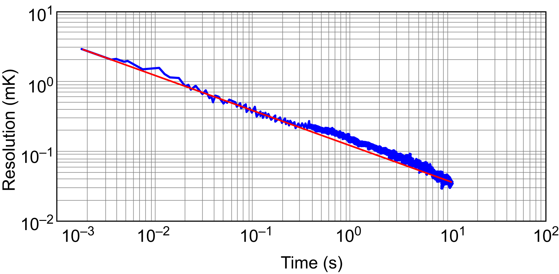
To measure the noise of the sensor its temperature has been kept at a (very) stable value of about 25°C. Noise measurements with a standard deviation as low as 30μK (=30×10−6°C) take special care and is only possible when the temperature is very stable during the measurement. To realize this, the sensors were assembled in a thermal buffer with a significant thermal time constant. In additional to that, a special measurement technique is applied to eliminate the effects of change in the environmental temperature (Wang et al., 2017). Each measurement was based on averaging over an integer numbers M of DEM/chopping cycles.
Fig. 3.15 shows that the standard deviation of the noise lowers with the square root of the measurement time. This behavior should be expected for thermal noise, but not for 1/f noise. This means that the suppression of 1/f noise works sufficiently well. For a measurement time tm of 1s (555 DEM cycles of 8 periods, M=555), the resolution is about 0.17mK (rms). For the minimum measurement time tm of 1.8ms (8 periods, M=1), the resolution is about 3mK (rms) (Fig. 3.15). According to Makinwa (2010), the energy efficiency of the sensor can be characterized with a resolution figure-of-merit (FoM) F, which is defined as
F=E⋅s2,
(3.17)
where E is the energy that is consumed during a single measurement (a single DEM cycle) and s is the resolution of the sensor, which corresponds to the standard deviation of its noise in K. With a supply voltage of VCC=3.3V, a supply current of Isupply=60μA, and a measurement time of tm=1.8ms (for eight periods), the energy consumption E for a single measurement amounts to 356nJ. Substitution of these values in Eq. (3.17) yields a resolution FoM F=3.2pJK2, which is much better than that of other BJT-based sensors on the market (Wang et al., 2017).
3.8.4. Packaging shift and long-term stability
In precision temperature sensors, variation in mechanical stress is the main cause for long-term drift. This also holds true for the smart temperature sensors discussed in this chapter. In BJT-based temperature sensors, the sensitivity to mechanical stress is due to the so-called piezo-junction effect, the effect that causes the base-emitter voltage of bipolar transistors to be stress-sensitive (Fruett and Meijer, 2002). This effect is anisotropic, i.e., it depends on the orientation of the mechanical stress and the direction of the collector current with respect to the crystal orientation (Creemer et al., 2001; Fruett and Meijer, 2002). For PNP transistors, this effect is less significant than for NPN ones, whereas for tensile stress the effects are less significant than for compressive stress. Thorough investigations of these effects show that the best choice for BJTs as temperature sensors is to select vertical PNP transistors fabricated in {100}-oriented silicon wafers (Fruett and Meijer, 2002). This fits very well with common CMOS technology. With respect to the packaging technologies listed in Section 3.8.1, the best results were obtained with TO-18 packages. Long-term stability tests show that over a period of more than 1year the measured drift3 was less than 2mK.
3.8.5. Performance summary
The main features of the smart BJT-based temperature sensor discussed in this section are listed in Table 3.2. More specifications of the final product, called SMT172, can be found elsewhere (Smartec, 2016b). The main achievements of this product concern high accuracy and resolution and an excellent resolution FoM. The measurement time can be as low as 1.8ms, which corresponds to the time needed for a single DEM/chopping cycle of eight periods. One of the main reasons for the low-energy consumption of the sensor is that it outputs a quasi-analog signal. The time intervals of which are then digitized by a microcontroller and not in the sensor. So, shifting some functionality from the sensor to the microcontroller helps to reduce self-heating in the sensor and to reduce system costs.
Table 3.2
Main features of the smart bipolar junction transistor–based temperature sensor
Name
SMT172
Supply voltage (V)
2.7–5.5
Supply current (μA)
42–75
Number of pins
3
Temperature range (°C)
−45 to 130
Output signal
Duty cycle modulated
Minimum measurement time (ms)
1–22
Supply voltage sensitivity (°C/V)
0.1
Best accuracy (°C) (Temperature range [°C])
0.1 (−20 to 60)
0.3 (−45 to 130)
Resolution at measurement time
0.00017°C at 1s
0.003°C at 1.8ms
3.8.6. Simple systems with digital and analog signal processing
An attractive feature of temperature sensors with DCM output, such as the SMT172, is that the output signal can be read in both a digital and an analog way. Two simple system examples of each are discussed here:
Example 3.2: Temperature monitoring system with digital signal processing
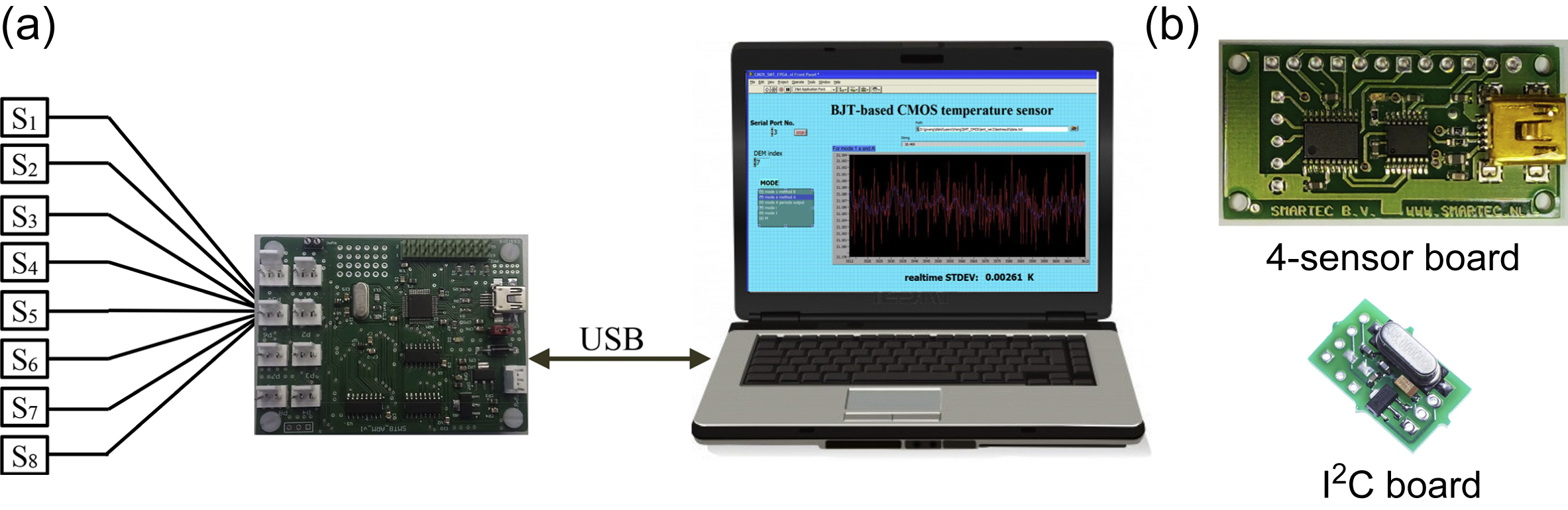
Fig. 3.16 (a) shows an eight-sensor monitoring system with digital signal processing, which consists of
• eight sensors,
• an evaluation board SMT8-ARM (Smartec, 2016b), which can read the output signals of up to eight sensors,
• a computer.
This system can monitor temperatures at eight locations. The signals are processed as discussed in Sections 3.4.2 and 3.7. The evaluation boards have been developed for rapid prototyping and are provided with the required microcontroller software, thus lowering the threshold for new users in evaluating the features of the sensors for their application. Similarly, other evaluation boards have also been developed (Fig. 3.16(b)), such as a board with an I2C interface, which enables up to 128 sensors to be measured in one system.
Example 3.3: Temperature control system with analog signal processing
An example of using the analog sensor properties with a DCM output signal is shown in Fig. 3.17. This figure shows a control circuit for a simple analog thermostat, where a smart temperature sensor with a duty-cycle-modulated output (Fig. 3.4) senses a temperature to be controlled. When duty cycle D varies linearly with temperature and a low-pass filter is applied, the output voltage Vaverage of that filter is a DC voltage that varies linearly with temperature. In this setup, Vaverage is compared with the set-point voltage Vsetpoint, which is adjusted with a potentiometer. The binary output voltage of the Schmitt trigger is used to control a heater (not shown in Fig. 3.17), which is provided with power as long as Vaverage<Vsetpoint. Note that both voltages Vaverage and Vsetpoint are also proportional to the supply voltage. However, this will not affect the binary output of the Schmitt trigger. Note also that no microcontroller is needed to implement such a processor.
Figure 3.16 (a) Eight-sensor measurement system, (b) Other evaluation boards. Reproduced by permission of Smartec.
Figure 3.17 Sensor part of a simple thermostat, with a smart temperature sensor with duty cycle modulated output voltage Vo and a potentiometer to adjust the set point. The output of the Schmitt trigger controls a heater (not shown in this figure).
The way the filter is used to average is similar to that presented in Section 3.7.1.2 for digital signals. This means that within a DEM/chopping cycle, long periods have more influence than short ones. According to Fig 3.14, it should be expected that at low temperatures the error will increase. On the other hand, for the temperature range from 0°C to 110°C the results will be as accurate as those obtained with other ways of averaging.
3.9. Summary
In industrial applications, precision is often more important than accuracy, whereas precision requirements are often only valid for a limited period time. When designing or purchasing a temperature sensor system, it is important to start with a target list of requirements and to distinguish short- and long-term drift on the one hand and resolution, precision, and accuracy on the other.
For smart sensors and MEMS, the most common temperature-sensing elements are transistors, thermocouples, and thermopiles because these elements can be implemented with IC technology. At the system level, also Pt resistors, thermistors and IR sensors are important. A comparison between the properties of four types of sensing elements is presented. Thermopiles are used to measure temperature differences and are very suited for thermal sensors, which measure a physical quantity by transducing the signals into thermal quantities first, and then transducing the thermal quantities into electrical quantities. Usually, in such sensors a reference temperature is also measured, for instance, with a bipolar transistor.
For the temperature range of −55°C to 150°C, BJTs are very suited to be used as temperature sensors because of their low cost, good long-term stability, and high sensitivity. These transistors can also be fabricated in standard Bipolar, BICMOS, and CMOS technology, together with analog and digital electronic circuits. For these reasons, for many smart sensors and MEMS, these elements are preferred when implementing temperature-sensor systems.
The main properties of BJTs applied as temperature sensors are summarized. In addition to the direct use of the base-emitter voltage, the difference between two base-emitter voltages of transistors is also used as a measure for temperature. In the latter case, a voltage is obtained that is PTAT. Base-emitter voltages together with PTAT voltages can be used as measures for temperature and to generate a (bandgap) reference voltage as well. Based on physical properties, the sensor characteristics can be calibrated and adjusted, using single-point trimming at, for instance, room temperature. This feature is very useful for the design and fabrication of integrated smart temperature sensors.
It is shown that even low-cost CMOS technology can be very suited to realize high-precision temperature sensors and bandgap voltage references. Vertical PNP transistors, such as the substrate transistors in common CMOS {100}-oriented silicon wafers, are sufficiently immune to the effects of mechanical stress. Therefore temperature sensors using these BJTs have less packaging shift and good long-term stability. In CMOS technology, component matching is poor. Notwithstanding this drawback, methods are available to achieve high accuracy with analog circuits implemented in CMOS technology. These methods, such as DEM and chopping, appear to be very effective in reducing or even eliminating the effects of CMOS components mismatch.
These concepts have been applied in a smart temperature sensor with a DCM output signal, which is presented as case study. It is shown that with such smart sensors a high reliability and accuracy can be obtained at low costs. Moreover, the energy consumption of these sensors can be very low, which is important for limiting self-heating. DCM output signals are not only suited for direct readout by a microcontroller but can also be used in analog applications, without any microcontrollers or digital circuitry.
It is demonstrated that (1) thanks to the applied concepts, such as DEM and chopping, very high accuracy, and precision is achieved, (2) thanks to the applied PNP transistors, which are sufficiently immune to mechanical stress, a good long-term stability is achieved, and (3) thanks to the application of duty-cycle modulation, the sensors consume very little energy. Measurement results show that the presented BJT-based temperature sensor achieves a state-of-the-art resolution FoM, which amounts to 3.2pJK2 at room temperature. This makes this sensor highly suited for low-energy applications. After wafer calibration at room temperature, the accuracy of the sensor is better than 0.1°C (−20°C to 60°C) and 0.3°C (−45°C to 130°C), respectively. Package-induced errors were found to be less than 0.1°C at room temperature.


 (3.12)
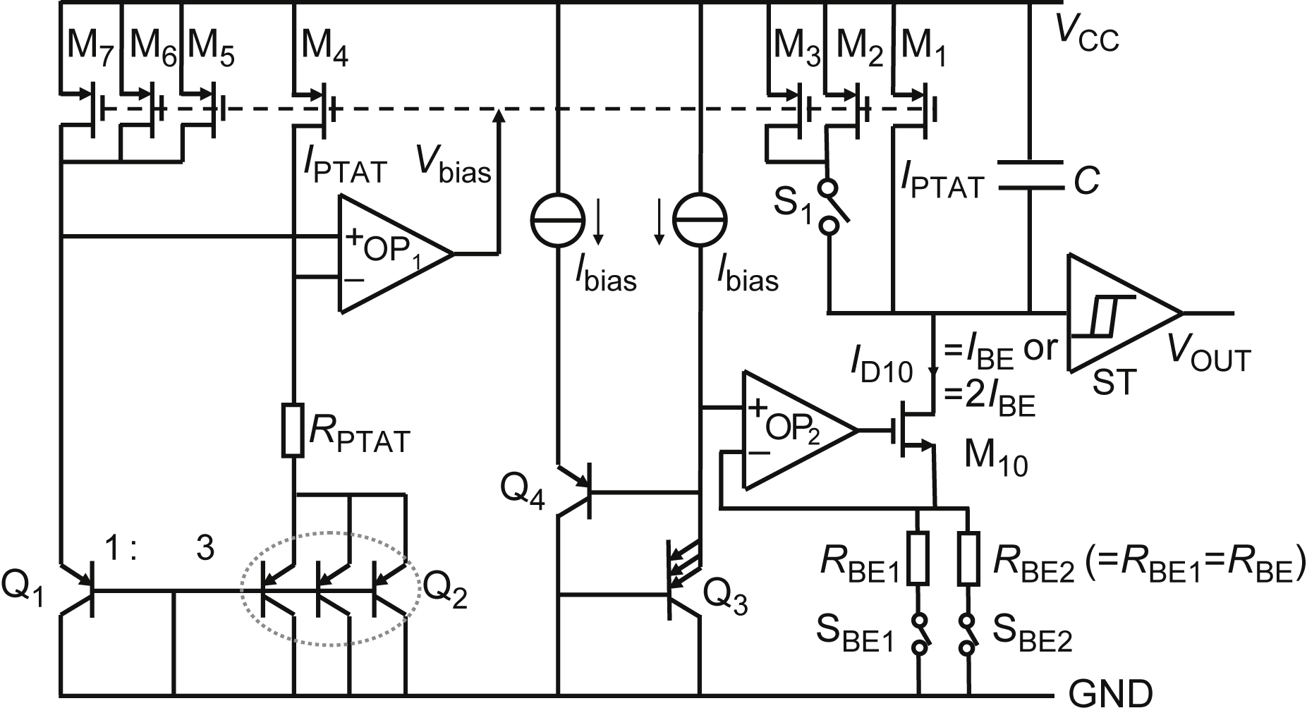

 (3.14)
 (3.15)
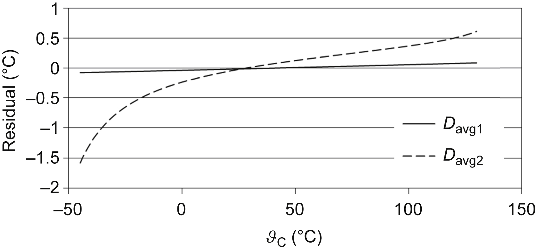
 (3.16)