
Basic Programming Techniques
Joe Hamman Director, Platform Software Solutions at Integrated Computer Solutions, Waltham, MA, United States
Abstract
This chapter will present the details and techniques needed to create, build, and deploy a basic, embedded runtime image. We will first review the technical details of a popular, low-cost embedded reference platform, focusing on system initialization. We will walk through the installation of the software development kit for the board along with the steps needed to build, download, and run a program that exercises digital I/O by toggling an LED. We will then build and deploy a simple runtime image that prints characters using the serial port (UART) in polled I/O mode. Following an overview of hardware interrupts and interrupt handlers, we will build and deploy a timer application using interrupts.
Keywords
Embedded platform; Reference board; LED; UART; Reset; Initialization; Timer; Digital I/O; Interrupts
1 Introduction
The best way to learn embedded programming is through hands-on training. In this chapter, we will provide the basic techniques needed to create, cross-compile, and run programs on a common reference board. Many people learn to program natively on a PC or workstation, where the host operating system performs many actions “behind the scenes.” On these host platforms, the operating system handles the housekeeping activities performed when loading and executing programs. The operating system also restricts access to hardware registers, storage devices, and communication channels. These operations are usually performed by calling privileged operating system functions or accessed via device drivers.
To effectively develop software for embedded systems, one must understand these “behind the scenes” actions. This is a requirement when programming systems without an operating system—often referred to as “bare metal” designs. While not required to program a system running a rich operating system like Linux, understanding these concepts will help one make efficient architectural decisions and assist with low-level debugging when needed. The first place to start is with the hardware platform details.
2 Reference Platform Overview
There are many quality, low-cost platforms available to learn on. We will use the FRDM-KW41Z reference board from NXP Semiconductor (Fig. 1). This is a low-cost board using the NXP KW41Z512VHT4 System on Chip (SoC) device. This SoC contains an ARM Cortex-M0 + CPU along with an assortment of on-chip subsystems. These subsystems include serial ports, I/O ports, timers, and other devices commonly used in deeply embedded devices. In addition to the SoC, the platform also contains flash and RAM memory, along with the signal conditioning circuitry and connectors needed to support the on-chip I/O devices. The design also contains an onboard JTAG debugging interface, making it easy to download and debug programs without the need for additional tools.

2.1 Understanding Hardware
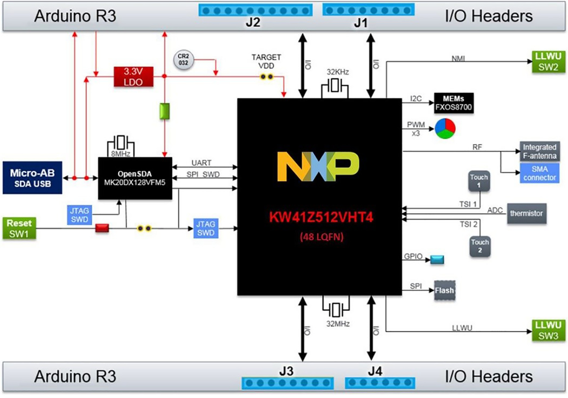
To fully understand the details of an embedded platform, there are two documents that are required. The first is the platform User’s Guide. This document contains the details needed to initialize the platform and access peripherals. It typically contains the platform block diagram, reset details, board schematics, and connector pinouts. Fig. 2 shows the block diagram of the FDRM-KW41Z board we will be using.
The second document required is the processor data sheet. For this platform, it is the reference guide for the NXP KW41Z/31Z/21Z family of devices. Many times, these reference guides will refer to additional documents, like the CPU architecture data sheet. These additional documents will contain hardware-specific details, such as voltages and frequencies, bus timing, and any low-level details applicable to the system reset, system initialization, clocking, etc.
Properly initializing the system requires intimate knowledge of both hardware and software. If even one detail is overlooked or incorrect, the system may not function. Embedded hardware providers have added features to help with this phase of a project. Preconfigured initialization code is usually included in embedded software development kits (SDKs). For reference platforms like the one we are using, this is usually the easiest way to learn how to initialize a board from reset and how to program the peripherals. These documents, software development kits, and sample runtime code are available on the NXP website. For this chapter, the SDK we will use is the NXP MCUXpressoIDE.
3 SDK Installation
The coding examples given in this chapter will only run on the previously mentioned NXP reference board. The easiest way to build and run these examples is to use the NXP SDK. In addition to the required cross-development tools (C compiler, linker, debugger, etc.), the SDK provides a rich set of header files, libraries, and sample projects. These files provide utility functions to configure and use the peripherals contained in the device. The SDK also contains powerful project wizards that allow the developer to easily build simple and complex projects.
3.1 Download and Installation
NXP’s MCUXpresso Software Development Kit (SDK) can be found online at http://www.nxp.com/mcuxpresso/sdk. Click on the “Download” link and follow the steps to download and install the SDK. If prompted, the board being used is the FRDM-KW41Z.
3.2 Building a Project
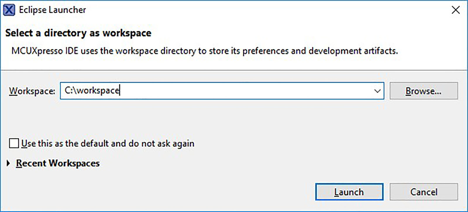
Once the SDK is installed, launch the SDK and provide the location of the workspace directory you would like to use or select the default location provided (Fig. 3).
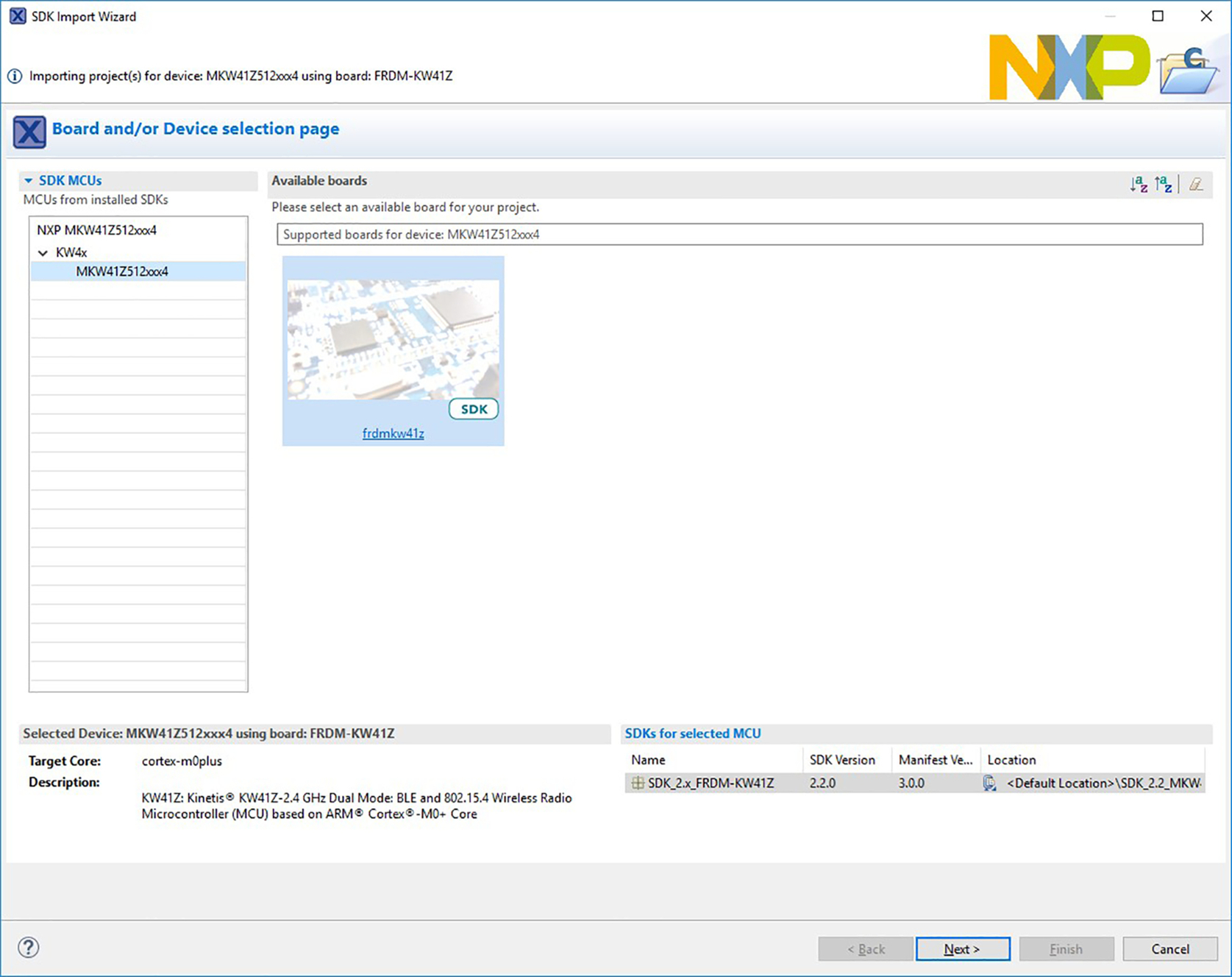
To import the example project, locate the MCUXpresso IDE–Quickstart Panel and select “Import SDK example(s) ...” When the SDK Import Wizard opens, expand the KW4x group in the list of SDK MCUs and make sure the MKW41Z512xxx4 is highlighted and click Next (Fig. 4).
On the second page of the SDK Import Project Wizard, expand the driver_examples group, then expand the gpio group, select the led_output example and click Finish (Fig. 5).

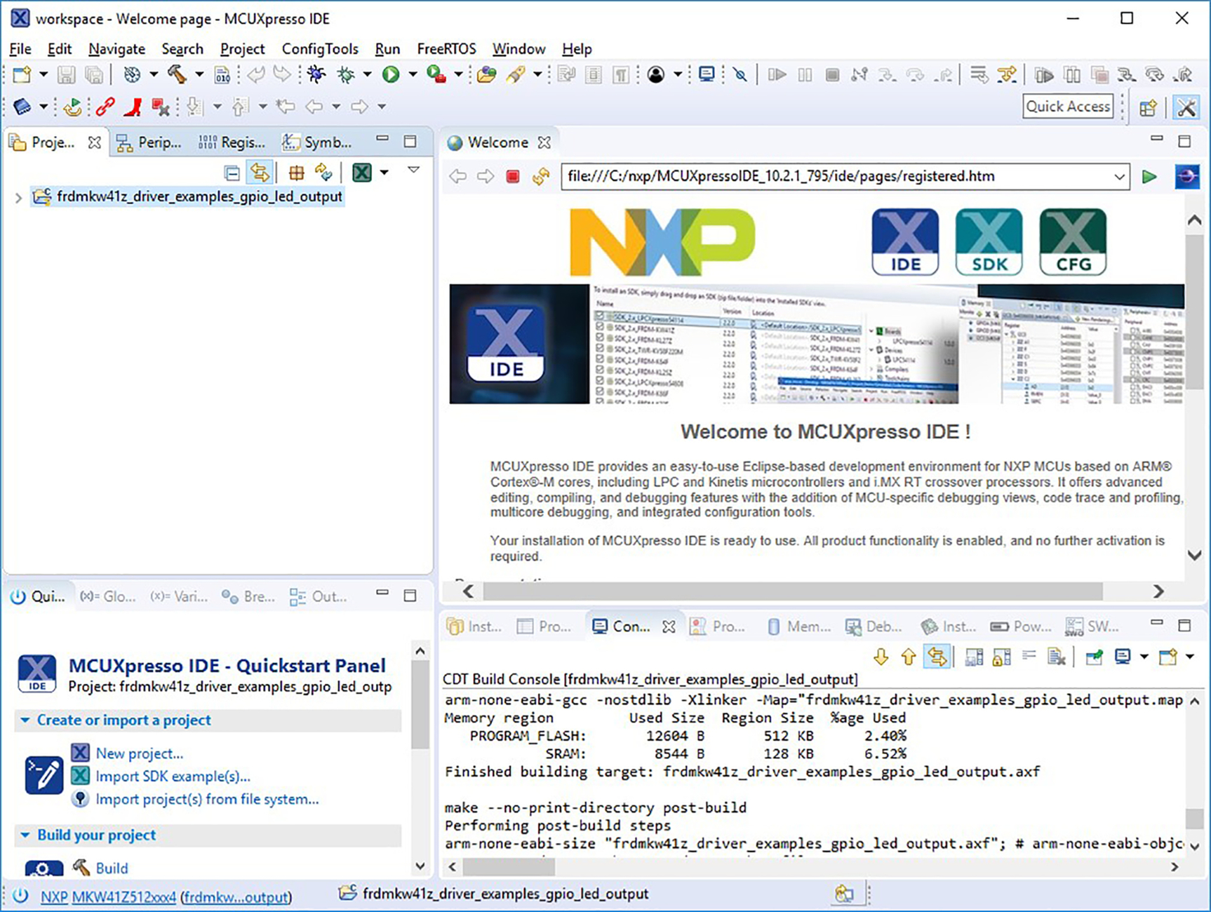
Before building the project, make sure the Console tab is selected so the build output will be visible. To build the project, right-click on the project name in the Project Explorer view and select “Build Project” from the pulldown menu. Build output should be visible in the console view (Fig. 6).
3.3 Debugging the Project
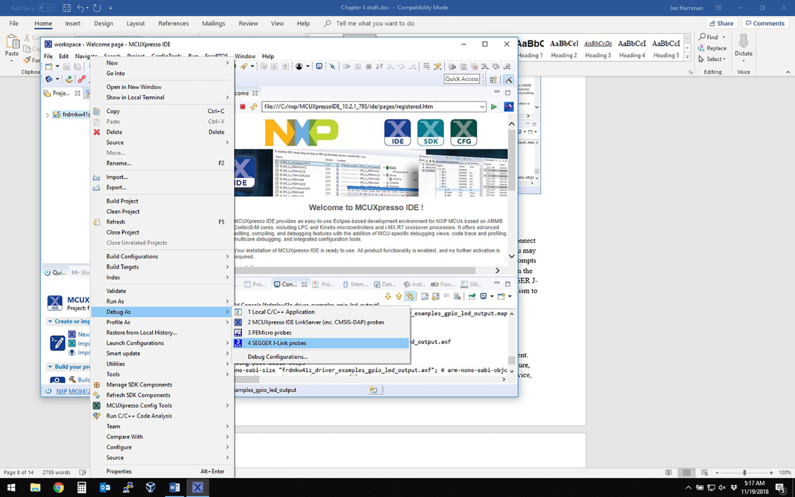
To download and debug the example program, we will use a JTAG debug connection. Connect the reference board to your workstation using the USB cable supplied with the board. You may be prompted to install device drivers to support the JTAG connection. If so, follow the prompts or see the SDK documentation. With the board connected, right-click on the project in the project explorer and select “Debug As >”. From the second pulldown menu select “SEGGER J-Link probes” (Fig. 7).
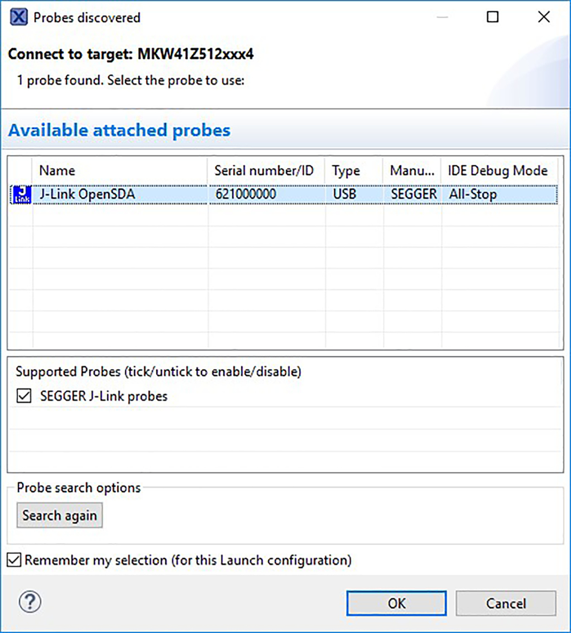
A window may appear with a list of JTAG probes attached to the workstation. The default options can be used and click on OK (Fig. 8).
The debugger in the SDK will reset the target processor, download the binary image to the target, insert a temporary breakpoint at main(), and release the processor from reset. The processor will execute the startup code described earlier (memory and variable initialization, etc.) and then halt execution at the temporary breakpoint at main(). At this point the debugger IDE can be used to single step, set breakpoints, examine variables, etc. To execute the program at full speed, press the “F8” function key. The red LED on the board should begin flashing. To terminate the debug session, press the “CTRL-F2” key.
4 Target System Configuration and Initialization
4.1 System Reset
All embedded processors have a well-defined mechanism to handle the power-on reset event. However, the details of these mechanisms will vary based on many factors: CPU architecture, SoC manufacturer, and a long list of optional settings. These settings specify the boot device, bus settings, single-chip mode, clock sources, etc. There are also many ways these settings can be implemented. One way is to use pull-up resistors on specific I/O or bus pins. These pins are read shortly after reset and determine the optional settings for that SoC. After the settings are determined, these pins assume their primary functions. Another method employed on some SoCs is to read the settings from a specific location in flash memory.
Once the processor has come out of reset with the correct configuration, the boot software is then required to initialize many different subsystems. These initialization steps will be very specific to the SoC being used, the way the device is configured, and which peripherals will be needed by the operating system and/or application software.
There are several sources that provide working examples of boot software. These examples can often be found in the semiconductor supplier’s SDKs, commercial RTOS vendor’s SDKs, and open source projects like Linux (www.yoctoproject.org) and FreeRTOS (www.freertos.org). Reading sample boot code operations and identifying the appropriate sections in the previously mentioned documentation is an excellent way to learn how a reference platform like the FDRM-KW41Z is configured and initialized at boot time.
The NXP SDK boot code takes a minimal approach and only does a few things before calling main(). It disables interrupts, turns off the watchdog timer, initializes the .data sections in RAM, initializes the .bss section in RAM to all zeros, enables interrupts, then calls main(). Here is the code snippet that performs these operations:
- void ResetISR(void) {
- // Disable interrupts
- __asm volatile ("cpsid i");
- // Disable Watchdog
- // SIM->COPC register: COPT = 0,COPCLKS = 0,COPW = 0
- *((volatile unsigned int *)0x40048100) = 0x00u;
- // Copy the data sections from flash to SRAM.
- unsigned int LoadAddr, ExeAddr, SectionLen;
- unsigned int *SectionTableAddr;
- // Load base address of Global Section Table
- SectionTableAddr = &__data_section_table;
- // Copy the data sections from flash to SRAM.
- while (SectionTableAddr < &__data_section_table_end) {
- LoadAddr = *SectionTableAddr ++;
- ExeAddr = *SectionTableAddr ++;
- SectionLen = *SectionTableAddr ++;
- data_init(LoadAddr, ExeAddr, SectionLen);
- }
- // At this point, SectionTableAddr = &__bss_section_table;
- // Zero fill the bss segment
- while (SectionTableAddr < &__bss_section_table_end) {
- ExeAddr = *SectionTableAddr ++;
- SectionLen = *SectionTableAddr ++;
- bss_init(ExeAddr, SectionLen);
- }
- // Reenable interrupts
- __asm volatile ("cpsie i");
- main();
- // main() shouldn't return, but if it does, we'll just enter an infinite loop
- while (1) {
- ;
- }
- }
These steps are performed for any system using the “C” programing language and they represent some of the “behind the scenes” steps mentioned in the introduction to this chapter. While this section of code performs the bare minimum to initialize the programming environment, it does nothing to initialize the I/O devices used in the examples we will present in this chapter. Many real-world implementations also include systemwide hardware initialization steps in this section. Other implementations choose to defer the hardware initialization and perform it later in a section of code dedicated to a specific hardware subsystem. It is very common to see a combination of the two—systemwide initialization being done very early in the boot code and initialization for a specific subsystem being performed later when the associated device driver is initialized. Regardless of when the hardware initialization occurs, it starts with the Clock and I/O subsystem initialization.
4.2 Clock Configuration
The clocking subsystems on modern embedded SoCs are very complex. Chapter 5 of the KW41Z Reference Manual contains the detailed information needed to properly configure the clocks. Fig. 9 shows the clocking diagram.
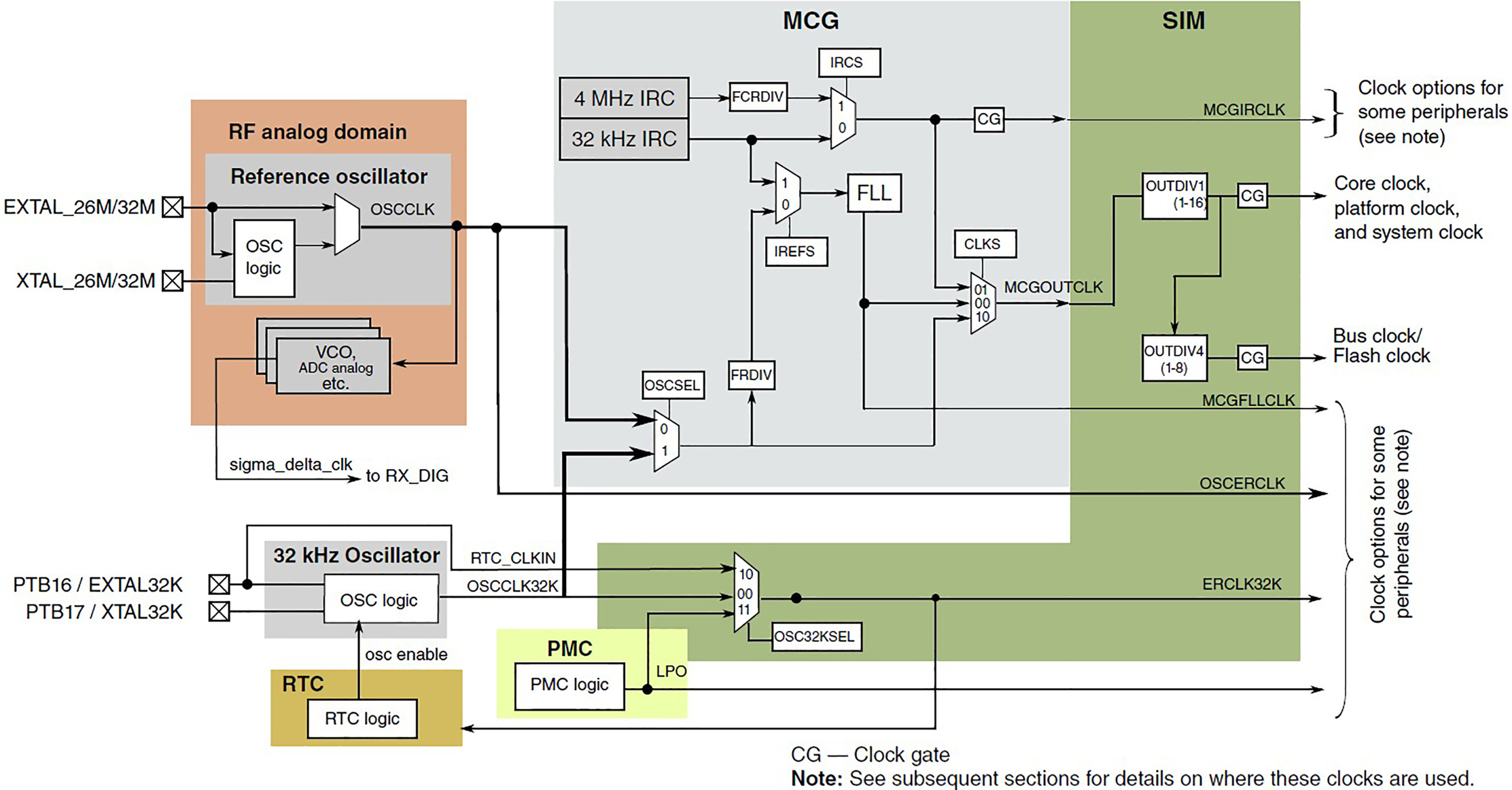
The clocking configuration on this device is a good example of a subsystem that uses a flash memory configuration mechanism. The clock dividers are initialized at reset based on the values in the FTFA_FOPT register (located in flash). When the flash is in its erased state (all bits are set to 1), bits are set in the FTFA_FOPT register and select the fast clocking mode. The developer has the option of programming the bits in flash to 0 and defaulting to a slower clocking mode. See section 5.5.1 in the reference manual for details.
The default clock settings do not enable clocking to the I/O subsystems. For the examples in this chapter, the clocking must be enabled by the application program. In the example program that blinks the red LED, the clocking to the GPIO module is enabled using a library call.
CLOCK_EnableClock(kCLOCK_PortC); /* Port C Clock Gate Control: Clock enabled */
4.3 I/O Pin Configuration
Modern embedded SoCs may also contain very sophisticated I/O capabilities. To maintain flexibility and accommodate the needs of different designs, many of the I/O pins can be configured to perform one of multiple functions. These options can be general purpose input, general purpose output, or a dedicated function associated with a specific subsystem. Two examples of dedicated functions are the transmit data signal of a serial port (UART) and a timer enable signal. If the pins associated with a specific peripheral are not used, they are often configured to function as a digital input or output. In this case, the function would be defined by the developer. Adding to the configuration complexity, many SoCs multiplex multiple dedicated functions to a single pin. It is common to see devices that have as many as six or more functions multiplexed to a single I/O pin. An example of this multiplexing can be seen in section 2.2 of the KW41Z reference manual.
There are many dependencies and restrictions on selecting specific pins for a given pin function. Sometimes a peripheral (I2C, UART, Timer, etc.) may be able to use several different sets of pins, but sometimes only a subset of the device signals can be mapped to I/O pins. A common example of this can be found in UART devices. Using one set of I/O pins, the UART exposes only the transmit and receive signals. When using an alternate set of I/O pins, the UART exposes the hardware handshake signals in addition to the transmit and receive signals.
One example from the reference manual is the CLKOUT pin for the I2C port, I2C0_SCL. This function can be found on processor pin 16 and again on pin 48 (Table 1). The first two columns identify the pin designator for two different package types. By writing specific values to the configuration registers, the physical pin can be connected internally to one of eight alternate functions (ALT0–ALT7).
Table 1
| KW41Z (48 LGA/Laminate QFN) | KW41 (WLCSP) | Pin Name | DEFAULT | ALT0 | ALT1 | ALT2 | ALT3 | ALT4 | ALT5 | ALT6 | ALT7 |
|---|---|---|---|---|---|---|---|---|---|---|---|
| 16 | J6 | PTB0 | DISABLED | PTB0/LLWU_P8/XTAL_OUT_EN | I2C0_SCL | CMP0_OUT | TPM0_CH1 | CLKOUT | |||
| 48 | C8 | PTC19 | DISABLED | TSI0_CH7 | PTC19/LLWU_P3 | SPI0_PCS0 | I2C0_SCL | LPUART0_CTS_b | BSM_CLK | BLE_RF_ACTIVE |

To help developers determine the best pin multiplexing configuration for a given design, many of the semiconductor vendors offer configuration tools. These design tools allow the developer to select a specific device, usually by part number, and then choose the subsystem settings at the feature level. These subsystems correspond to the on-chip devices shown in the SoC block diagram. The tool allows the developer to enable/disable specific peripherals, select clock sources, enable or disable features within the subsystem, and generate the required configuration files. Some vendor tools even generate boot code, header files, and basic driver functions to match the configuration. The tool provided by NXP for the KW41Z is the MCUXpresso Config Tool. Fig. 10 shows an example of this tool.

4.4 I/O Pin Initialization
For the basic hello world example contained in the SDK, a subroutine called BOARD_InitPins() calls routines to easily setup the port pins needed to send ASCII data through the serial port (UART).
PORT_SetPinMux(PORTC, PIN6_IDX, kPORT_MuxAlt4); /* PORTC6 (pin 42) is configured as UART0_RX */PORT_SetPinMux(PORTC, PIN7_IDX, kPORT_MuxAlt4); /* PORTC7 (pin 43) is configured as UART0_TX */
The routine PORT_SetPinMux() and the constants PORTC and PINx_IDX come predefined for the family of KW41Z devices. The constant kPORT_MuxAlt4 tells the routine to select the pin function shown in the Alt4 column of Table 2.1 in the KW41Z reference guide.
While the vendor configuration tools do a great job simplifying the details related to pin multiplexing, it is always a good idea to review all the details related to the I/O pins you will be using. Many of the options available on different pins are the pin direction (input vs. output), enable internal pull-up resistor, interrupt enable, edge vs. level activation, etc. It is also important to validate the internal connections selected while configuring a hardware subsystem, understand the dependencies and restrictions, and follow specific initialization sequences as recommended by the manufacturer.
It is also important to read any errata documentation that may be available. These documents tend to capture configuration, sequencing, limitations, and side effects that were unknown or not fully characterized when the SoC was initially released to production. The errata will identify these items as they relate to a specific silicon revision of the device. If your software is required to run on various silicon revisions of the SoC, your code may need to query the SoC registers containing the silicon version details and behave as required.
4.5 SDK I/O Helper Routines
Programming the registers on a modern, complex SoC can be very complex. Let’s look at a portion of code that enables clocking to the I/O port used for the LED signal:
temp = *(unsigned int *)(0x40048038); /* Read System Clock Gating Control Register 5 (SIM_SCGC5) */
temp |= 0x800;     /* Enable clocking to PORTC */
*(unsigned int *)(0x40048038) = temp; /* Write the new value to the control register */
Trying to understand code written this way requires one to switch back and forth between the programming manual and the hardware reference manual. The details can be found in section 12.2.8 of the reference manual. To make the code more manageable, many developers will replace the hardcoded constants with #define values:
#define SIM_SCGC5 (unsigned int *)0x40048038
#define PORTC_ENABLE 0x800
temp = *SIM_SCGC5;      /* Read System Clock Gating Control Register 5 (SIM_SCGC5) */
temp |= PORTC_ENABLE; /* Enable clocking to PORTC */
*SIM_SCGC5 = temp;      /* Write the new value to the control register */
This method works well but can be difficult to maintain. This is especially true when writing code that is required to support multiple variants of an SoC family that may have slightly different bitfield definitions for the same subsystems. To address this, semiconductor vendors provide files that contain various data type definitions, data structures, and routines that can be used to manage the hardware.
Here is the same portion of code using the definitions supplied by the semiconductor manufacturer:
CLOCK_EnableClock(kCLOCK_PortC); /* Port C Clock Gate Control: Clock enabled */
For our first example, blinking an LED, we will program the hardware registers using hardcoded definitions. For the remaining examples, we will take advantage of the high-level definitions provided in the SDK.
5 Programming Examples
5.1 General Purpose I/O—Blinking LED
This example simply blinks an LED repeatedly. The initialization steps are very simple:
- - Enable clocking to the GPIO port containing the LED signal.
- - Configure the pin multiplexing to allow the LED signal to be a GPIO output.
- - Initialize the GPIO port bit to turn off the LED.
- - Enable the GPIO port bit as an output signal.
- - Loop forever, toggling the LED signal.
To build and run this example in the SDK, follow these steps:
- - Close any existing projects.
- - Select File | New | Project…
- - Expand MCUXpresso IDE and select New C/C ++ Project, click Next.
- - Select the MKW41Z512xxx4 MCU and click Next.
- - In the SDK Wizard, change the project name (optional), unselect all the checkbox options except baremetal, select “Empty board files,” unselect both “CMSIS-Core” and “Import other files,” then click Next (Fig. 11).
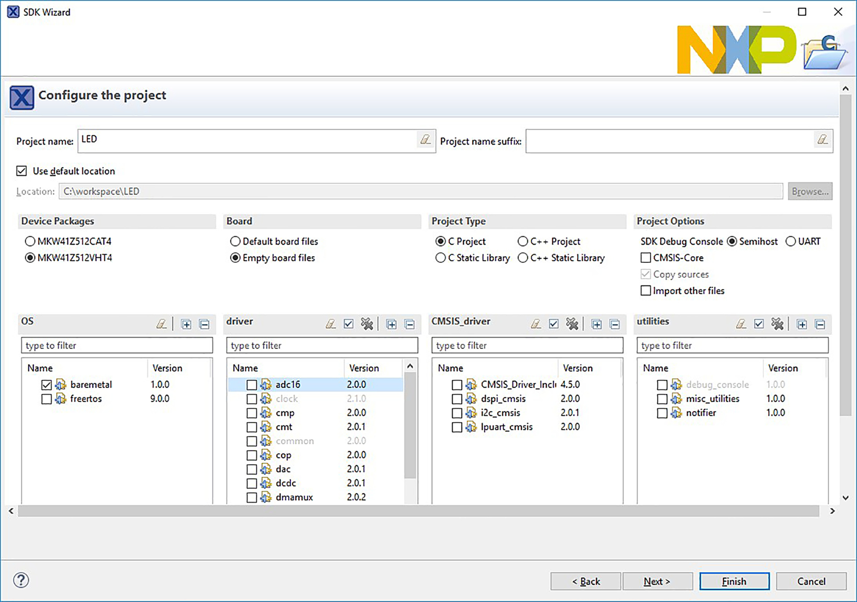
Fig. 11 Configuring a project for baremetal libraries only.
Continuing with the SDK Wizard:
- - Unselect “Redirect SDK ‘PRINTF’ to C Library ‘printf’.”
- - Unselect “Include semihost HardFault handler.”
- - Click Finish (Fig. 12).
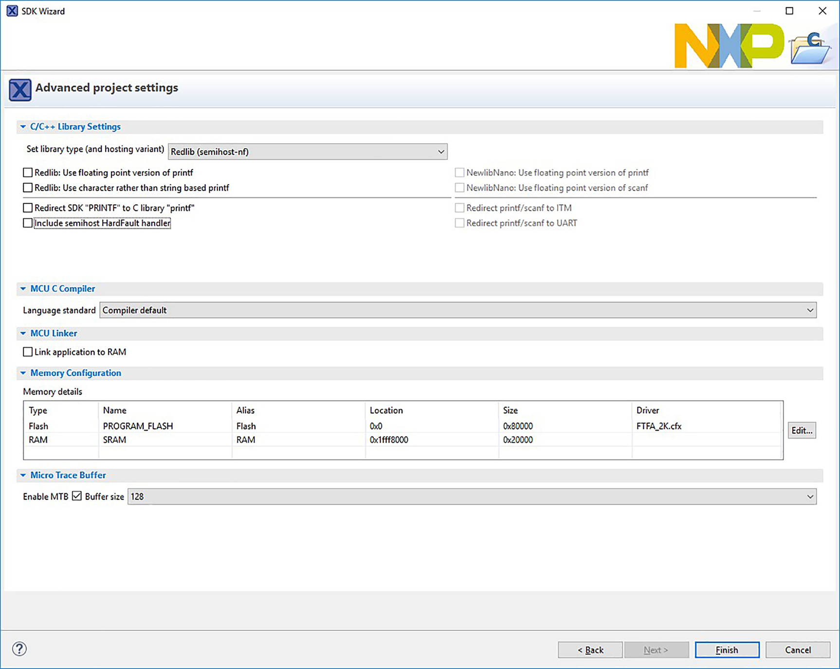
Fig. 12 Additional baremetal project setting.
In the project explorer, expand the project and source folder and open the source file containing main(). The filename will be the same as the project name and have a .c extension. Delete all the text in the file and replace it with the text included below:
- /* Bare metal example to blink the RED LED */
- int main(void) {
- unsigned int temp;
- volatile unsigned int i;
- /* Port C Clock Gate Control: Clock enabled */
- temp = *(unsigned int *)(0x40048038); /* Read System Clock Gating Control Register 5 (SIM_SCGC5) */
- temp |= 0x800; /* Enable clocking to PORTC */
- *(unsigned int *)(0x40048038) = temp; /* Write the new value to the control register */
- /* PORTC1 (pin 37) is configured as PTC1 */
- *(unsigned int *)(0x4004b004) = 0x105; /* Setup pin mux to make RED LED I/O an output */
- /* Init output LED GPIO. */
- *(unsigned int *)(0x400ff088) = 0x02; /* Write base + PCOR to turn off the RED LED */
- *(unsigned int *)(0x400ff094) = 0x02; /* Write base + PDDR to set the RED LED I/O pin to output */
- while (1)
- {
- /* Delay for a bit */
- for (i = 0; i < 800000; ++i)
- {
- __asm("NOP"); /* delay */
- }
- /* Toggle the RED LED I/O pin */
- *(unsigned int *)(0x400ff08c) = 0x02; /* Write base + PTOR to toggle output pin for RED LED */
- }
- return 0;
- }
Save the source file, then build the project by right-clicking on the project name in the Project Explorer and selecting Build Project. Monitor the build output in the console view. When finished, debug and run the program and observe the blinking LED action. To debug the program, follow the steps outlined in Section 5.3.
5.2 Basic Serial I/O—Polled UART Send/Receive
This example sends and receives characters using the serial port typically used to communicate using the RS-232 standard. Semiconductor vendors use various names for these devices, but the most common name is a UART (Universal Asynchronous Receiver Transmitter). In its simplest mode of operation, a UART will take an 8-bit byte (typically representing an ASCII character) and transmit each bit using the UART’s TX signal. It also receives individual bits on the UART’S RX signal and converts them to an 8-bit byte. Modern implementations of these devices support a wide variety of configuration options—bits per word, bit rate (BAUD), hardware flow control, etc. The device can be used in polled mode where the application polls the various status bits to determine when and how to access the UART registers. The device can be configured to run in an interrupt-driven mode where an interrupt is triggered when a certain condition is true. The features and programming modes of the UART are beyond the scope of this chapter. Details can be found in the programmer’s reference guide. For this example, the program initializes the configuration registers, then loops forever checking for input characters. When a character is received on the RX signal, that character is then transmitted out the TX signal.
The transmit and receive signals for UART0 can be found on the J1 header on the reference board. In its default configuration, the transmit signal, UART0_TX, is located on pin J1–2. The receive signal, UART0_RX, is located on pin J1–1. It is important to note that many reference boards are designed so the UART external I/O pins operate at “logic levels” and do not meet the RS-232 specification. These “logic level” UART signals are often referred to as “TTL level” signals. To meet the specification, additional hardware circuitry is needed to provide the required level shifting. This additional circuitry can take several forms. One way is to use an adapter board containing the required circuitry. When this type of board is used, it will typically contain the industry standard 9-pin D-style serial connector. Another way is to use a USB to TTL Serial cable. This type of cable contains a USB type-A connector on one end and several single pin connectors on the other. These single pin connectors are often called “flying leads.” The USB type-A end plugs into a host computer and appears as a USB Serial port to the host operating system. The individual pin connectors on the other end are then pressed onto the appropriate pins on the reference board. For our example, the cable pins labeled Tx, Rx, and GND should be connected to J1–1 (UART0_RX), J1–2 (UART0_TX), and J2–7 (GND).
If using an adapter cable, follow the vendor’s installation instructions, being sure to install any device drivers, if required. You can then use any terminal program to connect to the host’s serial port corresponding to the cable (i.e., COMx:). The serial port settings should be set to 115,200 baud, 8-bit word length, no parity, 1 stop bit.
For this example, we will use the sample driver program included in the SDK. Here are the steps to build the project:
- - Select File | New | Project…
- - Expand the MCUXpresso IDE group and select Import SDK Examples. Click Next (Fig. 13).
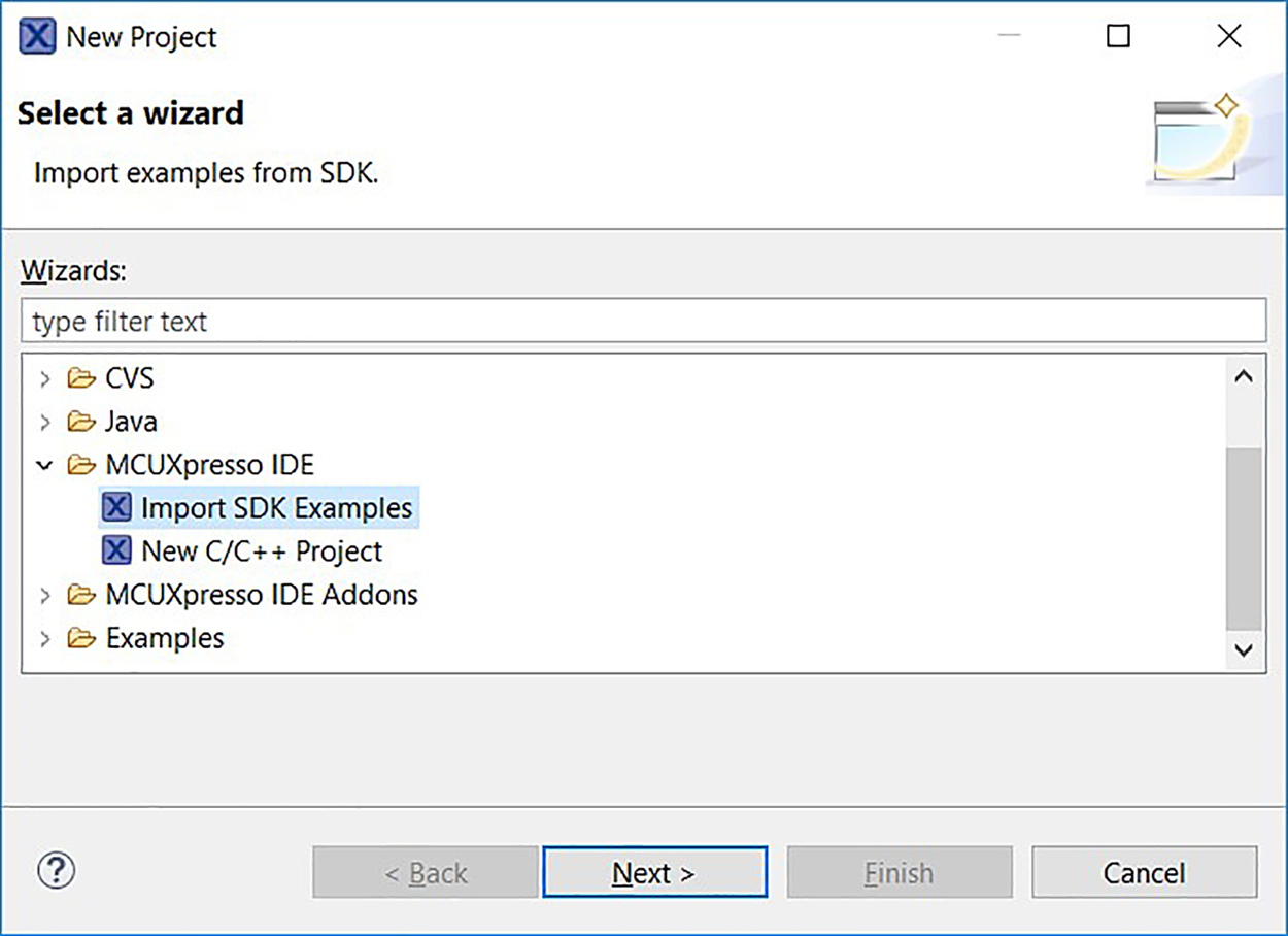
Fig. 13 Importing an SDK example project. - - Click on the frdmkw41z board, then click Next.
- - Expand the driver_examples group, expand the lpuart group, then check the box for polling. Click Finish (Fig. 14).

Fig. 14 Selecting the polled lpuart example. - - Build the project by right-clicking on the project name in the project explorer (frdmkw41z_driver_examples_lpuart_polling) and left-click on Build Project.
Expand the project in the project explorer, then expand the source group. The application can be found in lpuart_polling.c. This example uses the high-level library routines described earlier to initialize the system. The application is shown below. The routine BOARD_InitPins() configures the I/O pins, routine BOARD_BootClock_RUN() configures the clocks, and routine CLOCK_SetLpuartClock(0x1U) sets up the clocking needed for the UART. The program then configures the UART communications settings using the high-level structures and routines provided by the SDK. It initializes the configuration structure to a default set of values, then sets the desired baud rate and enables both transmit and receive functions in the structure. Calling LPUART_Init() uses the settings in the configuration structure to write the UART registers as required. At this point the UART is ready to transmit and receive data.
uint8_t txbuff[] = "Lpuart polling example
Board will send back received characters
";
int main(void)
{
uint8_t ch;
lpuart_config_t config;

BOARD_InitPins();
BOARD_BootClockRUN();
CLOCK_SetLpuartClock(0x1U);

/*
* config.baudRate_Bps = 115200U;
* config.parityMode = kLPUART_ParityDisabled;
* config.stopBitCount = kLPUART_OneStopBit;
* config.txFifoWatermark = 0;
* config.rxFifoWatermark = 0;
* config.enableTx = false;
* config.enableRx = false;
*/
LPUART_GetDefaultConfig(&config);
config.baudRate_Bps = BOARD_DEBUG_UART_BAUDRATE;
config.enableTx = true;
config.enableRx = true;

LPUART_Init(DEMO_LPUART, &config, DEMO_LPUART_CLK_FREQ);
Now that the UART is ready to use, the application transmits the string defined in txbuff[], then loops forever reading and echoing characters:
LPUART_WriteBlocking(DEMO_LPUART, txbuff, sizeof(txbuff) - 1);

while (1)
{
LPUART_ReadBlocking(DEMO_LPUART, &ch, 1);
LPUART_WriteBlocking(DEMO_LPUART, &ch, 1);
}
}
To debug the program, right-click on the project name, then select Debug As, then select SEGGER J-Link probes. The debugger will reset the target, download the program, and run the program to a temporary breakpoint placed at main(). Be sure your terminal program is running on the host PC and is configured properly. To run the example program, press the F8 function key. The string in txbuff[] will be displayed in the terminal window. Typed characters will be echoed back to the terminal. Note that the characters may be displayed twice if your terminal program has its “local echo” option enabled.
5.3 Overview of Interrupt Handlers
One of the peripherals most commonly used in embedded designs is the timer. Many of the larger, highly integrated SoCs will contain multiple types of timers, and often support different operating modes and capabilities. Some are designed as periodic interrupt timers (PIT) and can be used to generate interrupts at a constant rate, and others generate periodic waveforms (PWM) or time the rise and fall of input signals (input capture). Other types of timer models can function as counters, using internal or external signals as the event to be counted. On our reference board, the SoC provides three types of timers: a Timer/PWM Module (TPM), a Periodic Interrupt Timer (PIT), and a Low-Power Timer (LPTMR). For this example, we will use the LPTMR module to count the transitions of an internal clock source.
This example also illustrates the use of an interrupt. The LPTMR will be configured to count clock cycles and then generate an interrupt when enough clocks have been counted to equal one second. This will cause our interrupt handler to be called, toggling the LED and signaling that the time interval elapsed. This process will then repeat forever.
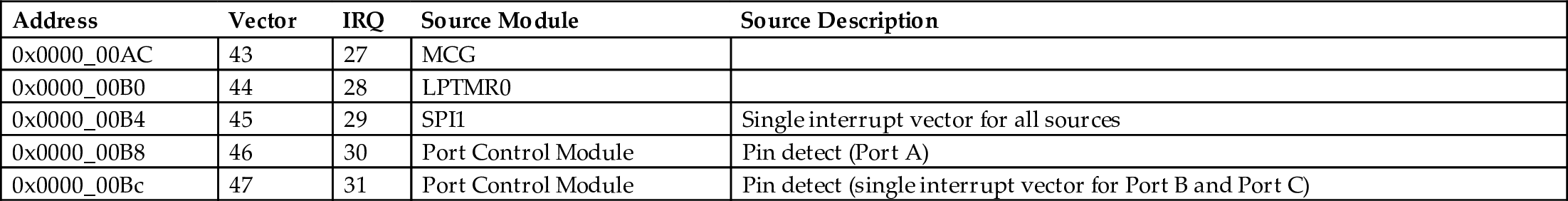
Before we go into the details of the example, we will provide some details on interrupts and how they are handled in this example. Using Table 3-6 in the KW41Z reference manual, we can see that the LPTMR module is assigned to interrupt (IRQ) number 28 (gray shading below) and it corresponds to vector number 44. See Table 2.
Table 2
| Address | Vector | IRQ | Source Module | Source Description |
|---|---|---|---|---|
| 0x0000_00AC | 43 | 27 | MCG | |
| 0x0000_00B0 | 44 | 28 | LPTMR0 | |
| 0x0000_00B4 | 45 | 29 | SPI1 | Single interrupt vector for all sources |
| 0x0000_00B8 | 46 | 30 | Port Control Module | Pin detect (Port A) |
| 0x0000_00Bc | 47 | 31 | Port Control Module | Pin detect (single interrupt vector for Port B and Port C) |
The startup code described earlier takes care of initializing the processor’s interrupt vector table. For the LPTMR, the entry can be found in startup_mkw41z4.c. Here are parts of the file that that apply to our example:
WEAK void LPTMR0_IRQHandler(void);
void LPTMR0_DriverIRQHandler(void) ALIAS(IntDefaultHandler);

MCG_IRQHandler,   // 43: MCG interrupt
LPTMR0_IRQHandler, // 44: LPTMR0 interrupt
SPI1_IRQHandler,   // 45: SPI1 single interrupt vector for all sources
PORTA_IRQHandler,  // 46: PORTA Pin detect
PORTB_PORTC_IRQHandler, // 47: PORTB and PORTC Pin detect

WEAK_AV void LPTMR0_IRQHandler(void)
{ LPTMR0_DriverIRQHandler();
}

WEAK_AV void IntDefaultHandler(void)
{ while(1) {}
}
Note the two functions listed in the code snippet, LPTMR0 and IntDefaultHandler, are defined using the WEAK designation. This is a feature that tells the compiler to use the locally-defined function, LPTMR0_IRQHandler(void), unless another definition of the function is encountered during the linking process. This allows a developer to define their own version of LPTMR0_IRQHandler(void) in their application and use it in the build process, with the one in the startup code being ignored.
It is also common to initialize all unused interrupt vectors to point to an infinite loop that does nothing. This allows the developer to “catch” unexpected interrupts. These are interrupts that may have been enabled in the peripheral control registers without first defining an interrupt service routine to handle the interrupt. The startup code does this by defining all the interrupt handlers to be IntDefaultHandler(). This function only contains a while(1) {} statement. Using a debugger, the developer can halt the processor. If it is executing this infinite loop, it tells the developer an unassigned interrupt occurred, and the system and peripheral registers can be examined to determine the cause.
5.4 Basic Timer Operation—Low-Power Timer (LPTMR)
For this example, we will use the sample driver program included in the SDK. Here are the steps to build the project:
- - Select File | New | Project…
- - Expand the MCUXpresso IDE group and select Import SDK Examples. Click Next (Fig. 15).

Fig. 15 Importing an SDK example project. - - Click on the frdmkw41z board, then click Next.
- - Expand the driver_examples group, then check the box for lptmr. Click Finish (Fig. 16).
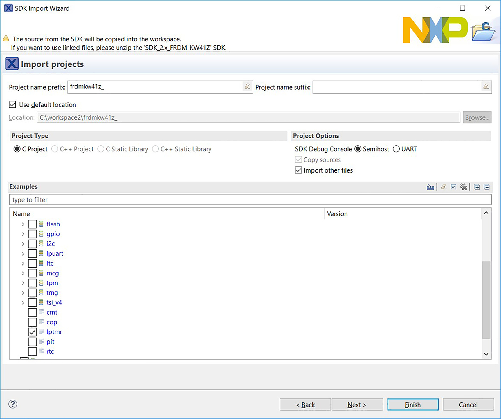
Fig. 16 Selecting the polled lptimer example. - - Build the project by right-clicking on the project name in the project explorer (frdmkw41z_driver_examples_lptmr) and left-click on Build Project.
Expand the project in the project explorer, then expand the source group. The application can be found in lptmr.c. This example uses the high-level definitions described earlier and defines the interrupt handler needed for the timer. This is the interrupt handler routine:
#define LPTMR_LED_HANDLER LPTMR0_IRQHandler
volatile uint32_t lptmrCounter = 0U;

void LPTMR_LED_HANDLER(void)
{
LPTMR_ClearStatusFlags(LPTMR0, kLPTMR_TimerCompareFlag);
lptmrCounter ++;
LED_TOGGLE();
/*
* Workaround for TWR-KV58: because write buffer is enabled, adding
* memory barrier instructions to make sure clearing interrupt flag completed
* before go out ISR
*/
__DSB();
__ISB();
}
The interrupt handler routine performs three operations:
- - Resets the LPTMR status. This clears the interrupt signal the LPTMR module uses internally to alert the processor. The module is then ready to interrupt the next time the count reaches 1 s.
- - Increments the variable shared between the interrupt handler (LPTMR_LED_HANDLER) and the main application. Note that this variable, lptmrCounter, is defined using the keyword “volatile.” This keyword prevents the compiler from removing the code that accesses the variable when optimization is turned on. After this variable is initialized to zero in main(), it is only read repeatedly. The keyword tells the compiler that the variable is being written in another context and that it should be handled as if it may change value over time.
- - Toggles the LED.
As mentioned earlier, the LPTMR0_IRQHandler is defined in the startup code as WEAK. This means the address in the interrupt vector table corresponding to vector 44 will be replaced with the address of the new interrupt handler from the example application. When the LPTMR interrupt occurs, the processor will fetch the address from the vector table (for vector 44) and jump to that location, LPTMR_LED_HANDLER in the example application.
The main application is shown below. The routine BOARD_InitPins() configures the I/O pins, routine BOARD_BootClock_RUN() configures the clocks, and routine BOARD_InitDebugConsole() sets up a debug console to redirect PRINTF() statements through a virtual UART contained in the JTAG debugger connection. This debug console allows the developer to add a console connection without using the LPUART peripheral and a physical serial cable connection. The program then configures the LPTMR settings using the high-level structures and routines provided by the SDK. It initializes the configuration structure (lptmrConfig) to a default set of values, then writes these values to the timer by calling LPTMR_Init(). The function LPTMR_SetTimerPeriod() sets the timeout interval to 1 s.
At this point in the code, the timer has been configured as required in the example. The two remaining steps are to enable the timer interrupt and to tell the timer to start counting. LPTMR_EnableInterrupts() enables the interrupt in the LPTMR module and EnableIRQ() enables the LPTMR interrupt in the processor. To tell the module to start counting, LPTMR_StartTimer() is called.
The application then goes into a loop, checking to see if the variable shared with the interrupt handler, lptmrCounter, has changed. If so, it saves a copy of the counter and prints a message on the console.
int main(void)
{
uint32_t currentCounter = 0U;
lptmr_config_t lptmrConfig;

LED_INIT();

/* Board pin, clock, debug console init */
BOARD_InitPins();
BOARD_BootClockRUN();
BOARD_InitDebugConsole();

/* Configure LPTMR */
/*
* lptmrConfig.timerMode = kLPTMR_TimerModeTimeCounter;
* lptmrConfig.pinSelect = kLPTMR_PinSelectInput_0;
* lptmrConfig.pinPolarity = kLPTMR_PinPolarityActiveHigh;
* lptmrConfig.enableFreeRunning = false;
* lptmrConfig.bypassPrescaler = true;
* lptmrConfig.prescalerClockSource = kLPTMR_PrescalerClock_1;
* lptmrConfig.value = kLPTMR_Prescale_Glitch_0;
*/
LPTMR_GetDefaultConfig(&lptmrConfig);

/* Initialize the LPTMR */
LPTMR_Init(LPTMR0, &lptmrConfig);

/*
* Set timer period.
* Note : the parameter "ticks" of LPTMR_SetTimerPeriod should be equal or greater than 1.
*/
LPTMR_SetTimerPeriod(LPTMR0, USEC_TO_COUNT(LPTMR_USEC_COUNT, LPTMR_SOURCE_CLOCK));

/* Enable timer interrupt */
LPTMR_EnableInterrupts(LPTMR0, kLPTMR_TimerInterruptEnable);

/* Enable at the NVIC */
EnableIRQ(LPTMR0_IRQn);

PRINTF("Low Power Timer Example
");

/* Start counting */
LPTMR_StartTimer(LPTMR0);
while (1)
{
if (currentCounter != lptmrCounter)
{
currentCounter = lptmrCounter;
PRINTF("LPTMR interrupt No.%d
", currentCounter);
}
}
}
To debug the program, right-click on the project name, then select Debug As, then select SEGGER J-Link probes. The debugger will reset the target, download the program, and run the program to a temporary breakpoint placed at main(). Be sure the console tab is selected so the characters printed in the debug console are visible. To run the program, press the F8 function key. The output will appear in the console:
SEGGER J-Link GDB Server V6.32h - Terminal output channel
Low Power Timer Example
LPTMR interrupt No.1
LPTMR interrupt No.2
LPTMR interrupt No.3
Placing a breakpoint in the interrupt handler allows the developer to verify the interrupt is being generated and their handler is being called.
6 Summary
Using a low-cost reference board with the manufacturer’s SDK allows a developer to quickly ramp up on low-level, embedded development. Understanding how to use the peripherals covered in this chapter provides a foundation to build small, basic embedded applications. Once a base platform is created, the developer can easily leverage more advanced features of the SoC and SDK and add support for wireless communications, displays, and storage devices.
Questions and Answers
- 1. List some of the mechanisms used to configure modern SoCs at reset. Provide configuration examples typically controlled by these settings.
- a. Mechanisms. Pull-up resistors on I/O or bus signals, configuration word in flash.
- b. Examples of settings. Pin direction (input vs. output), enable internal pull-up resistor, interrupt enable, edge vs. level activation.
- 2. What are some of the “behind the scenes” initialization steps the SDK boot code performs prior to calling main()?
- a. Disable the watchdog timer.
- b. Initialize the .data sections in RAM.
- c. Initialize the .bss section in RAM to all zeros.
- 3. List three types of timers on the SoC used in this chapter and give an example of a function each can perform.
- a. Periodic Interrupt Timer (PIT)—generates repetitive interrupts at a fixed interval that can be used to trigger interrupts at a constant rate.
- b. Timer/PWM module (TPM)—can be used to generate periodic waveforms.
- c. Low-power Timer module (LPTMR)—used to count internal or external signals.
- 4. Give an example of a use case where the Processor ID register might be used.
- a. When the errata documentation indicates different software behavior is needed based on the silicon revision of the SoC.