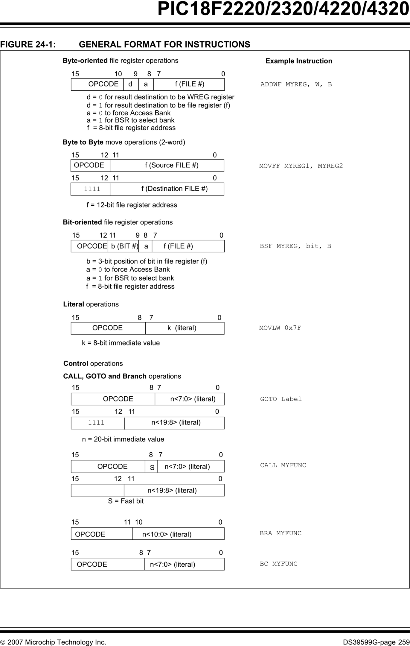
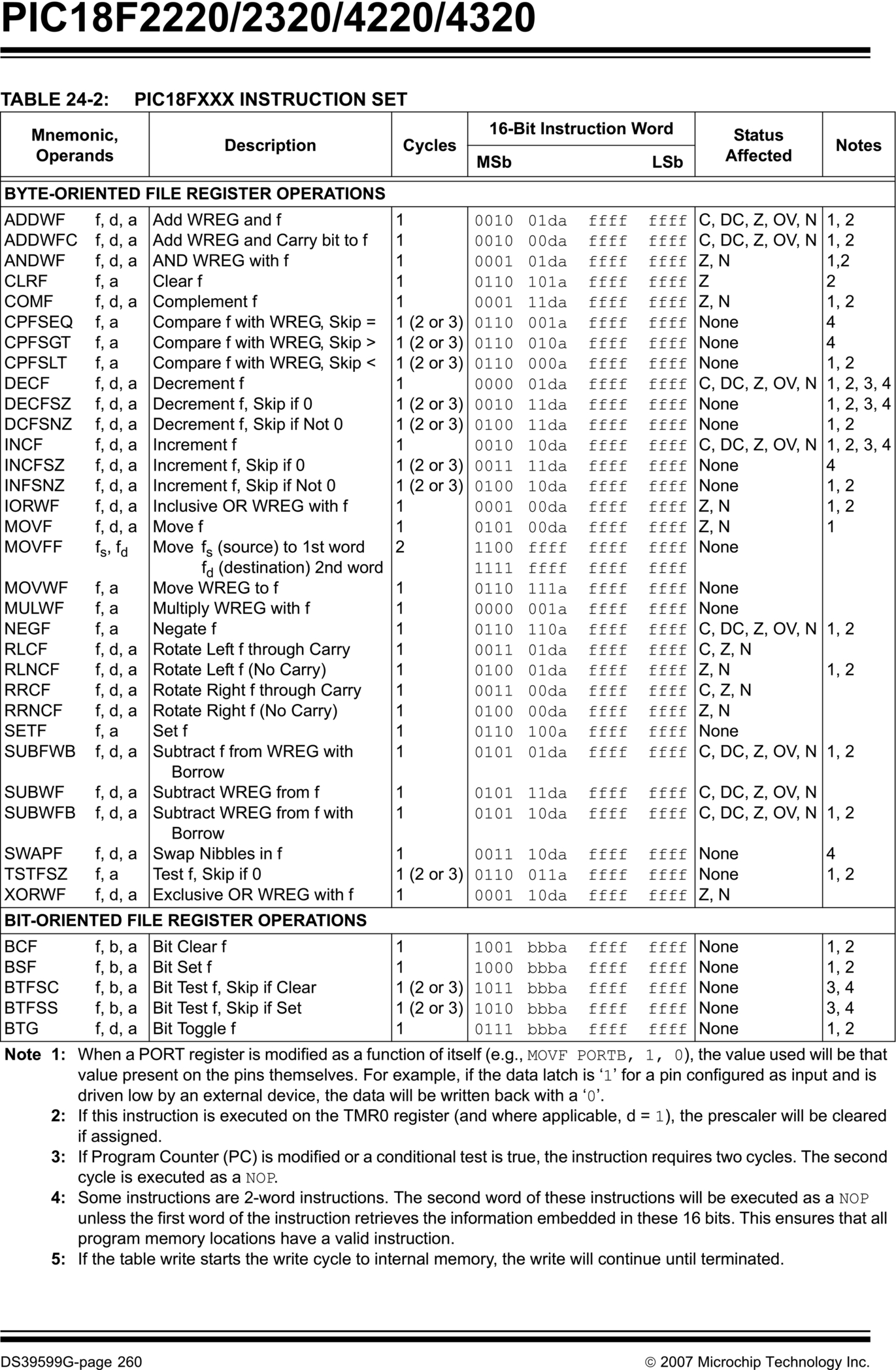
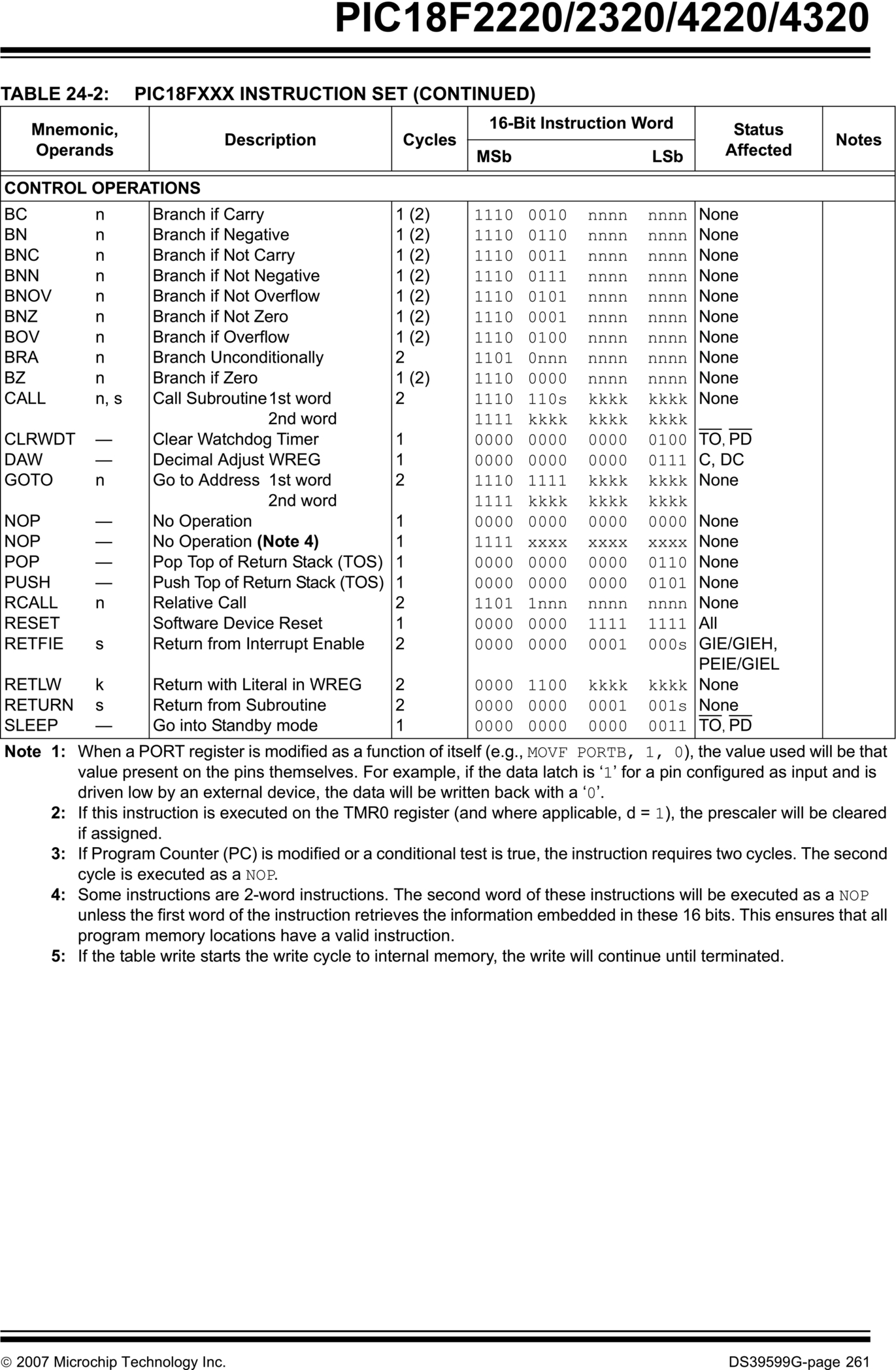
Instruction Sets
- Baseline PIC 174–175
- Comparison Table 176–177
- 10F2xx 178–180
- 12F519 181–183
- 16F6xx 184–186
- 18Fxxxx 187–193
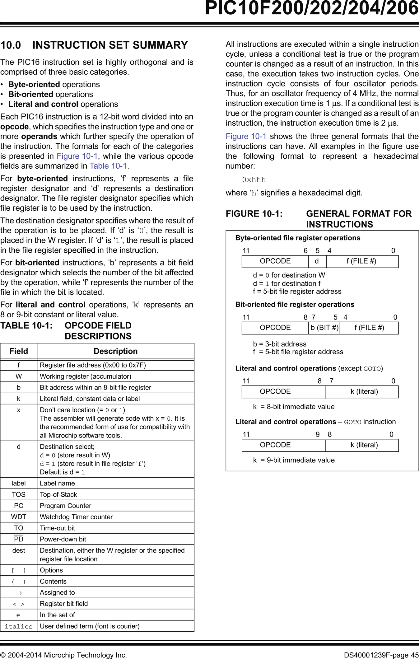
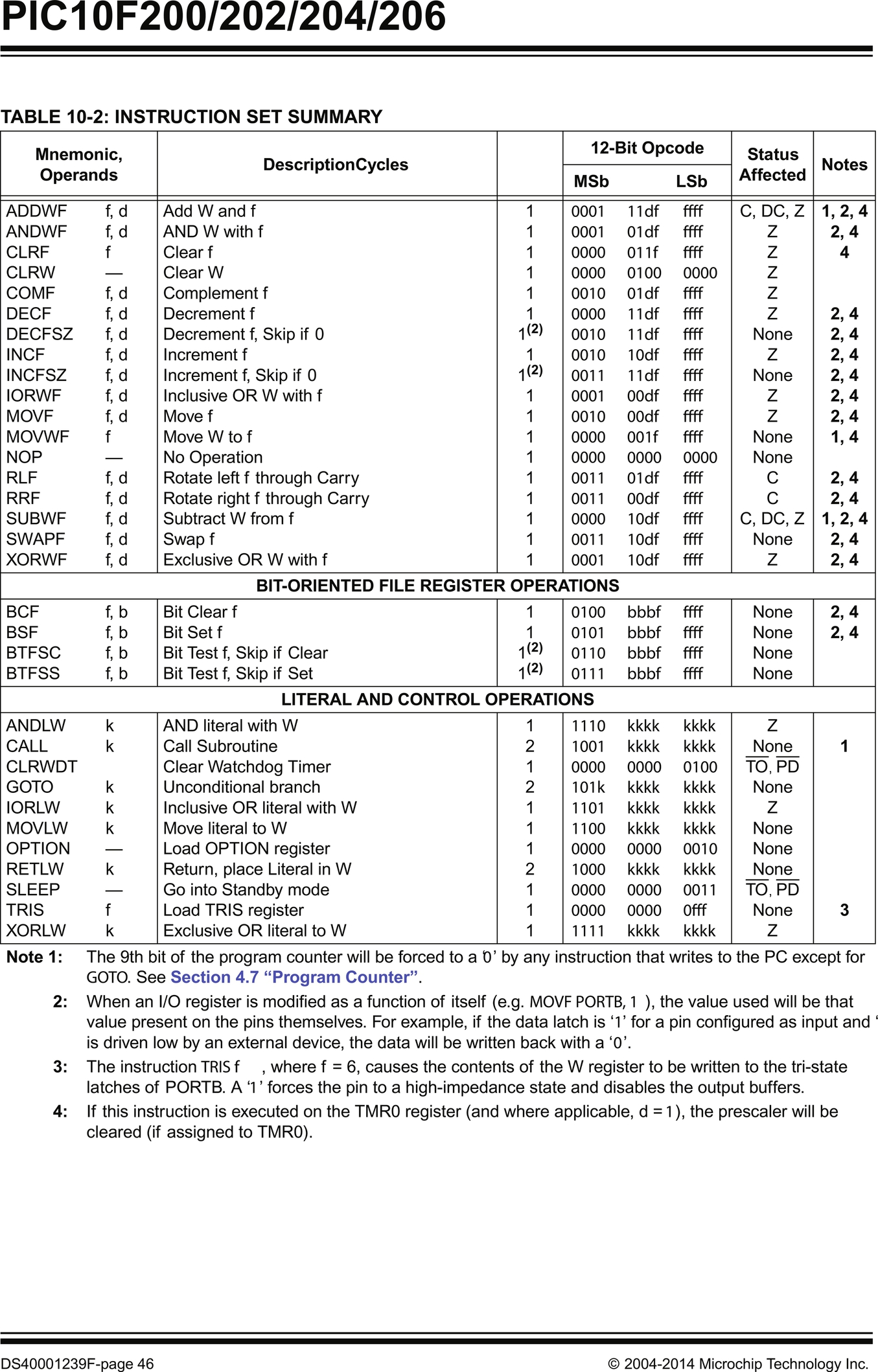
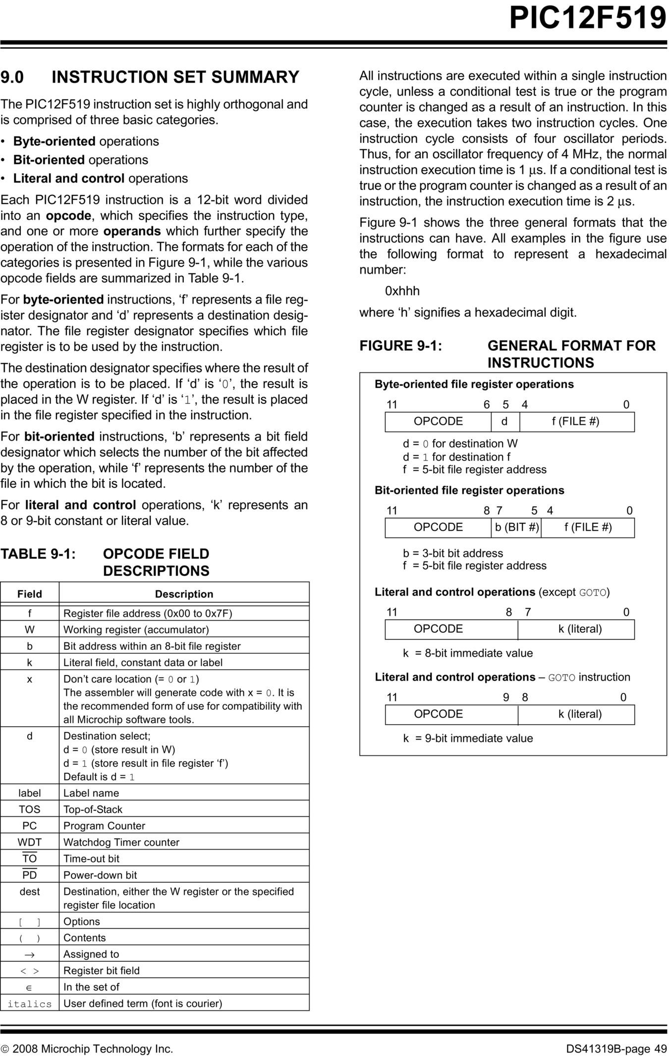
Baseline PIC MCU Instruction Set
This applies to the PIC10F2xx, PIC12C5xx, PIC12F5xx, PIC16C5xx, and PIC16F5xx families.
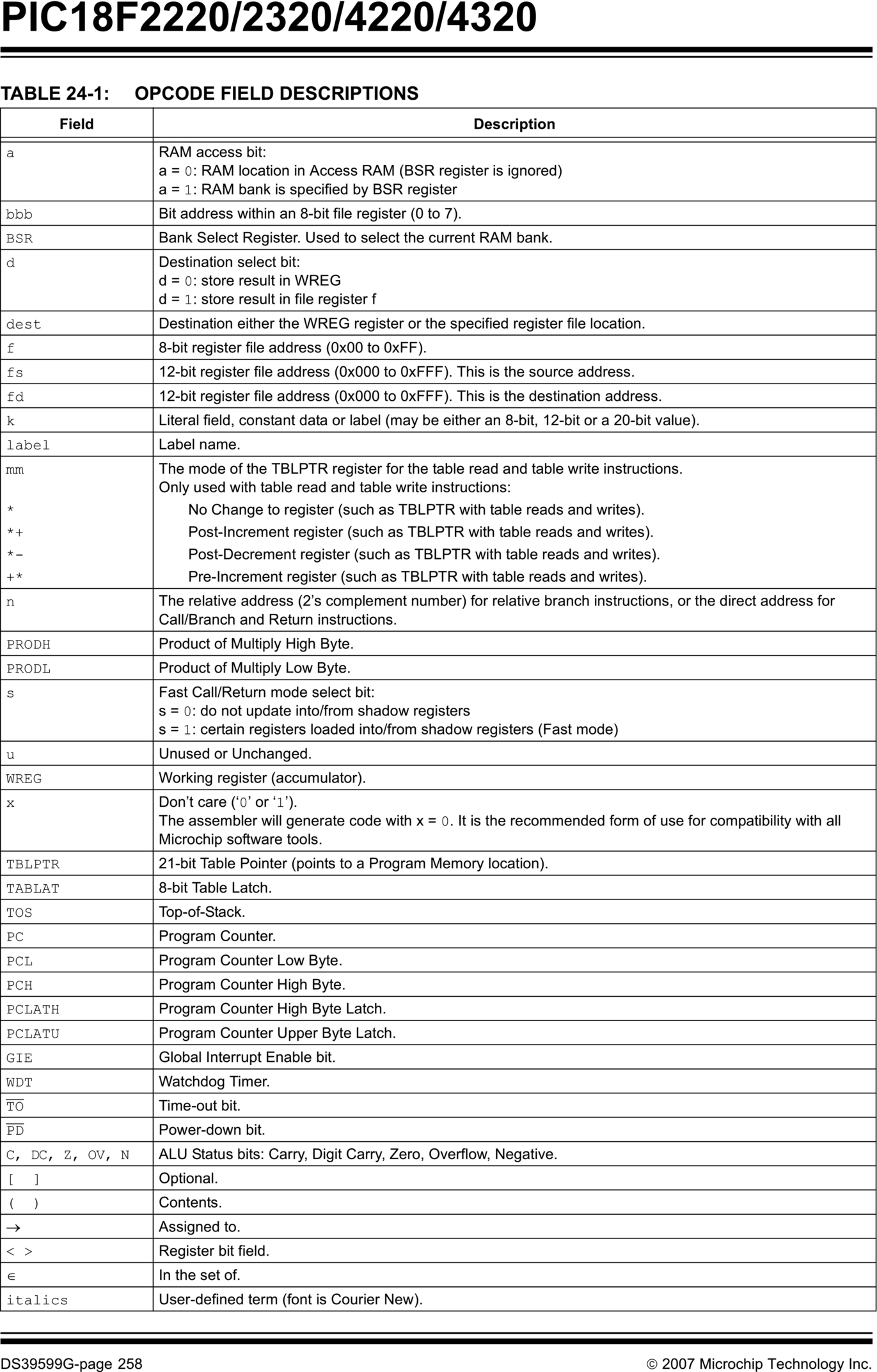
| Mneumonic | Operands | Description | Cycles | 12-Bit Opcode (MSB…LSB) | Status Affected | Notes |
|---|---|---|---|---|---|---|
| Byte-oriented operations | ||||||
| ADDWF | f,d | ADD W with f | 0001 11df ffff | C,DC,Z | 1,2,4 | |
| ANDWF | f,d | AND W with f | 1 | 0001 01df ffff | Z | 2,4 |
| CLRF | f | Clear f | 1 | 0000 011f ffff | Z | 4 |
| CLRW | Clear W | 1 | 0000 0100 0000 | Z | ||
| COMF | f,d | Complement f | 1 | 0010 01df ffff | Z | |
| DECF | f,d | Decrement f | 1 | 0000 11df ffff | Z | 2,4 |
| DECFSZ | f,d | Decrement f, Skip if 0 | 1(2) | 0010 11df ffff | None | 2,4 |
| INCF | f,d | Increment f | 1 | 0010 10df ffff | Z | 2,4 |
| INCFSZ | f,d | Increment f, Skip if 0 | 1(2) | 0011 11df ffff | None | 2,4 |
| IORWF | f,d | Inclusive OR W with f | 1 | 0001 00df ffff | Z | 2,4 |
| MOVF | f,d | Move f | 1 | 0010 00df ffff | Z | 2,4 |
| MOVWF | f | Move W to f | 1 | 0000 001f ffff | None | 1,4 |
| NOP | No Operation | 1 | 0000 0000 0000 | None | ||
| RLF | f,d | Rotate left f through Carry | 1 | 0011 01df ffff | C | 2,4 |
| RRF | f,d | Rotate right f through Carry | 1 | 0011 00df ffff | C | 2,4 |
| SUBWF | f,d | Subtract W from f | 1 | 0000 10df ffff | C,DC,Z | 1,2,4 |
| SWAPF | f,d | Swap f | 1 | 0011 10df ffff | None | 2,4 |
| XORWF | f,d | Exclusive OR W with f | 1 | 0001 10df ffff | Z | 2,4 |
| Bit-oriented operations | ||||||
| BCF | f,b | Bit Clear f | 1 | 0100 bbbf ffff | None | 2,4 |
| BSF | f,b | Bit Set f | 1 | 0101 bbbf ffff | None | 2,4 |
| BTFSC | f,b | Bit Test f, Skip if Clear | 1(2) | 0110 bbbf ffff | None | |
| BTFSS | f,b | Bit Test f, Skip if Set | 1(2) | 0111 bbbf ffff | None | |
| Literal and control operations | ||||||
| ANDLW | k | AND literal with W | 1 | 1110 kkkk kkkk | Z | |
| CALL | k | Subroutine Call | 2 | 1001 kkkk kkkk | None | 1 |
| CLRWDT | Clear Watchdog Timer | 1 | 0000 0000 0100 | TO,PD | ||
| GOTO | k | Unconditional Branch | 2 | 101k kkkk kkkk | None | |
| IORLW | k | Inclusive OR literal with W | 1 | 1101 kkkk kkkk | Z | |
| MOVLW | k | Move literal to W | 1 | 1100 kkkk kkkk | None | |
| OPTION | Load OPTION register | 1 | 0000 0000 0010 | None | ||
| RETLW | k | Return, place literal in W | 2 | 1000 kkkk kkkk | None | |
| SLEEP | Go into standby mode | 1 | 0000 0000 0011 | TO, PD | ||
| TRIS | f | Load TRIS register | 1 | 0000 0000 0fff | None | 3 |
| XORLW | k | Exclusive OR literal with W | 1 | 1111 kkkk kkkk | Z | |
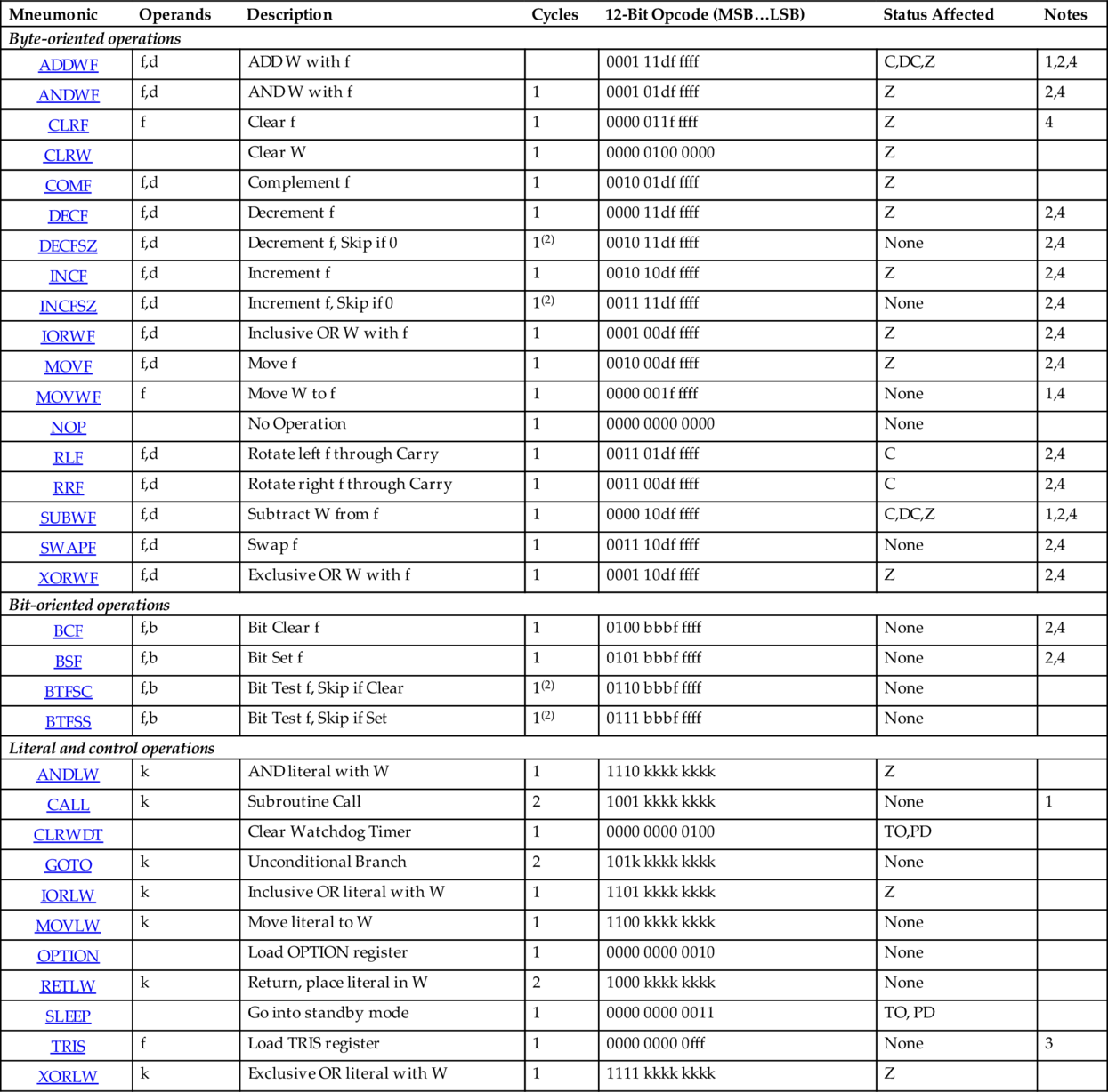
- 1. The ninth bit of the program counter will be forced to a “0” by any instruction that writes to the PC except for GOTO (see Section 3.5 “Program Counter” for more on program counter).
- 2. When an I/O register is modified, as a function of itself (e.g., MOVF PORTB, 1), the value used will be that value present on the pins themselves. For example, if the data latch is “1” for a pin configured as input and is driven low by an external device, the data will be written back with a “0.”
- 3. The instruction TRIS f, where f = 5, 6, or 7 causes the contents of the W register to be written to the tristate latches of PORTA, B or C, respectively.
- 4. A “1” forces the pin to a high impedance state and disables the output buffers.
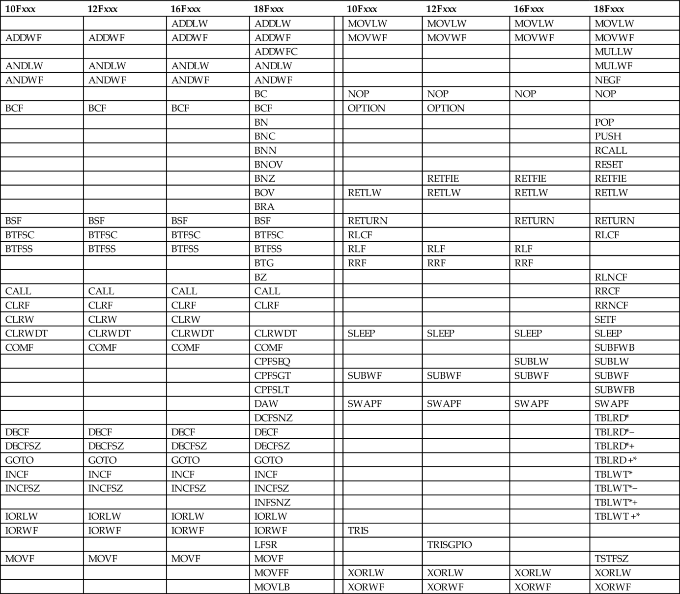
Comparison Table
| 10Fxxx | 12Fxxx | 16Fxxx | 18Fxxx | 10Fxxx | 12Fxxx | 16Fxxx | 18Fxxx | |
|---|---|---|---|---|---|---|---|---|
| ADDLW | ADDLW | MOVLW | MOVLW | MOVLW | MOVLW | |||
| ADDWF | ADDWF | ADDWF | ADDWF | MOVWF | MOVWF | MOVWF | MOVWF | |
| ADDWFC | MULLW | |||||||
| ANDLW | ANDLW | ANDLW | ANDLW | MULWF | ||||
| ANDWF | ANDWF | ANDWF | ANDWF | NEGF | ||||
| BC | NOP | NOP | NOP | NOP | ||||
| BCF | BCF | BCF | BCF | OPTION | OPTION | |||
| BN | POP | |||||||
| BNC | PUSH | |||||||
| BNN | RCALL | |||||||
| BNOV | RESET | |||||||
| BNZ | RETFIE | RETFIE | RETFIE | |||||
| BOV | RETLW | RETLW | RETLW | RETLW | ||||
| BRA | ||||||||
| BSF | BSF | BSF | BSF | RETURN | RETURN | RETURN | ||
| BTFSC | BTFSC | BTFSC | BTFSC | RLCF | RLCF | |||
| BTFSS | BTFSS | BTFSS | BTFSS | RLF | RLF | RLF | ||
| BTG | RRF | RRF | RRF | |||||
| BZ | RLNCF | |||||||
| CALL | CALL | CALL | CALL | RRCF | ||||
| CLRF | CLRF | CLRF | CLRF | RRNCF | ||||
| CLRW | CLRW | CLRW | SETF | |||||
| CLRWDT | CLRWDT | CLRWDT | CLRWDT | SLEEP | SLEEP | SLEEP | SLEEP | |
| COMF | COMF | COMF | COMF | SUBFWB | ||||
| CPFSEQ | SUBLW | SUBLW | ||||||
| CPFSGT | SUBWF | SUBWF | SUBWF | SUBWF | ||||
| CPFSLT | SUBWFB | |||||||
| DAW | SWAPF | SWAPF | SWAPF | SWAPF | ||||
| DCFSNZ | TBLRD* | |||||||
| DECF | DECF | DECF | DECF | TBLRD*− | ||||
| DECFSZ | DECFSZ | DECFSZ | DECFSZ | TBLRD*+ | ||||
| GOTO | GOTO | GOTO | GOTO | TBLRD +* | ||||
| INCF | INCF | INCF | INCF | TBLWT* | ||||
| INCFSZ | INCFSZ | INCFSZ | INCFSZ | TBLWT*− | ||||
| INFSNZ | TBLWT*+ | |||||||
| IORLW | IORLW | IORLW | IORLW | TBLWT +* | ||||
| IORWF | IORWF | IORWF | IORWF | TRIS | ||||
| LFSR | TRISGPIO | |||||||
| MOVF | MOVF | MOVF | MOVF | TSTFSZ | ||||
| MOVFF | XORLW | XORLW | XORLW | XORLW | ||||
| MOVLB | XORWF | XORWF | XORWF | XORWF |


..................Content has been hidden....................
You can't read the all page of ebook, please click here login for view all page.