Introduction
Keywords
Pseudocode; Algorithm; Program; Development; Core family; Practical; Data sheet; Embedded control; Assembly; Implementation
Practical Applications
Common applications for embedded control are devices or systems that require simple repeatable programs, with limited interaction from the user, such as switch inputs or light emitting diodes (LED) outputs. Generally, once programmed, the device continues to operate for years without any necessary changes, unless there is a desire to change the performance. The most common occurrence requiring rewriting of the program is, generally, the need to add features or performance improvements in coming years. In this text, the conscientious design of the microcontroller program is laid out in a manner to maintain upward compatibility. If you follow through with using this approach in your own designs, it will pay back in the future.
Some practical applications, suggested by Microchip, include:
- • Identification tags
- • Drug tester
- • Electronic lock
- • Electronic chime
- • Pressure sensor
- • Water consumption gauge
- • Medication dispenser
- • LED flashlight
- • Intelligent power switch
- • Light dimmer
- • Fan controller
- • Smoke/CO alarm
- • Engine governor
- • Protocol handler
- • Flat iron temperature control
- • Capacitive switch
- • Irrigation controller
- • Security monitor
Beginning with the use of Sets and operators (such as op, opcode, or operation) the relationship between real-world applications and program representation is introduced. The set S is a relationship between a set S and itself, where x ρ y is a relation “on S” that represents x and y.
Our program example will show how the elements, coins, and pushbuttons are part of a vending machine program. In this example, x is a coin which will be received prior to the selection pushbutton. They could represent a list of coins that are acceptable. Then y is a list of pushbuttons that may be selected.
Why Assembly?
There are numerous reasons to program in Assembly Language. Generally, Assembly Language is simply more efficient. One of two explanations will be appropriate: the code will take less time to execute and it will take less memory space to execute.
- From Jan Hext, in his book Programming Structures, an example of simply accessing memory to illustrate how assembly code can use registers to accomplish the task of interchanging the values of A and B. With a high level language, an additional memory location will be necessitated. A total of six memory accesses is required.
- temp := A ; Memory-to-memory requires 2 accesses
- A := B; Memory-to-memory requires 2 accesses
- B := temp ; Memory-to-memory requires 2 accesses
- With Assembly Language, registers are used which are much faster and do not require a memory access. A total of four memory accesses is required.
- R ← A ; Memory-to-register requires 1 access
- A ← B ; Memory-to-memory requires 2 accesses
- B ← R ; Register-to-memory requires 1 access
- This code may seem only minimally better than the high level language version. However, four (4) accesses versus six (6) is a savings of 33%. Some compilers do optimize and use registers. However, this is not always the case.
In addition, when some form of a loop structure is used, the net effect is to multiply the number of accesses by the number of control loops. This is where it will clearly show an unhelpful multiplication effect. For example, if the loop was “FOR T = 1 to 10, NEXT,” the total accesses on the high level language side would be 60 (plus 10 for the loop counter) compared with the assembly language approach of 40 (plus 0 for the loop counter executed with the use of a register.) This would result in a savings of (70–40)/70 or approximately 43%.
Core Families (“Baseline,” “Midrange,” “Enhanced Midrange,” “High Performance”)
This text is intended to give the reader thorough information on using Microchip’s 8-bit Core Family Systems. Microchip groups their 8-bit products into three families: Baseline, Midrange, and Midrange Enhanced. These family systems have similar architecture, peripherals, and programming. Embedded control devices, or controllers, differ from processors as the controller user is not concerned, nor aware, with the use of devices to communicate with the controller. For example, the processor will have a keyboard and a monitor through which the user will communicate with the processor. In embedded control, the user will typically interface with the controller by way of switches and LEDs. The controller user will not necessarily even be aware of the controller’s clock speed, instruction cycles, and the like.
Baseline
Baseline families include the PIC10F, PIC12X5, PIC16X5X. The Baseline products have an 8-bit data memory access and a 12-bit wide instruction set. Paging is used to access four banks of program memory. These products have the smallest footprint of all products. There is even a small 6-pin SOT-23 in the 10F2xx series along with the 8-pin PDIP and 8-pin DFN. Low voltage operation, down to 2V, is available in the PIC16C5x and PIC10F2xx series. Features of the smallest PIC10F2xx include 33 single-word instructions; two-level deep stack; direct, indirect, and relative addressing modes for data and instructions; 8-bit wide data path; eight special function hardware registers; and an operating speed of 4 MHz, or 1 μs instruction cycle, generated by an internal clock.
Peripheral features include four input/output (I/O) pins: three with individual direction control and one input-only pin. Another feature is an 8-bit Real-Time clock/counter (TMR0) with 8-bit programmable prescalar and one comparator (on the PIC10F204/206 version) with an internal absolute voltage reference.
Mark McComb, a Technical Training Engineer, presented in his Webinar, the following summary of Baseline products. “Our 8-bit MCUs, including the PIC10, PIC12, PIC16, and PIC18 families, offer the designer a range of choices with variations in performance, memory and pin count. Baseline Products offer a 12-bit instruction set covering 6-40-Pins and up to 3 kByte program memory or 2k instructions with a basic peripheral set including comparators and Analog-to-Digital Converters.”
Midrange
Mark McComb further elaborates upon Microchip’s “existing Midrange family offers a 14-bit instruction set covering 8-64-Pins with up to 14 kByte program memory or 8k instructions. With up to 5 MIPS performance, a more advanced peripheral set is offered including Serial Communications, Capture/Compare/PWM, LCD, EEPROM, 10-bit A/D and, more recently, our Capacitive mTouch Sensing peripherals.”
McComb comments: “Recognizing the demand for increased performance and peripherals within the 8-bit MCU market, Microchip has recently revisited and enhanced the Midrange Architecture.”
Enhanced Midrange
“The new enhanced core builds upon the best elements of the existing Midrange core and provides additional performance, while maintaining compatibility with existing Midrange products for true product migration. The enhancements provide users with a boost of performance of up to 50% and code-size reductions of up to 40% for various algorithms and functions. Improvements such as more program and data memory including “C” efficiency optimizations, increased peripheral support, and reduced interrupt latency.
“Customers now have more options for applications that may not require the extended 16-bit program memory sizes offered by the PIC18 family but could benefit from more capabilities than currently offered by the existing Midrange architecture,” states McComb.
High Performance
“Finally, McComb states that the high-performance PIC18 products offer a 16-bit instruction set covering 18-100-Pins with up to 128 kByte program memory and up to 16 Million Instructions Per Second (MIPS) performance with hardware multiply. This family offers a very advanced peripheral set including Advanced Serial Communications (CAN, USB), Capture/Compare/PWM, LCD, USB, Ethernet, 12-bit A/D and the new Charge Time Measurement Peripheral developed specifically for capacitive sensing applications.” The high performance devices are beyond the scope of this text.
Data Sheet—Walk Through
Herein, we will take a look through the incorporated PIC10F200/202/204/206 data sheet from Appendix E. Follow along in Appendix E as we seek out information from the data sheet. Note that “reading” a data sheet is a little different from “reading” a book. In a typical book or novel, one generally starts at the beginning and reads each page to the last page. Technical data sheets are all about knowing how to seek out the information you need at any given time. It is important that you know how to look through the data sheet for the item(s) that you need. This means that it is also equally important to know how to ignore the information that you do not need. One does not read from beginning to end but rather scans for the required information within the datasheet format, generally, common among processors from one manufacturer.
Let’s explore this together. Let us presume that, today, we are looking for information on how to wire in inputs for a comparator. We are getting a printed circuit board laid out for use in our new project, before we start programming. As we gather information for our new project, pertinent information is highlighted in bold type.
What does the table of contents (TOC) show us? The TOC is found on page 3. First, however, we are getting a bit ahead of ourselves. Before we look at the TOC, we “backup” a little to first look at the summary page.
Glance through page 1 as this is a summary page. Page 1 shows a lot of information that you may need for quick reference. There is a lot of information, also, that does not help us with this specific issue. We find some information on the lower right side. It tells us that the one comparator uses an internal voltage reference and that both comparator inputs, as well as the output, are all visible externally. This is good information. This is found under “Peripheral Features” (PIC10F204/206.) We note that we must use either the 204 or the 206 version of the 10F to have access to the comparator.
After the summary page, the pinouts for the device are shown on page 2. Let’s look through each of the options. After perusing the pin labels, we know that we can use the 10F chip in any of the three packages: 6-pin SOT23, 8-pin PDIP, and 8-pin DFN. For ease of testing a prototype circuit board, we select the 8-pin PDIP as we can place a socket in this location and easily change processors if we damage it during testing.
Finally, we are at the TOC. Looking through it, we should peruse the General Description and the Device Varieties to ensure that we do not miss something of fundamental importance. Specifically, we need to understand information from the I/O Port generally, on page 20, and the Comparator Module, on page 31. We find, in the general description page, that there is a Table 1-1 that shows a comparison between the different versions of the chip. For the comparator, we know we cannot use the 200/202 version. We must use 204/206, as these are the only ones with the comparator. Looking at the Table, we note that the primary difference, between 204 and 206, is the Flash Program Memory and the Data Memory. As the pinouts are the same, we will note this information but not set our selection in stone as we have yet to write the software. Until the software has progressed, we really do not know whether we can use the 204 or need to step up to a 206.
Now, follow along as we move on to the I/O Port general information on page 20. We scan through this page. To scan, instead of “read,” look at the subtitles and the first sentence of each paragraph. This approach will allow you to select which paragraphs are relevant to our information search.
At Section 5.0, I/O PORT, we learn that upon Reset, all I/O ports are defined as inputs. We must ensure that we redefine the registers, immediately after reset, to guarantee that the pins are set as the comparator option. At Section 5.1, General Purpose Input/Output (GPIO), notes that the GPIO register low order bits of 0 through 3 are the only bits used. At Section 5.2, Tri-State (TRIS) Registers, we learn that additional registers are used to configure the GPIO pins and that GP3 is always configured as an input only. At Table 5-1, we note that the priority order of our comparator inputs is top priority 1. The priority order of the COUT on GP2 is 2, after the “oscillator divide by 4.” All other information on this page is more specific to software and registers and not needed at this time. This concludes our review of page 20.
Next, scanning the TOC, we move to page 31 Section 8.0, Comparator Module. This is the most important section for use of the Comparator Module. Scan the page, and the following pages through page 34. As we scan, we note that the focus is on the block diagram, Figure 8.1, on the second page, page 32. Return to the first page to see the CMCON() Register, the primary control register for the comparator. All the settings for the register are detailed on page 31.
Moving onto page 32, we return to the block diagram in Figure 8-1. The written information states that the comparator pins are “steerable” with the CMCON0, OPTION, and TRIS registers. We observe that there is a Table 8-1 that shows the interaction between pins T0CS, ¬ CMPT0CS, ¬ COUTEN, and the Source. We note that the block diagram shows the internal complexity of the comparator; similar to any external chip comparator with feedback on CIN-.
Again, we first peruse the information on page 33 and 34. Much of this material is not needed until it is time to write the software. Read through the first sentence of each paragraph. Some things we learn include:
- • Figure 8-2 shows analog levels and the digital output results
- • From Section 8.3, there is an internal reference signal dependent upon mode selection.
- • From Section 8.4, … blah, blah, blah …. nothing much that we need here until software.
- • From Section 8.5 Comparator Output CMCON() is read-only …. we expect this….
- • From Sections 8.6, 8.7, 8.8, and 8.9 … blah, blah … in 8.7 note that the comparator remains active when device is put into Sleep mode. This may be really important.
- • From page 34, Figure 8-3 Diagram shows how to interface with the input. These other new external parts, Rs, and Va are important for our printed circuit board layout.
- • Finally, Table 8-2 shows all registers associated with the comparator. This will be important reference information during software development.
This concludes our walk through of the data sheet. It will become more intuitive as you work through your project. I think the toughest part is knowing what specific information to discard or note for later use. This is what I have attempted to convey in the Data Sheet Walk Through.
Straight Line Program Implementation
Straight line programming is a basic form of program structure which is simply designed to pass control straight through each instruction once. We will use a “mind-reading” exercise and the outline of a program from beginning to end. We will follow the general approach used by Jan Hext, in Programming Structures, Section 0.2, with an algorithm from https://nrich.maths.org/1051
- “The basic syntactic structure of a program is as follows:
- Program heading
- Declarations
- Begin
- Statements
- End.
- “The program heading interfaces the program with the environment. The declaration introduces the entities required by the statements. The statements specify the computations that are to be performed.”
- The algorithm is as follows:
- • Think of a number.
- • Double it.
- • Add 10.
- • Halve it.
- • Take away your original number.
- • Is your answer 5?
Think of a Number
For this exercise, we presume that the algorithm is given a two digit decimal number, arbitrarily, between 10 and 16. We call this value THINK.
To receive a number through a keypad and displayed on an LED display with up to four digits, one could use Application Note (AN) 590 “A Clock Design Using the PIC16C54 for LED Displays and Switch Inputs” or AN 529 “Multiplexing LED Drive and a 4x4 Keypad Sampling.”
Double It
To double the input, we could multiply the value THINK by two. However, multiply by two is a special condition, in Assembly Language, and we can use a Rotate Left function to double the input.
Add 10 (Decimal)
Add decimal value 10.
Halve It
To halve the value, we could divide the intermediate value (IMV) by two. Again, however, divide by two is a special condition, in Assembly Language, and we can use a Rotate Right function to halve the intermediate value.
Subtract Original Number
Subtract THINK from the intermediate value.
Compare Output to 5
Subtract 5 from the IMV and look for the Z flag to be set to 1.
- Using pseudocode, the straight line program is as follows:
- Program exercise (x: integer)
- THINK : integer := x;
- IMV : integer := x;
- Begin
- ; assert 10 <= THINK <= 16
- IMV := THINK
- RLF IMV ;multiply by 2
- ADD d′10′
- RRF IMV ;divide by 2
- SUB THINK
- SUB 5
- ; Zero Set?
- End.
Looped Code Implementation
For the practice exercise, we will consider the case of a very basic soda vending machine. Our basic vending machine has six offerings, with one pushbutton for each option. Our vending machine uses coins; quarters only. In this example, X is a coin. A and B represent the row and column of one pushbutton selected. We are going to wire our pushbuttons such that we only need row and column information. Our machine will only take quarters and requires just one quarter for a soda (see Figs 1.1 and 1.2).

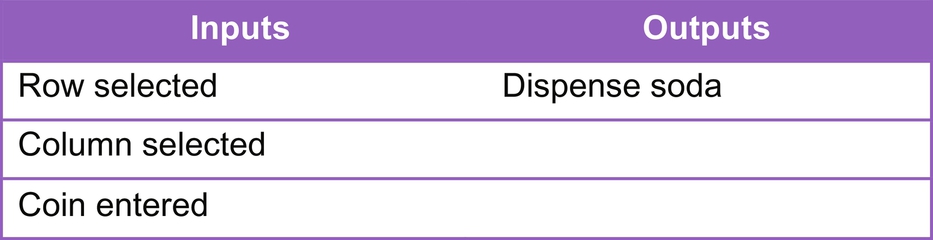
Our first task is to define inputs and outputs. Next, we will design the electronic interface with our inputs and outputs. Using the assessment of inputs and outputs, we have selected the PIC 10F200.
This will accommodate our program space, which will be quite short. As we do not need the comparator, we will be using the GPIO pins for our input and output. GP3 is input only. We will assign the “Coin Entered” pin as this input on GP3. Row selected will be GP0, with column selected as GP1. GP2 will be our “Dispense Soda” output.
- Program exercise2 (x: integer)
- ROW : integer := x;
- COLUMN : integer :=y;
- DISPENSESODA : (yes, no);
- COINRECEIVED : (yes, no);
- Begin
- ; assert 1 <= ROW <= 2
- ; assert 1 <= COLUMN <= 3
- ENDLESSLOOP Read ROW;
- Read COLUMN;
- Read COINRECEIVED;
- If COINRECEIVED = no,
- THEN DISPENSESODA := no;
- ELSEIF BEGIN
- DISPENSESODA := yes;
- CLOSE SWITCH Row, Column
- END
- ENDIF
- GOTO ENDLESSLOOP
- End.
Microchip Tools
Microchip’s most basic tools are available for free on their website, www.microchip.com. To get started, download MPLAB X Integrated Design Environment (IDE). Initially, you will want to use the simulator. Use tutorials to ensure you have the tools set up correctly.
Microchip Microcontroller Course Information
Microchip has an extensive network of field representatives that offer classes in each of the product families. To get up to speed quickly, look online at http://www.microchip.com for a local class on the particular family you are using. These courses are thorough, covering everything one needs to “fully develop and download applications” into Baseline, Midrange, and Midrange Enhanced microcontrollers (MCU). The courses are also very hands on and, also, give you time to put your new knowledge to use with an experiment on a personal computer (PC).
Course number MCU0101 is “Getting Started with Microchip Baseline PIC MCU Architecture and Peripherals.” This is a 2 class unit course.
Fundamentals of the Midrange are covered in three courses; MCU1101, MCU1102, MCU1121. MCU1101 (1 class unit) is entitled “Getting Started with Microchip’s Midrange Microcontroller Family Architecture” and includes information on the “programmer’s model, data and program memory organization, clocking structures, assembly language and special features of the devices.” This is also a hands-on course with MPLAB X IDE.
MCU1102 (1 class unit) is entitled “Getting Started with Microchip’s PIC16F1 Enhanced MCU Architecture.” Topics include “enhancements to the data and program memory, clocking schemes, and special features of the MCU.”
The final course, MCU1121 (2 class units) is entitled “Microchip Midrange PIC MCU Peripheral Configuration and Usage with C.” This course provides details on peripherals including timers, A/D converters, UARTs, and Comparators. This course is also quite hands on, with the MPLAB X IDE, learning to program in assembly, using development tools including simulators.
Jargon Note—Italics
Assembly language uses quite a few new terms. When a new term is introduced, it is highlighted with italics type and the surrounding material provides the definition with explanation.
Word Search

Binary Puzzle
Complete the grid so that each row and column contain four 0s and four 1s. The same number cannot appear in more than two consecutive squares in any row or column. Bonus: In the last column and the last row, write the hexadecimal value for each 8-bit column and row binary value (see Chapter 9).

How to solve Binary
The puzzle is to be completed with 8-bit binary values, placing the hexadecimal value of each row in the right-most column and placing the hexadecimal value of each column in the bottom-most row. Complete the grid so that each row contains four 0s and four 1s. Each column may contain three, four, or five 1s, with the balance in 0s. The same number cannot appear in more than two consecutive squares in any row or column. In the finished puzzle, each row must have a different sequence of 0s and 1s to any other row, and likewise for each column.
Further Reading
A presentation on the “Why?” of assembly language is shown on page 76–77 in Programming Structures, Volume 1 Machines and Programs, by Jan Hext, Section 5.3 Registers.
Program structure “mind-reading” exercise and outline of program from beginning to end is presented in Programming Structures by Jan Hext from page 136 to 137, Section 7.2 Program Structures.
Mathematical puzzles can be found at https://nrich.maths.org/1051, including the specific “mind-reading” algorithm.
The Microchip Data Sheet used for the perusal of a Data Sheet is 10F2xx (DS40001239F) from page 45 to 52. In the Practice Exercise, references are made to Data Sheets 12(L)F1571/2 (DS40001723D) from page 247 to 258; and Data Sheets 16(L)F1454/5/9 (DS40001639B) pages 330–341.
Two slides are presented from Mark McComb’s Technical Training Engineering Webinar from 2006, Slide 4 and Slide 6 of “Enhanced Mid-Range Architecture.”