
5 Basic Modeling Constructs
The description of a module in a digital system can be divided into two facets: the external view and the internal view. The external view describes the interface to the module, including the number and types of inputs and outputs. The internal view describes how the module implements its function. In VHDL, we can separate the description of a module into an entity declaration, which describes the external interface, and one or more architecture bodies, which describe alternative internal implementations. These were introduced in Chapter 1 and are discussed in detail in this chapter. We also look at how a design is processed in preparation for simulation or synthesis.
5.1 Entity Declarations
Let us first examine the syntax rules for an entity declaration and then show some examples. We start with a simplified description of entity declarations and move on to a full description later in this chapter. The syntax rules for this simplified form of entity declaration are

The identifier in an entity declaration names the module so that it can be referred to later. If the identifier is included at the end of the declaration, it must repeat the name of the entity. The port clause names each of the ports, which together form the interface to the entity. We can think of ports as being analogous to the pins of a circuit; they are the means by which information is fed into and out of the circuit. In VHDL, each port of an entity has a type, which specifies the kind of information that can be communicated, and a mode, which specifies whether information flows into or out from the entity through the port. These aspects of type and direction are in keeping with the strong typing philosophy of VHDL, which helps us avoid erroneous circuit descriptions. A simple example of an entity declaration is

This example describes an entity named adder, with two input ports and one output port, all of type word, which we assume is defined elsewhere. We can list the ports in any order; we do not have to put inputs before outputs. Also, we can include a list of ports of the same mode and type instead of writing them out individually. Thus the above declaration could equally well be written as follows:

In this example we have seen input and output ports. We can also have bidirectional ports, with mode inout. These can be used to model devices that alternately sense and drive data through a pin. Such models must deal with the possibility of more than one connected device driving a given signal at the same time. VHDL provides a mechanism for this, signal resolution, which we will return to in Chapter 11.
The similarity between the description of a port in an entity declaration and the declaration of a variable may be apparent. This similarity is not coincidental, and we can extend the analogy by specifying a default value on a port description, for example:

The default value, in this case the ‘1’ on the input ports, indicates the value each port should assume if it is left unconnected in an enclosing model. We can think of it as describing the value that the port “loats to." On the other hand, if the port is used, the default value is ignored. We say more about use of default values when we look at the execution of a model.
Another point to note about entity declarations is that the port clause is optional. So we can write an entity declaration such as
which describes a completely self-contained module. As the name in this example implies, this kind of module usually represents the top level of a design hierarchy.
Finally, if we return to the first syntax rule on page 108, we see that we can include declarations of items within an entity declaration. These include declarations of constants, types, signals and other kinds of items that we will see later in this chapter. The items can be used in all architecture bodies corresponding to the entity. Thus, it makes sense to include declarations that are relevant to the entity and all possible implementations. Anything that is part of only one particular implementation should instead be declared within the corresponding architecture body.
EXAMPLE
Suppose we are designing an embedded controller using a microprocessor with a program stored in a read-only memory (ROM). The program to be stored in the ROM is fixed, but we still need to model the ROM at different levels of detail. We can include declarations that describe the program in the entity declaration for the ROM, as shown in Figure 5-1. These declarations are not directly accessible to a user of the ROM entity, but serve to document the contents of the ROM. Each architecture body corresponding to the entity can use the constant program to initialize whatever structure it uses internally to implement the ROM.


FIGURE 5-1 An entity declaration for a ROM, including declarations that describe the program contained in it.
VHDL-87
The keyword entity may not be included at the end of an entity declaration in VHDL-87.
5.2 Architecture Bodies
The internal operation of a module is described by an architecture body. An architecture body generally applies some operations to values on input ports, generating values to be assigned to output ports. The operations can be described either by processes, which contain sequential statements operating on values, or by a collection of components representing sub-circuits. Where the operation requires generation of intermediate values, these can be described using signals, analogous to the internal wires of a module. The syntax rule for architecture bodies shows the general outline:

The identifier names this particular architecture body, and the entity name specifies which module has its operation described by this architecture body. If the identifier is included at the end of the architecture body, it must repeat the name of the architecture body. There may be several different architecture bodies corresponding to a single entity, each describing an alternative way of implementing the module’s operation. The block declarative items in an architecture body are declarations needed to implement the operations. The items may include type and constant declarations, signal declarations and other kinds of declarations that we will look at in later chapters.
Concurrent Statements
The concurrent statements in an architecture body describe the module’s operation. One form of concurrent statement, which we have already seen, is a process statement. Putting this together with the rule for writing architecture bodies, we can look at a simple example of an architecture body corresponding to the adder entity on page 108:

The architecture body is named abstract, and it contains a process add_a_b, which describes the operation of the entity. The process assumes that the operator + is defined for the type word, the type of a and b. We will see in Chapter 7 how such a definition may be written. We could also envisage additional architecture bodies describing the adder in different ways, provided they all conform to the external interface laid down by the entity declaration.
We have looked at processes first because they are the most fundamental form of concurrent statement. All other forms can ultimately be reduced to one or more processes. Concurrent statements are so called because conceptually they can be activated and perform their actions together, that is, concurrently. Contrast this with the sequential statements inside a process, which are executed one after another. Concurrency is useful for modeling the way real circuits behave. If we have two gates whose inputs change, each evaluates its new output independently of the other. There is no inherent sequencing governing the order in which they are evaluated. We look at process statements in more detail in Section 5.3. Then, in Section 5.4, we look at another form of concurrent statement, the component instantiation statement, used to describe how a module is composed of interconnected sub-modules.
Signal Declarations
When we need to provide internal signals in an architecture body, we must define them using signal declarations. The syntax for a signal declaration is very similar to that for a variable declaration:
This declaration simply names each signal, specifies its type and optionally includes an initial value for all signals declared by the declaration.
EXAMPLE
Figure 5-2 is an example of an architecture body for the entity and_or_inv, defined on page 109. The architecture body includes declarations of some signals that are internal to the architecture body. They can be used by processes within the architecture body but are not accessible outside, since a user of the module need not be concerned with the internal details of its implementation. Values are assigned to signals using signal assignment statements within processes. Signals can be sensed by processes to read their values.

FIGURE 5-2 An architecture body corresponding to the and_or_inv entity shown on page 109.
An important point illustrated by this example is that the ports of the entity are also visible to processes inside the architecture body and are used in the same way as signals. This corresponds to our view of ports as external pins of a circuit: from the internal point of view, a pin is just a wire with an external connection. So it makes sense for VHDL to treat ports like signals inside an architecture of the entity.
5.3 Behavioral Descriptions
At the most fundamental level, the behavior of a module is described by signal assignment statements within processes. We can think of a process as the basic unit of behavioral description. A process is executed in response to changes of values of signals and uses the present values of signals it reads to determine new values for other signals. A signal assignment is a sequential statement and thus can only appear within a process. In this section, we look in detail at the interaction between signals and processes.
Signal Assignment
In all of the examples we have looked at so far, we have used a simple form of signal assignment statement. Each assignment just provides a new value for a signal. The value is determined by evaluating an expression, the result of which must match the type of the signal. What we have not yet addressed is the issue of timing: when does the signal take on the new value? This is fundamental to modeling hardware, in which events occur over time. First, let us look at the syntax for a basic signal assignment statement in a process:

The optional label allows us to identify the statement. We will discuss labeled statements in Chapter 20. The syntax rules tell us that we can specify a delay mechanism, which we come to soon, and one or more waveform elements, each consisting of a new value and an optional delay time. It is these delay times in a signal assignment that allow us to specify when the new value should be applied. For example, consider the following assignment:
This specifies that the signal y is to take on the new value at a time 5 ns later than that at which the statement executes. The delay can be read in one of two ways, depending on whether the model is being used purely for its descriptive value or for simulation. In the first case, the delay can be considered in an abstract sense as a specification of the module’s propagation delay: whenever the input changes, the output is updated 5 ns later. In the second case, it can be considered in an operational sense, with reference to a host machine simulating operation of the module by executing the model. Thus if the above assignment is executed at time 250 ns, and or_a_b has the value ‘1’ at that time, then the signal y will take on the value ‘0’ at time 255 ns. Note that the statement itself executes in zero modeled time.
The time dimension referred to when the model is executed is simulation time, that is, the time in which the circuit being modeled is deemed to operate. This is distinct from real execution time on the host machine running a simulation. We measure simulation time starting from zero at the start of execution and increasing in discrete steps as events occur in the model. Not surprisingly, this technique is called discrete event simulation. A discrete event simulator must have a simulation time clock, and when a signal assignment statement is executed, the delay specified is added to the current simulation time to determine when the new value is to be applied to the signal. We say that the signal assignment schedules a transaction for the signal, where the transaction consists of the new value and the simulation time at which it is to be applied. When simulation time advances to the time at which a transaction is scheduled, the signal is updated with the new value. We say that the signal is active during that simulation cycle. If the new value is not equal to the old value it replaces on a signal, we say an event occurs on the signal. The importance of this distinction is that processes respond to events on signals, not to transactions.
The syntax rules for signal assignments show that we can schedule a number of transactions for a signal, to be applied after different delays. For example, a clock driver process might execute the following assignment to generate the next two edges of a clock signal (assuming T_pw is a constant that represents the clock pulse width):
If this statement is executed at simulation time 50 ns and T_pw has the value 10 ns, one transaction is scheduled for time 60 ns to set clk to ‘1’, and a second transaction is scheduled for time 70 ns to set clk to ‘0’. If we assume that clk has the value ‘0’ when the assignment is executed, both transactions produce events on clk.
This signal assignment statement shows that when more than one transaction is included, the delays are all measured from the current time, not the time in the previous element. Furthermore, the transactions in the list must have strictly increasing delays, so that the list reads in the order that the values will be applied to the signal.
EXAMPLE
We can write a process declaration for a clock generator using the above signal assignment statement to generate a symmetrical clock signal with pulse width T_pw. The difficulty is to get the process to execute regularly every clock cycle. One way to do this is by making it resume whenever the clock changes and scheduling the next two transitions when it changes to ‘0’. This approach is shown in Figure 5-3.

FIGURE 5-3 A process that generates a symmetric clock waveform.
Since a process is the basic unit of a behavioral description, it makes intuitive sense to be allowed to include more than one signal assignment statement for a given signal within a single process. We can think of this as describing the different ways in which a signal’s value can be generated by the process at different times.
EXAMPLE
We can write a process that models a two-input multiplexer as shown in Figure 5-4. The value of the sel port is used to select which signal assignment to execute to determine the output value.

FIGURE 5-4 A process that models a two-input multiplexer.
We say that a process defines a driver for a signal if and only if it contains at least one signal assignment statement for the signal. So this example defines a driver for the signal z. If a process contains signal assignment statements for several signals, it defines drivers for each of those signals. A driver is a source for a signal in that it provides values to be applied to the signal. An important rule to remember is that for normal signals, there may only be one source. This means that we cannot write two different processes each containing signal assignment statements for the one signal. If we want to model such things as buses or wired-or signals, we must use a special kind of signal called a resolved signal, which we will discuss in Chapter 11.
VHDL-87
Signal assignment statements may not be labeled in VHDL-87.
Signal Attributes
In Chapter 2 we introduced the idea of attributes of types, which give information about allowed values for the types. Then, in Chapter 4, we saw how we could use attributes of array objects to get information about their index ranges. We can also refer to attributes of signals to find information about their history of transactions and events. Given a signal S, and a value T of type time, VHDL defines the following attributes:
The first three attributes take an optional time parameter. If we omit the parameter, the value 0 fs is assumed. These attributes are often used in checking the timing behavior within a model. For example, we can verify that a signal d meets a minimum setup time requirement of Tsu before a rising edge on a clock clk of type std_ulogic as follows:

Similarly, we might check that the pulse width of a clock signal input to a module doesn’t exceed a maximum frequency by testing its pulse width:
Note that we test the time since the last event on a delayed version of the clock signal. When there is currently an event on a signal, the ‘last_event attribute returns the value 0 fs. In this case, we determine the time since the previous event by applying the ‘last_event attribute to the signal delayed by 0 fs. We can think of this as being an infinitesimal delay. We will return to this idea later in this chapter, in our discussion of delta delays.
EXAMPLE
We can use a similar test for the rising edge of a clock signal to model an edge-triggered module, such as a flipflop. The flipflop should load the value of its D input on a rising edge of clk, but asynchronously clear the outputs whenever clr is ‘1’ The entity declaration and a behavioral architecture body are shown in Figure 5-5.

If the flipflop did not have the asynchronous clear input, the model could have used a simple wait statement such as
to trigger on a rising edge. However, with the clear input present, the process must be sensitive to changes on both clk and clr at any time. Hence it uses the ‘event attribute to distinguish between clk changing to ‘1’ and clr going back to ‘0’ while clk is stable at ‘1’.
VHDL-87
In VHDL-87, the ‘last_value attribute for a composite signal returns the aggregate of last values for each of the scalar elements of the signal. For example, suppose a bit-vector signal s initially has the value B"00" and changes to B"01" and then B"11" in successive events. After the last event, the result of s’last_value is B"00" in VHDL-87. In VHDL-93 and VHDL-2001 it is B"01", since that is the last value of the entire composite signal.
Wait Statements
Now that we have seen how to change the values of signals over time, the next step in behavioral modeling is to specify when processes respond to changes in signal values. This is done using wait statements. A wait statement is a sequential statement with the following syntax rule:

The optional label allows us to identify the statement. We will discuss labeled statements in Chapter 20. The purpose of the wait statement is to cause the process that executes the statement to suspend execution. The sensitivity clause, condition clause and timeout clause specify when the process is subsequently to resume execution. We can include any combination of these clauses, or we may omit all three. Let us go through each clause and describe what it specifies.
The sensitivity clause, starting with the word on, allows us to specify a list of signals to which the process responds. If we just include a sensitivity clause in a wait statement, the process will resume whenever any one of the listed signals changes value, that is, whenever an event occurs on any of the signals. This style of wait statement is useful in a process that models a block of combinatorial logic, since any change on the inputs may result in new output values; for example:

The process starts execution by generating values for sum and carry based on the initial values of a and b, then suspends on the wait statement until either a or b (or both) change values. When that happens, the process resumes and starts execution from the top.
This form of process is so common in modeling digital systems that VHDL provides the shorthand notation that we have seen in many examples in preceding chapters, A process with a sensitivity list in its heading is exactly equivalent to a process with a wait statement at the end, containing a sensitivity clause naming the signals in the sensitivity list. So the half_add process above could be rewritten as

EXAMPLE
Let us return to the model of a two-input multiplexer shown in Figure 5-4. The process in that model is sensitive to all three input signals. This means that it will resume on changes on either data input, even though only one of them is selected at any time. If we are concerned about this slight lack of efficiency in simulation, we can write the process differently, using wait statements to be more selective about the signals to which the process is sensitive each time it suspends. The revised model is shown in Figure 5-6. In this model, when input a is selected, the process only waits for changes on the select input and on a. Any changes on b are ignored. Similarly, if b is selected, the process waits for changes on sel and on b, ignoring changes on a.

FIGURE 5-6 An entity and architecture body for a multiplexer that avoids being resumed in response to changes on the input signal that is not currently selected.
The condition clause in a wait statement, starting with the word until, allows us to specify a condition that must be true for the process to resume. For example, the wait statement
causes the executing process to suspend until the value of the signal clk changes to ‘1’. The condition expression is tested while the process is suspended to determine whether to resume the process. A consequence of this is that even if the condition is true when the wait statement is executed, the process will still suspend until the appropriate signals change and cause the condition to be true again. If the wait statement doesn’t include a sensitivity clause, the condition is tested whenever an event occurs on any of the signals mentioned in the condition.
EXAMPLE
The clock generator process from the example on page 114 can be rewritten using a wait statement with a condition clause, as shown in Figure 5-7. Each time the process executes the wait statement, clk has the value ‘0’. However, the process still suspends, and the condition is tested each time there is an event on clk. When clk changes to ‘1’, nothing happens, but when it changes to ‘0’ again, the process resumes and schedules transactions for the next cycle.

FIGURE 5-7 The revised clock generator process.
If a wait statement includes a sensitivity clause as well as a condition clause, the condition is only tested when an event occurs on any of the signals in the sensitivity clause. For example, if a process suspends on the following wait statement:
the condition is tested on each change in the value of clk, regardless of any changes on reset.
The timeout clause in a wait statement, starting with the word for, allows us to specify a maximum interval of simulation time for which the process should be suspended. If we also include a sensitivity or condition clause, these may cause the process to be resumed earlier. For example, the wait statement
causes the executing process to suspend until trigger changes to ‘1’, or until 1 ms of simulation time has elapsed, whichever comes first. If we just include a timeout clause by itself in a wait statement, the process will suspend for the time given.
EXAMPLE
We can rewrite the clock generator process from the example on page 114 yet again, this time using a wait statement with a timeout clause, as shown in Figure 5-8. In this case we specify the clock period as the timeout, after which the process is to be resumed.

FIGURE 5-8 A third version of the clock generator process.
If we refer back to the syntax rule for a wait statement shown on page 118, we note that it is legal to write
This form causes the executing process to suspend for the remainder of the simulation. Although this may at first seem a strange thing to want to do, in practice it is quite useful. One place where it is used is in a process whose purpose is to generate stimuli for a simulation. Such a process should generate a sequence of transactions on signals connected to other parts of a model and then stop. For example, the process

generates all four possible combinations of values on the signals testO and testl. If the final wait statement were omitted, the process would cycle forever, repeating the signal assignment statements without suspending, and the simulation would make no progress.
VHDL-87
Wait statements may not be labeled in VHDL-87.
Delta Delays
Let us now return to the topic of delays in signal assignments. In many of the example signal assignments in previous chapters, we omitted the delay part of waveform elements. This is equivalent to specifying a delay of 0 fs. The value is to be applied to the signal at the current simulation time. However, it is important to note that the signal value does not change as soon as the signal assignment statement is executed. Rather, the assignment schedules a transaction for the signal, which is applied after the process suspends. Thus the process does not see the effect of the assignment until the next time it resumes, even if this is at the same simulation time. For this reason, a delay of 0 fs in a signal assignment is called a delta delay.
To understand why delta delays work in this way, it is necessary to review the simulation cycle, introduced in Chapter 1 on page 15. Recall that the simulation cycle consists of two phases: a signal update phase followed by a process execution phase. In the signal update phase, simulation time is advanced to the time of the earliest scheduled transaction, and the values in all transactions scheduled for this time are applied to their corresponding signals. This may cause events to occur on some signals. In the process execution phase, all processes that respond to these events are resumed and execute until they suspend again on wait statements. The simulator then repeats the simulation cycle.
Let us now consider what happens when a process executes a signal assignment statement with delta delay, for example:
Suppose this is executed at simulation time t during the process execution phase of the current simulation cycle. The effect of the assignment is to schedule a transaction to put the value X"00" on data at time t. The transaction is not applied immediately, since the simulator is in the process execution phase. Hence the process continues executing, with data unchanged. When all processes have suspended, the simulator starts the next simulation cycle and updates the simulation time. Since the earliest transaction is now at time t, simulation time remains unchanged. The simulator now applies the value X"00" in the scheduled transaction to data, then resumes any processes that respond to the new value.
Writing a model with delta delays is useful when we are working at a high level of abstraction and are not yet concerned with detailed timing. If all we are interested in is describing the order in which operations take place, delta delays provide a means of ignoring the complications of timing. We have seen this in many of the examples in previous chapters. However, we should note a common pitfall encountered by most beginner VHDL designers when using delta delays: they forget that the process does not see the effect of the assignment immediately. For example, we might write a process that includes the following statements:
and expect the process to execute the if statement assuming s has the value ‘1’. We would then spend fruitless hours debugging our model until we remembered that s still has its old value until the next simulation cycle, after the process has suspended.
EXAMPLE
Figure 5-9 is an outline of an abstract model of a computer system. The CPU and memory are connected with address and data signals. They synchronize their operation with the mem_read and mem_write control signals and the mem_ready status signal. No delays are specified in the signal assignment statements, so synchronization occurs over a number of delta delay cycles, as shown in Figure 5-10.

FIGURE 5-9 An outline of an abstract model for a computer system, consisting of a CPU and a memory. The proc- esses use delta delays to synchronize communication, rather than modeling timing of bus transactions in detail.

FIGURE 5-10 Synchronization over successive delta cycles in a simulation of a read operation between the CPU and memory shown in Figure 5-9.
When the simulation starts, the CPU process begins executing its statements and the memory suspends. The CPU schedules transactions to assign the next instruction address to the address signal and the value ‘1’ to the mem_read signal, then suspends. In the next simulation cycle, these signals are updated and the memory process resumes, since it is waiting for an event on mem_read. The memory process schedules the data on the read_data signal and the value ‘1’ on mem_ready, then suspends. In the third cycle, these signals are updated and the CPU process resumes. It schedules the value ‘0’ on mem_read and suspends. Then, in the fourth cycle, mem_read is updated and the memory process is resumed, scheduling the value ‘0’ on mem_ready to complete the handshake. Finally, on the fifth cycle, mem_ready is updated and the CPU process resumes and executes the fetched instruction.
Transport and Inertial Delay Mechanisms
So far in our discussion of signal assignments, we have implicitly assumed that there were no pending transactions scheduled for a signal when a signal assignment statement was executed. In many models, particularly at higher levels of abstraction, this will be the case. If, on the other hand, there are pending transactions, the new transactions are merged with them in a way that depends on the delay mechanism used in the signal assignment statement. This is an optional part of the signal assignment syntax shown on page 113. The syntax rule for the delay mechanism is
A signal assignment with the delay mechanism part omitted is equivalent to specifying inertial. We look at the transport delay mechanism first, since it is simpler, and then return to the inertial delay mechanism.
We use the transport delay mechanism when we are modeling an ideal device with infinite frequency response, in which any input pulse, no matter how short, produces an output pulse. An example of such a device is an ideal transmission line, which transmits all input changes delayed by some amount. A process to model a transmission line with delay 500 ps is

In this model the output follows any changes in the input, but delayed by 500 ps. If the input changes twice or more within a period shorter than 500 ps, the scheduled transactions are simply queued by the driver until the simulation time at which they are to be applied, as shown in Figure 5-11.
In this example, each new transaction that is generated by a signal assignment statement is scheduled for a simulation time that is later than the pending transactions queued by the driver. The situation gets a little more complex when variable delays are used, since we can schedule a transaction for an earlier time than a pending transaction. The semantics of the transport delay mechanism specify that if there are pending transactions on a driver that are scheduled for a time later than or equal to a new transaction, those later transactions are deleted.

Figure 5-11 Transactions queued by a driver using transport delay. At time 200 ps the input changes, and a transaction is scheduled for 700 ps. At time 500 ps, the input changes again, and another transaction is scheduled for 1000 ps. This is queued by the driver behind the earlier transaction. When simulation time reaches 700 ps, the first transaction is applied, and the second transaction remains queued. Finally, simulation time reaches 1000 ps, and the final transaction is applied, leaving the driver queue empty.
EXAMPLE
Figure 5-12 is a process that describes the behavior of an asymmetric delay element, with different delay times for rising and falling transitions. The delay for rising transitions is 800 ps and for falling transitions 500 ps. If we apply an input pulse of only 200 ps duration, we would expect the output not to change, since the delayed falling transition should “vertake" the delayed rising transition. If we were simply to add each transition to the driver queue when a signal assignment statement is executed, we would not get this behavior. However, the semantics of the transport delay mechanism produce the desired behavior, as Figure 5-13 shows.

FIGURE 5-12 A process that describes a delay element with asymmetric delays for rising and falling transitions.

FIGURE 5-13 Transactions in a driver using asymmetric transport delay. At time 200 ps the input changes, and a transaction is scheduledfor 1000 ps. At time 400 ps, the input changes again, and another transaction is scheduled for 900 ps. Since this is earlier than the pending transaction at 1000 ps, the pending transaction is deleted. When simulation time reaches 900 ps, the remaining transaction is applied, but since the value is ‘0’, no event occurs on the signal.
Most real electronic circuits don’t have infinite frequency response, so it is not appropriate to model them using transport delay. In real devices, changing the values of internal nodes and outputs involves moving electronic charge around in the presence of capacitance, inductance and resistance. This gives the device some inertia; it tends to stay in the same state unless we force it by applying inputs for a sufficiently long duration. This is why VHDL includes the inertial delay mechanism, to allow us to model devices that reject input pulses too short to overcome their inertia. Inertial delay is the mechanism used by default in a signal assignment, or we can specify it explicitly by including the word inertial.
To explain how inertial delay works, let us first consider a model in which all the signal assignments for a given signal use the same delay value, say, 3 ns, as in the following inverter model:

So long as input events occur more than 3 ns apart, this model does not present any problems. Each time a signal assignment is executed, there are no pending transactions, so a new transaction is scheduled, and the output changes value 3 ns later. However, if an input changes less than 3 ns after the previous change, this represents a pulse less than the propagation delay of the device, so it should be rejected. This behavior is shown at the top of Figure 5-14. In a simple model such as this, we can interpret inertial delay as saying if a signal assignment would produce an output pulse shorter than the propagation delay, then the output pulse does not happen.

FIGURE 5-14 Results of signal assignments using the inertial delay mechanism. In the top waveform, an inertial delay of 3 ns is specified. The input change at time 1 ns is reflected in the output at time 4 ns. The pulse from 6 to 8 ns is less than the propagation delay, so it doesn’t affect the output. In the bottom waveform, an inertial delay of 3 ns and a pulse rejection limit of 2 ns are specified. The input changes at 1, 6, 9 and 11.5 ns are all reflected in the output, since they occur greater than 2 ns apart. However, the subsequent input pulses are less than or equal to the pulse rejection limit in length, and so do not affect the output.
Next, let us extend this model by specifying a pulse rejection limit, after the word reject in the signal assignment:

We can interpret this as saying if a signal assignment would produce an output pulse shorter than (or equal to) the pulse rejection limit, the output pulse does not happen. In this simple model, so long as input changes occur more than 2 ns apart, they produce output changes 3 ns later, as shown at the bottom of Figure 5-14. Note that the pulse rejection limit specified must be between 0 fs and the delay specified in the signal assignment. Omitting a pulse rejection limit is the same as specifying a limit equal to the delay, and specifying a limit of 0 fs is the same as specifying transport delay.
Now let us look at the full story of inertial delay, allowing for varying the delay time and pulse rejection limit in different signal assignments applied to the same signal. As with transport delay, the situation becomes more complex, and it is best to describe it in terms of deleting transactions from the driver. Those who are unlikely to be writing models that deal with timing at this level of detail may wish to move on to the next section.
An inertially delayed signal assignment involves examining the pending transactions on a driver when adding a new transaction. Suppose a signal assignment schedules a new transaction for time tnew, with a pulse rejection limit of tr. First, any pending transactions scheduled for a time later than or equal to tnew are deleted, just as they are when transport delay is used. Then the new transaction is added to the driver. Second, any pending transactions scheduled in the interval tnew - tr to tnew are examined. If there is a run of consecutive transactions immediately preceding the new transaction with the same value as the new transaction, they are kept in the driver. All other transactions in the interval are deleted.
An example will make this clearer. Suppose a driver for signal s contains pending transactions as shown at the top of Figure 5-15, and the process containing the driver executes the following signal assignment statement at time 10 ns:
The pending transactions after this assignment are shown at the bottom of Figure 5-15.
One final point to note about specifying the delay mechanism in a signal assignment statement is that if a number of waveform elements are included, the specified mechanism only applies to the first element. All the subsequent elements schedule transactions using transport delay. Since the delays for multiple waveform elements must be in ascending order, this means that all of the transactions after the first are just added to the driver transaction queue in the order written.

FIGURE 5-15 Transactions before (top) and after (bottom) an inertial delay signal assignment. The transactions at 20 and 25 ns are deleted because they are scheduled for later than the new transaction. Those at 11 and 12 ns are retained because theyfall before the pulse rejection interval. The transactions at 16 and 17 ns fall within the rejection interval, but they form a run leading up to the new transaction, with the same value as the new transaction; hence they are also retained. The other transactions in the rejection interval are deleted.
EXAMPLE
A detailed model of a two-input and gate is shown in Figure 5-16. When a change on either of the input signals results in a change scheduled for the output, the delay process determines the propagation delay to be used. On a rising output transition, spikes of less than 400 ps are rejected, and on a falling or unknown transition, spikes of less than 300 ps are rejected. Note that the result of the and operator, when applied to standard-logic values, is always ‘U’, ‘X’, ‘0’ or ‘1’. Hence the delay process need not compare result with ‘H’ or ‘L’ when testing for rising or falling transitions.


Figure 5-16 An entity and architecture body fora two-input and gate. The process gate implements the logical function of the entity, and the process delay implements its detailed timing characteristics using inertially delayed signal assignments. A delay of 1.5 ns is used for rising transitions, 1.2 ns for falling transitions.
VHDL-87
VHDL-87 does not allow specification of the pulse rejection limit in a delay mechanism. The syntax rule in VHDL-87 is
If the delay mechanism is omitted, inertial delay is used, with a pulse rejection limit equal to the delay specified in the waveform element.
Process Statements
We have been using processes quite extensively in examples in this and previous chapters, so we have seen most of the details of how they are written and used. To summarize, let us now look at the formal syntax for a process statement and review process operation. The syntax rule is

Recall that a process statement is a concurrent statement that can be included in an architecture body to implement all or part of the behavior of a module. The process label identifies the process. While it is optional, it is a good idea to include a label on each process. A label makes it easier to debug a simulation of a system, since most simulators provide a way of identifying a process by its label. Most simulators also generate a default name for a process if we omit the label in the process statement. Having identified a process, we can examine the contents of its variables or set breakpoints at statements within the process.
The declarative items in a process statement may include constant, type and variable declarations, as well as other declarations that we will come to later. Note that ordinary variables may only be declared within process statements, not outside of them. The variables are used to represent the state of the process, as we have seen in the examples. The sequential statements that form the process body may include any of those that we introduced in Chapter 3, plus signal assignment and wait statements. When a process is activated during simulation, it starts executing from the first sequential statement and continues until it reaches the last. It then starts again from the first. This would be an infinite loop, with no progress being made in the simulation, if it were not for the inclusion of wait statements, which suspend process execution until some relevant event occurs. Wait statements are the only statements that take more than zero simulation time to execute. It is only through the execution of wait statements that simulation time advances.
A process may include a sensitivity list in parentheses after the keyword process. The sensitivity list identifies a set of signals that the process monitors for events. If the sensitivity list is omitted, the process should include one or more wait statements. On the other hand, if the sensitivity list is included, then the process body cannot include any wait statements. Instead, there is an implicit wait statement, just before the end process keywords, that includes the signals listed in the sensitivity list as signals in an on clause.
VHDL-87
The keyword is may not be included in the header of a process statement in VHDL-87.
Concurrent Signal Assignment Statements
The form of process statement that we have been using is the basis for all behavioral modeling in VHDL, but for simple cases, it can be a little cumbersome and verbose. For this reason, VHDL provides us with some useful shorthand notations for functional modeling, that is, behavioral modeling in which the operation to be described is a simple combinatorial transformation of inputs to an output. We look at the basic form of two of these statements, concurrent signal assignment statements, which are concurrent statements that are essentially signal assignments. Unlike ordinary signal assignments, concurrent signal assignment statements can be included in the statement part of an architecture body. The syntax rule is

which tells us that the two forms are called a conditional signal assignment and a selected signal assignment. Each of them may include a label, which serves exactly the same purpose as a label on a process statement: it allows the statement to be identified by name during simulation or synthesis.
Conditional Signal Assignment Statements
The conditional signal assignment statement is a shorthand for a collection of ordinary signal assignments contained in an if statement, which is in turn contained in a process statement. The simplified syntax rule for a conditional signal assignment is

The conditional signal assignment allows us to specify which of a number of waveforms should be assigned to a signal depending on the values of some conditions. Let us look at some examples and show how each conditional signal assignment can be transformed into an equivalent process statement. First, the top statement in Figure 5-17 is a functional description of a multiplexer, with four data inputs (d0, d1, d2 and d3), two select inputs (sel0 and se|l) and a data output (z). All of these signals are of type bit. This statement has exactly the same meaning as the process statement shown at the bottom of Figure 5-17.
The advantage of the conditional signal assignment form over the equivalent process is clearly evident from this example. The simple combinatorial transformation is obvious to the reader, uncluttered by the details of the process mechanism. This is not to say that processes are a bad thing, rather that in simple cases, we would rather hide that detail to make the model clearer. Looking at the equivalent process shows us something important about the conditional signal assignment statement, namely, that it is sensitive to all of the signals mentioned in the waveforms and the conditions. So whenever any of these change value, the conditional assignment is reevaluated and a new transaction scheduled on the driver for the target signal.

FIGURE 5-17 Top: a functional model of a multiplexer, using a conditional signal assignment statement. Bottom: the equivalent process statement.
If we look more closely at the multiplexer model, we note that the last condition is redundant, since the signals seO and sel are of type bit. If none of the previous conditions are true, the signal should always be assigned the last waveform. So we can rewrite the example as shown in Figure 5-18.
A very common case in function modeling is to write a conditional signal assignment with no conditions, as in the following example:
At first sight this appears to be an ordinary sequential signal assignment statement, which by rights ought to be inside a process body. However, if we look at the syntax rule for a concurrent signal assignment, we note that this can in fact be recognized as such if all of the optional parts except the label are omitted. In this case, the equivalent process statement is


FIGURE 5-18 A revised functional model for the multiplexer, with its equivalent process statement.
Another case that sometimes arises when writing functional models is the need for a process that schedules an initial set of transactions and then does nothing more for the remainder of the simulation. An example is the generation of a reset signal. One way of doing this is as follows:
The thing to note here is that there are no signals named in any of the waveforms or the conditions (assuming that extended_reset is a constant). This means that the statement is executed once when simulation starts, schedules two transactions on reset and remains quiescent thereafter. The equivalent process is

Since there are no signals involved, the wait statement has no sensitivity clause. Thus after the if statement has executed, the process suspends forever.
If we include a delay mechanism specification in a conditional signal assignment statement, it is used whichever waveform is chosen. So we might rewrite the model for the asymmetric delay element shown in Figure 5-12 as
One problem with conditional signal assignments, as we have described them so far, is that they always assign a new value to a signal. Sometimes we may not want to change the value of a signal, or more specifically, we may not want to schedule any new transactions on the signal. We can use the keyword unaffected instead of a normal waveform for these cases, as shown at the top of Figure 5-19.


FIGURE 5-19 Top: a conditional signal assignment statement showing use of the unaffected waveform. Bottom: the equivalent process statement.
The effect of the unaffected waveform is to include a null statement in the equivalent process, causing it to bypass scheduling a transaction when the corresponding condition is true. (Recall that the effect of the null sequential statement is to do nothing.) So the example at the top of Figure 5-19 is equivalent to the process shown at the bottom. Note that we can only use unaffected in a concurrent signal assignment, not in a sequential signal assignment.
VHDL-87
In VHDL-87 the syntax rule for a conditional signal assignment statement is

The delay mechanism is restricted to the keyword transport, as discussed on page 130. The final waveform may not be conditional. Furthermore, we may not use the keyword unaffected. If the required behavior cannot be expressed with these restrictions, we must write a full process statement instead of a conditional signal assignment statement.
Selected Signal Assignment Statements
The selected signal assignment statement is similar in many ways to the conditional signal assignment statement. It, too, is a shorthand for a number of ordinary signal assignments embedded in a process. But for a selected signal assignment, the equivalent process contains a case statement instead of an if statement. The simplified syntax rule is

This statement allows us to choose between a number of waveforms to be assigned to a signal depending on the value of an expression. As an example, let us consider the selected signal assignment shown at the top of Figure 5-20. This has the same meaning as the process statement containing a case statement shown at the bottom of Figure 5-20.
A selected signal assignment statement is sensitive to all of the signals in the selector expression and in the waveforms. This means that the selected signal assignment in Figure 5-20 is sensitive to b and will resume if b changes value, even if the value of alu_function is alu_pass_a.
An important point to note about a selected signal assignment statement is that the case statement in the equivalent process must be legal according to all of the rules that we described in Chapter 3. This means that every possible value for the selector expression must be accounted for in one of the choices, that no value is included in more than one choice and so on.
Apart from the difference in the equivalent process, the selected signal assignment is similar to the conditional assignment. Thus the special waveform unaffected can be used to specify that no assignment take place for some values of the selector expression. Also, if a delay mechanism is specified in the statement, that mechanism is used on each sequential signal assignment within the equivalent process.

FIGURE 5-20 Top: a selected signal assignment statement. Bottom: its equivalent process statement.
EXAMPLE
We can use a selected signal assignment to express a combinatorial logic function in truth-table form. Figure 5-21 shows an entity declaration and an architecture body for a full adder. The selected signal assignment statement has, as its selector expression, a bit vector formed by aggregating the input signals. The choices list all possible values of inputs, and for each, the values for the c_out and s outputs are given.

FIGURE 5-21 An entity declaration and functional architecture body for a full adder.
This example illustrates the most common use of aggregate targets in signal assignments. Note that the type qualification is required in the selector expression to specify the type of the aggregate. The type qualification is needed in the output values to distinguish the bit-vector string literals from character string literals.
VHDL-87
In VHDL-87, the delay mechanism is restricted to the keyword transport, as discussed on page 130. Furthermore, the keyword unaffected may not be used. If the required behavior cannot be expressed without using the keyword unaffected, we must write a full process statement instead of a selected signal assignment statement.
Concurrent Assertion Statements
VHDL provides another shorthand process notation, the concurrent assertion statement, which can be used in behavioral modeling. As its name implies, a concurrent assertion statement represents a process whose body contains an ordinary sequential assertion statement. The syntax rule is

This syntax appears to be exactly the same as that for a sequential assertion statement, but the difference is that it may appear as a concurrent statement. The optional label on the statement serves the same purpose as that on a process statement: to provide a way of referring to the statement during simulation or synthesis. The process equivalent to a concurrent assertion contains a sequential assertion with the same condition, report clause and severity clause. The sequential assertion is then followed by a wait statement whose sensitivity list includes the signals mentioned in the condition expression. Thus the effect of the concurrent assertion statement is to check that the condition holds true each time any of the signals mentioned in the condition change value. Concurrent assertions provide a very compact and useful way of including timing and correctness checks in a model.
EXAMPLE
We can use concurrent assertion statements to check for correct use of a set/reset flipflop, with two inputs s and r and two outputs q and q_n, all of type bit. The requirement for use is that s and r are not both ‘1’ at the same time. The entity and architecture body are shown in Figure 5-22.
The first and second concurrent statements implement the functionality of the model. The third checks for correct use and is resumed when either s or r changes value, since these are the signals mentioned in the Boolean condition. If both of the signals are ‘1’, an assertion violation is reported. The equivalent process for the concurrent assertion is


FIGURE 5-22 An entity and architecture body for a set/reset flipflop, including a concurrent assertion statement to check for correct usage.
Entities and Passive Processes
We complete this section on behavioral modeling by returning to declarations of entities. We can include certain kinds of concurrent statements in an entity declaration, to monitor use and operation of the entity. The extended syntax rule for an entity declaration that shows this is

The concurrent statements included in an entity declaration must be passive; that is, they may not affect the operation of the entity in any way. A concurrent assertion statement meets this requirement, since it simply tests a condition whenever events occur on signals to which it is sensitive. A process statement is passive if it contains no signal assignment statements or calls to procedures containing signal assignment statements. Such a process can be used to trace events that occur on the entity’s inputs. We will describe the remaining alternative, concurrent procedure call statements, when we discuss procedures in Chapter 7. A concurrent procedure call is passive if the procedure called contains no signal assignment statements or calls to procedures containing signal assignment statements.
EXAMPLE
We can rewrite the entity declaration for the set/reset flipflop of Figure 5-22 as shown in Figure 5-23. If we do this, the check is included for every possible implementation of the flipflop and does not need to be included in the corresponding architecture bodies.

EXAMPLE
Figure 5-24 shows an entity declaration for a read-only memory (ROM). It includes a passive process, trace_reads, that is sensitive to changes on the enable port. When the value of the port changes to ‘1’, the process reports a message tracing the time and address of the read operation. The process does not affect the course of the simulation in any way, since it does not include any signal assignments.

FIGURE 5-24 An entity declaration for a ROM, including a passive process for tracing read operations.
5.4 Structural Descriptions
A structural description of a system is expressed in terms of subsystems interconnected by signals. Each subsystem may in turn be composed of an interconnection of sub-subsystems, and so on, until we finally reach a level consisting of primitive components, described purely in terms of their behavior. Thus the top-level system can be thought of as having a hierarchical structure. In this section, we look at how to write structural architecture bodies to express this hierarchical organization.
Component Instantiation and Port Maps
We have seen earlier in this chapter that the concurrent statements in an architecture body describe an implementation of an entity interface. In order to write a structural implementation, we must use a concurrent statement called a component instantiation statement, the simplest form of which is governed by the syntax rule

This form of component instantiation statement performs direct instantiation of an entity. We can think of component instantiation as creating a copy of the named entity, with the corresponding architecture body substituted for the component instance. The port map specifies which ports of the entity are connected to which signals in the enclosing architecture body. The simplified syntax rule for a port association list is
Each element in the association list associates one port of the entity either with one signal of the enclosing architecture body or with the value of an expression, or leaves the port unassociated, as indicated by the keyword open.
Let us look at some examples to illustrate component instantiation statements and the association of ports with signals. Suppose we have an entity declared as

and a corresponding architecture called fpld. We might create an instance of this entity as follows:
In this example, the name work refers to the current working library in which entities and architecture bodies are stored. We return to the topic of libraries in the next section. The port map of this example lists the signals in the enclosing architecture body to which the ports of the copy of the entity are connected. Positional association is used: each signal listed in the port map is connected to the port at the same position in the entity declaration. So the signal cpu_rd is connected to the port rd, the signal cpu_wr is connected to the port wr and so on.
One of the problems with positional association is that it is not immediately clear which signals are being connected to which ports. Someone reading the description must refer to the entity declaration to check the order of the ports in the entity interface. A better way of writing a component instantiation statement is to use named association, as shown in the following example:

Here, each port is explicitly named along with the signal to which it is connected. The order in which the connections are listed is immaterial. The advantage of this approach is that it is immediately obvious to the reader how the entity is connected into the structure of the enclosing architecture body.
In the preceding example we have explicitly named the architecture body to be used corresponding to the entity instantiated. However, the syntax rule for component instantiation statements shows this to be optional. If we wish, we can omit the specification of the architecture body, in which case the one to be used may be chosen when the overall model is processed for simulation, synthesis or some other purpose. At that time, if no other choice is specified, the most recently analyzed architecture body is selected. We return to the topic of analyzing models in the next section.
EXAMPLE
In Figure 5-5 we looked at a behavioral model of an edge-triggered flipflop. We can use the flipflop as the basis of a four-bit edge-triggered register. Figure 5-25 shows the entity declaration and a structural architecture body.

FIGURE 5-25 An entity and structural architecture body for a four-bit edge-triggered register, with an asynchronous clear input.
We can use the register entity, along with other entities, as part of a structural architecture for the two-digit decimal counter represented by the schematic of Figure 5-26. Suppose a digit is represented as a bit vector of length four, described by the subtype declaration
Figure 5-27 shows the entity declaration for the counter, along with an outline of the structural architecture body. This example illustrates a number of important points about component instances and port maps. First, the two component instances val0_reg and val1_reg are both instances of the same entity/architecture pair. This means that two distinct copies of the architecture struct of reg4 are created, one for each of the component instances. We return to this point when we discuss the topic of elaboration in the next section. Second, in each of the port maps, ports of the entity being instantiated are associated with separate elements of array signals. This is allowed, since a signal that is of a composite type, such as an array, can be treated as a collection of signals, one per element. Third, some of the signals connected to the component instances are signals declared within the enclosing architecture body, registered, whereas the clk signal is a port of the entity counter. This again illustrates the point that within an architecture body, the ports of the corresponding entity are treated as signals.

FIGURE 5-26 A schematic for a two-digit counter using the reg4 entity.

FIGURE 5-27 An entity declaration of a two-digit decimal counter, with an outline of an architecture body using the reg4 entity.
We saw in the above example that we can associate separate ports of an instance with individual elements of an actual signal of a composite type, such as an array or record type. If an instance has a composite port, we can write associations the other way around; that is, we can associate separate actual signals with individual elements of the port. This is sometimes called subelement association. For example, if the instance DMA_buffer has a port status of type FIFO_status, declared as
we could associate a signal with each element of the port as follows:

This illustrates two important points about subelement association. First, all elements of the composite port must be associated with an actual signal. We cannot associate some elements and leave the rest unassociated. Second, all of the associations for a particular port must be grouped together in the association list, without any associations for other ports among them.
We can use subelement association for ports of an array type by writing an indexed element name on the left side of an association. Furthermore, we can associate a slice of the port with an actual signal that is a one-dimensional array, as the following example shows.
EXAMPLE
Suppose we have a register entity, declared as shown at the top of Figure 5-28. The ports d and q are arrays of bits. The architecture body for a microprocessor, outlined at the bottom of Figure 5-28, instantiates this entity as the program status register (PSR). Individual bits within the register represent condition and interrupt flags, and the field from bit 6 down to bit 4 represents the current interrupt priority level.


FIGURE 5-28 An entity declaration for a register with array type ports, and an outline of an architecture body that instantiates the entity. The port map includes subelement associations with inditndual elements and a slice of the d port.
In the port map of the instance, subelement association is used for the input port d to connect individual elements of the port with separate actual signals of the architecture. A slice of the port is connected to the interruptjevel signal. The output port q, on the other hand, is associated in whole with the bit-vector signal program_status.
We may also use subelement association for a port that is of an unconstrained array type. The index bounds of the port are determined by the least and greatest index values used in the association list, and the index range direction is determined by the port type. For example, suppose we declare an and gate entity:
and a number of signals:
We can instantiate the entity as a three-input and gate:

Since the input port i is unconstrained, the index values in the subelement associations determine the index bounds for this instance. The least value is one and the greatest value is three. The port type is bit_vector, which has an ascending index range. Thus, the index range for the port in the instance is an ascending range from one to three.
The syntax rule for a port association Jist shows that a port of a component instance may be associated with an expression instead of a signal. In this case, the value of the expression is used as a constant value for the port throughout the simulation. If real hardware is synthesized from the model, the port of the component instance would be tied to a fixed value determined by the expression. Association with an expression is useful when we have an entity provided as part of a library, but we do not need to use all of the functionality provided by the entity. When associating a port with an expression, the value of the expression must be globally static; that is, we must be able to determine the value from constants defined when the model is elaborated. So, for example, the expression must not include references to any signals.
EXAMPLE
Given a four-input multiplexer described by the entity declaration

we can use it as a two-input multiplexer by instantiating it as follows:

For this component instance, the high-order select bit is fixed at ‘0’, ensuring that only one of lineO or linel is passed to the output. We have also followed the practice, recommended for many logic families, of tying unused inputs to a fixed value, in this case ‘1’.
Some entities may be designed to allow inputs to be left open by specifying a default value for a port. When the entity is instantiated, we can specify that a port is to be left open by using the keyword open in the port association list, as shown in the syntax rule on page 141.
EXAMPLE
The and_or_inv entity declaration on page 109 includes a default value of ‘1’ for each of its input ports, as again shown here:

We can write a component instantiation to perform the function not ((A and B) or C) using this entity as follows:
The port b2 is left open, so it assumes the default value ‘1’ specified in the entity declaration.
There is some similarity between specifying a default value for an input port and associating an input port with an expression. In both cases the expression must be globally static (that is, we must be able to determine its value when the model is elaborated). The difference is that a default value is only used if the port is left open when the entity is instantiated, whereas association with an expression specifies that the expression value is to be used to drive the port for the entire simulation or life of the component instance. If a port is declared with a default value and then associated with an expression, the expression value is used, overriding the default value.
Output and bidirectional ports may also be left unassociated using the open keyword, provided they are not of an unconstrained array type. If a port of mode out is left open, any value driven by the entity is ignored. If a port of mode inout is left open, the value used internally by the entity (the effective value) is the value that it drives on to the port.
A final point to make about unassociated ports is that we can simply omit a port from a port association list to specify that it remain open. So, given an entity declared as follows:

the component instantiation
has the same meaning as
The difference is that the second version makes it clear that the unused ports are deliberately left open, rather than being accidentally overlooked in the design process. This is useful information for someone reading the model.
VHDL-87
VHDL-87 does not allow direct instantiation. Instead, we must declare a component with a similar interface to the entity, instantiate the component and bind each component instance to the entity and an associated architecture body. Component declarations and binding are described in Chapter 13.
VHDL-87 does not allow association of an expression with a port in a port map. However, we can achieve a similar effect by declaring a signal, initializing it to the value of the expression and associating the signal with the port. For example, if we declare two signals
we can rewrite the port map shown on page 147 as

5.5 Design Processing
Now that we have seen how a design may be described in terms of entities, architectures, component instantiations, signals and processes, it is time to take a practical view. A VHDL description of a design is usually used to simulate the design and perhaps to synthesize the hardware. This involves processing the description using computer-based tools to create a simulation program to run or a hardware net-list to build. Both simulation and synthesis require two preparatory steps: analysis and elaboration. Simulation then involves executing the elaborated model, whereas synthesis involves creating a net-list of primitive circuit elements that perform the same function as the elaborated model. In this section, we look at the analysis, elaboration and execution operations introduced in Chapter 1. We will leave a discussion of synthesis to Appendix A.
Analysis
The first step in processing a design is to analyze the VHDL descriptions. A correct description must conform to the rules of syntax and semantics that we have discussed at length. An analyzer is a tool that verifies this. If a description fails to meet a rule, the analyzer provides a message indicating the location of the problem and which rule was broken. We can then correct the error and retry the analysis. Another task performed by the analyzer in most VHDL systems is to translate the description into an internal form more easily processed by the remaining tools. Whether such a translation is done or not, the analyzer places each successfully analyzed description into a design library.
A complete VHDL description usually consists of a number of entity declarations and their corresponding architecture bodies. Each of these is called a design unit. Organizing a design as a hierarchy of modules, rather than as one large flat design, is good engineering practice. It makes the description much easier to understand and manage.
The analyzer analyzes each design unit separately and places the internal form into the library as a library unit. If a unit being analyzed uses another unit, the analyzer extracts information about the other unit from the library, to check that the unit is used correctly. For example, if an architecture body instantiates an entity, the analyzer needs to check the number, type and mode of ports of the entity to make sure it is instantiated correctly. To do this, it requires that the entity be previously analyzed and stored in the library. Thus, we see that there are dependency relations between library units in a complete description that enforce an order of analysis of the original design units.
To clarify this point, we divide design units into primary units, which include entity declarations, and secondary units, which include architecture bodies. There are other kinds of design units in each class, which we come to in later chapters. A primary unit defines the external view or interface to a module, whereas a secondary unit describes an implementation of the module. Thus the secondary unit depends on the corresponding primary unit and must be analyzed after the primary unit has been analyzed. In addition, a library unit may draw upon the facilities defined in some other primary unit, as in the case of an architecture body instantiating some other entity. In this case, there is a further dependency between the secondary unit and the referenced primary unit. Thus we may build up a network of dependencies of units upon primary units. Analysis must be done in such an order that a unit is analyzed before any of its dependents. Furthermore, whenever we change and reanalyze a primary unit, all of the dependent units must also be reanalyzed. Note, however, that there is no way in which any unit can be dependent upon a secondary unit; that is what makes a secondary unit secondary. This may seem rather complicated, and indeed, in a large design, the dependency relations can form a complex network. For this reason, most VHDL systems include tools to manage the dependencies, automatically reanalyzing units where necessary to ensure that an outdated unit is never used.
EXAMPLE
The structural architecture of the counter module, described in Figure 5-27, leads to the network of dependencies shown in Figure 5-29. One possible order of compilation for this set of design units is

In this order, each primary unit is analyzed immediately before its corresponding secondary unit, and each primary unit is analyzed before any secondary unit that instantiates it. This is not the only possible order. Another alternative is to analyze all of the entity declarations first, then analyze the architecture bodies in arbitrary order.

FIGURE 5-29 The dependency network for the counter module. The arrows point from a primary unit to a dependent secondary unit.
Design Libraries, Library Clauses and Use Clauses
So far, we have not actually said what a design library is, other than that it is where library units are stored. Indeed, this is all that is defined by the VHDL language specification, since to go further is to enter into the domain of the host operating system under which the VHDL tools are run. Some systems may use a database to store analyzed units, whereas others may simply use a directory in the host file system as the design library. The documentation for each VHDL tool suite indicates what we need to know about how the suite deals with design libraries.
A VHDL tool suite must also provide some means of using a number of separate design libraries. When a design is analyzed, we nominate one of the libraries as the working library, and the analyzed design is stored in this library. We use the special library name work in our VHDL models to refer to the current working library. We have seen examples of this in this chapter’s component instantiation statements, in which a previously analyzed entity is instantiated in an architecture body.
If we need to access library units stored in other libraries, we refer to the libraries as resource libraries. We do this by including a library clause immediately preceding a design unit that accesses the resource libraries. The syntax rule for a library clause is
The identifiers are used by the analyzer and the host operating system to locate the design libraries, so that the units contained in them can be used in the description being analyzed. The exact way that the identifiers are used varies between different tool suites and is not defined by the VHDL language specification. Note that we do not need to include the library name work in a library clause; the current working library is automatically available.
EXAMPLE
Suppose we are working on part of a large design project code-named Wasp, and we are using standard cell parts supplied by Widget Designs, Inc. Our system administrator has loaded the design library for the Widget cells in a directory called /local/widget/cells in our workstation file system, and our project leader has set up another design library in /projects/wasp/lib for some in-house cells we need to use. We consult the manual for our VHDL analyzer and use operating system commands to set up the appropriate mapping from the identifiers widget_cells and wasp_lib to these library directories. We can then instantiate entities from these libraries, along with entities we have previously analyzed, into our own working library, as shown in Figure 5-30.

FIGURE 5-30 An outline of a library unit referring to entities from the resource libraries widget_cells and wasp_lib.
If we need to make frequent reference to library units from a design library, we can include a use clause in our model to avoid having to write the library name each time. The simplified syntax rules are
If we include a use clause with a library name as the prefix of the selected name (preceding the dot), and a library unit name from the library as the suffix (after the dot), the library unit is made directly visible. This means that subsequent references in the model to the library unit need not prefix the library unit name with the library name. For example, we might precede the architecture body in the previous example with the following library and use clauses:
This makes reg32 directly visible within the architecture body, so we can omit the library name when referring to it in component instantiations; for example:
If we include the keyword all in a use clause, all of the library units within the named library are made directly visible. For example, if we wanted to make all of the Wasp project library units directly visible, we might precede a library unit with the use clause:
Care should be taken when using this form of use clause with several libraries at once. If two libraries contain library units with the same name, VHDL avoids ambiguity by making neither of them directly visible. The solution is either to use the full selected name to refer to the particular library unit required, or to include in use clauses only those library units really needed in a model.
Use clauses can also be included to make names from packages directly visible. We will return to this idea when we discuss packages in detail in Chapter 8.
Elaboration
Once all of the units in a design hierarchy have been analyzed, the design hierarchy can be elaborated. The effect of elaboration is to “flesh out" the hierarchy, producing a collection of processes interconnected by nets. This is done by substituting the contents of an architecture body for every instantiation of its corresponding entity. Each net in the elaborated design consists of a signal and the ports of the substituted architecture bodies to which the signal is connected. (Recall that a port of an entity is treated as a signal within a corresponding architecture body.) Let us outline how elaboration proceeds, illustrating it step by step with an example.
Elaboration is a recursive operation, started at the topmost entity in a design hierarchy. We use the counter example from Figure 5-27 as our topmost entity. The first step is to create the ports of the entity. Next, an architecture body corresponding to the entity is chosen. If we do not explicitly specify which architecture body to choose, the most recently analyzed architecture body is used. For this illustration, we use the architecture registered. This architecture body is then elaborated, first by creating any signals that it declares, then by elaborating each of the concurrent statements in its body. Figure 5-31 shows the counter design with the signals created.
The concurrent statements in this architecture are all component instantiation statements. Each of them is elaborated by creating new instances of the ports specified by the instantiated entity and joining them into the nets represented by the signals with which they are associated. Then the internal structure of the specified architecture body of the instantiated entity is copied in place of the component instance, as shown in Figure 5-32. The architectures substituted for the instances of the add_1 and buf4 entities are both behavioral, consisting of processes that read the input ports and make assignments to the output ports. Hence elaboration is complete for these architectures. However, the architecture struct, substituted for each of the instances of reg4, contains further signals and component instances. Hence they are elaborated in turn, producing the structure shown in Figure 5-33 for each instance. We have now reached a stage where we have a collection of nets comprising signals and ports, and processes that sense and drive the nets.

FIGURE 5-31 The first stage of elaboration of the counter entity. The ports have been created, the architecture registered selected and the signals of the architecture created.
Each process statement in the design is elaborated by creating new instances of the variables it declares and by creating a driver for each of the signals for which it has signal assignment statements. The drivers are joined to the nets containing the signals they drive. For example, the storage process within bitO of valO_reg has a driver for the port q, which is part of the net based on the signal current_val0(0).
Once all of the component instances and all of the resulting processes have been elaborated, elaboration of the design hierarchy is complete. We now have a fully fleshed-out version of the design, consisting of a number of process instances and a number of nets connecting them. Note that there are several distinct instances of some of the processes, one for each use of an entity containing the process, and each process instance has its own distinct version of the process variables. Each net in the elaborated design consists of a signal, a collection of ports associated with it and a driver within a process instance.

FIGURE 5-32 The counter design further elaborated. Behavioral architectures, consisting of just processes, have been substituted for instances of the add_1 and buf4 entities. A structural architecture has been substituted for each instance of the reg4 entity.

FIGURE 5-33 A register within the counter structure elaborated down to architectures that consist only of processes and signals.
Execution
Now that we have an elaborated design hierarchy, we can execute it to simulate operation of the system it describes. Much of our previous discussion of VHDL statements was in terms of what happens when they are executed, so we do not go over statement execution again here. Instead, we concentrate on the simulation algorithm introduced in Chapter 1.
Recall that the simulation algorithm consists of an initialization phase followed by a repeated simulation cycle. The simulator keeps a clock to measure out the passage of simulation time. In the initialization phase, the simulation time is set to zero. Each driver is initialized to drive its signal with the initial value declared for the signal or the default value for the signal if no initial value was declared. Next, each of the process instances in the design is started and executes the sequential statements in its body. We usually write a model so that at least some of these initial statements schedule some transactions to get the simulation under way, then suspend by executing a wait statement. When all of the process instances have suspended, initialization is complete and the simulator can start the first simulation cycle.
At the beginning of a simulation cycle, there may be a number of drivers with transactions scheduled on them and a number of process instances that have scheduled timeouts. The first step in the simulation cycle is to advance the simulation time clock to the earliest time at which a transaction or process timeout has been scheduled. Second, all of the transactions scheduled for this time are performed, updating the corresponding signals and possibly causing events on those signals. Third, all process instances that are sensitive to any of these events are resumed. In addition, process instances whose timeout expires at the current simulation time are resumed during this step. All of these processes execute their sequential statements, possibly scheduling more transactions or timeouts, and eventually suspend again by executing wait statements. When they have all suspended, the simulation cycle is done and the next cycle can start. If there are no more transactions or timeouts scheduled, or if simulation time reaches time’high (the largest representable time value), the simulation is complete.
Describing the operation of a simulator in this way is a little like setting a play in a theatre without any seats—nobody is there to watch it, so what’s the point! In reality, a simulator is part of a suite of VHDL tools and provides us with various means to control and monitor the progress of the simulation. Typical simulators allow us to step through the model one line at a time or to set breakpoints, causing the simulation to stop when a line of the model is executed or a signal is assigned a particular value. They usually provide commands to display the value of signals or variables. Many simulators also provide a graphical waveform display of the history of signal values similar to a logic analyzer display, and allow storage and subsequent redisplay of the history for later analysis. It is these facilities that make the simulation useful. Unfortunately, since there is a great deal of variation between the facilities provided by different simulators, it is not practical to go into any detail in this book. Simulator vendors usually provide training documentation and lab courses that explain how to use the facilities provided by their products.
Exercises


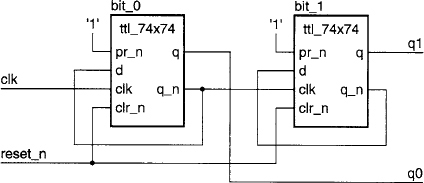


For each pair of integers that arrive on the inputs, the adder produces their sum on the output. Note that successive integers on each input may have the same value, so the adder must respond to transactions rather than to events. While integers in a pair may arrive in the inputs at different times, you may assume that neither value of the following pair will arrive until both values of the first pair have arrived. The adder should produce the sum only when both input values of a pair have arrived.

The process uses a four-phase handshaking protocol to synchronize data transfer with a consumer process. Develop a process statement to model the consumer. It, too, should use delta delays in the handshaking protocol. Include the process statements in a test-bench architecture body, and experiment with your simulator to see how it deals with models that use delta delays.
Each element of the output port is a delayed version of the input. The delay to the leftmost output element is 5 ns, to the next element is 10 ns and so on. The delay to the rightmost element is 5 ns times the length of the output port. Assume the delay line acts as an ideal transmission line.

When latch_en is asserted, data from the d input enters the latch. When latch_en is negated, the latch maintains the stored value. When out_en is asserted, data passes through to the output. When out_en is negated, the output has the value ‘Z’ (high-impedance). The propagation delay from latch_en to q is 3 ns and from d to q is 4 ns. The delay from out_en asserted to q active is 2 ns and from out_en negated to q high-impedance is 5 ns.

where the Gi are the intermediate carry generate signals, the Pi are the intermediate carry propagate signals and the Ci are the intermediate carry signals. C_1 is c_in and C3 is c_out. Your model should use the expanded equation to calculate the intermediate carries, which are then used to calculate the sums.

The arbiter should use a round-robin discipline for responding to requests. Include a concurrent assertion statement that verifies that no more than one acknowledgment is issued at once and that an acknowledgment is only issued to a requesting client.
Write a behavioral architecture body for the flipflop and a test bench that exercises the statements in the entity declaration.

The carry-look-ahead generator is connected to the four-bit adders as shown in Figure 5-35. It calculates the carry output signals using the generate, propagate and carry inputs in the same way that the four-bit counters calculate their internal carry signals.

FIGURE 5-35 Connections between a carry-look-ahead generator and adders.
is a write command, in which the bits Ai are the address and the bits Dj are the data to be written. A string of the form
is a read command, in which the bits denoted by X are ignored. The RAM produces the successive bits of read data synchronously with the last eight rising clock edges of the command.

FIGURE 5-36 Arrangement of LEDs and photodetectors on a parking lot gate.
Your model should include a clocked finite-state machine (FSM) with two inputs, one from each detector, and increment and decrement outputs that pulse to ‘1’ for one clock cycle when a car has totally entered or left the lot. The FSM outputs should drive a three-digit chain of BCD up/down counters, whose outputs are connected to seven-segment decoders.