
Throughout the previous chapters we have studiously avoided considering the case of multiple output ports connecting one signal. The problem that arises in such a case is determining the final value of the signal when multiple sources drive it. In this chapter we discuss resolved signals, the mechanism provided by VHDL for modeling such cases.
11.1 Basic Resolved Signals
If we consider a real digital system with two outputs driving one signal, we can fairly readily determine the resulting value based on some analog circuit theory. The signal is driven to some intermediate state, depending on the drive capacities of the conflicting drivers. This intermediate state may or may not represent a valid logic state. Usually we only connect outputs in a design if at most one is active at a time, and the rest are in some high-impedance state. In this case, the resulting value should be the driving value of the single active output. In addition, we include some form of “pull-up” that determines the value of the signal when all outputs are inactive.
While this simple approach is satisfactory for some models, there are other cases where we need to go further. One of the reasons for simulating a model of a design is to detect errors such as multiple simultaneously active connected outputs. In this case, we need to extend the simple approach to detect such errors. Another problem arises when we are modeling at a higher level of abstraction and are using more complex types. We need to specify what, if anything, it means to connect multiple outputs of an enumeration type together.
The approach taken by VHDL is a very general one: the language requires the designer to specify precisely what value results from connecting multiple outputs. It does this through resolved signals, which are an extension of the basic signals we have used in previous chapters. A resolved signal includes in its definition a function, called the resolution function, that is used to calculate the final signal value from the values of all of its sources.
Let us see how this works by developing an example. We can model the values driven by a tristate output using a simple extension to the predefined type bit, for example:
The extra value, ‘Z’, is used by an output to indicate that it is in the high-impedance state. Next, we need to write a function that takes a collection of values of this type, representing the values driven by a number of outputs, and return the resulting value to be applied to the connected signal. For this example, we assume that at most one driver is active (’0’ or ‘1’) at a time and that the rest are all driving ‘Z’. The difficulty with writing the function is that we should not restrict it to a fixed number of input values. We can avoid this by giving it a single parameter that is an unconstrained array of tri_state_logic values, defined by the type declaration
The declaration of the resolution function is shown in Figure 11-1. The final step to making a resolved signal is to declare the signal, as follows:
This declaration is almost identical to a normal signal declaration, but with the addition of the resolution function name before the signal type. The signal still takes on values from the type tri_state_logic, but inclusion of a function name indicates that the signal is a resolved signal, with the named function acting as the resolution function. The fact that s1 is resolved means that we are allowed to have more than one source for it in the design. (Sources include drivers within processes and output ports of components associated with the signal.) When a transaction is scheduled for the signal, the value is not applied to the signal directly. Instead, the values of all sources connected to the signal, including the new value from the transaction, are formed into an array and passed to the resolution function. The result returned by the function is then applied to the signal as its new value.
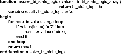
FIGURE 11-1 A resolution for resolving multiple values from tristate drivers.
Let us look at the syntax rule that describes the VHDL mechanism we have used in the above example. It is an extension of the rules for the subtype indication, which we first introduced in Chapters 2 and 4. The combined rule is

This rule shows that a subtype indication can optionally include the name of a function to be used as a resolution function. Given this new rule, we can include a resolution function name anywhere that we specify a type to be used for a signal. For example, we could write a separate subtype declaration that includes a resolution function name, defining a resolved subtype, then use this subtype to declare a number of resolved signals, as follows:
The subtype resolved_logic is a resolved subtype of tri_state_logic, with resolve_tri_state_logic acting as the resolution function. The signals s2 and s3 are resolved signals of this subtype. Where a design makes extensive use of resolved signals, it is good practice to define resolved subtypes and use them to declare the signals and ports in the design.
The resolution function for a resolved signal is also invoked to initialize the signal. At the start of a simulation, the drivers for the signal are initialized to the expression included in the signal declaration, or to the default initial value for the signal type if no initialization expression is given. The resolution function is then invoked using these driver values to determine the initial value for the signal. In this way, the signal always has a properly resolved value, right from the start of the simulation.
Let us now return to the tristate logic type we introduced earlier. In the previous example, we assumed that at most one driver is ‘0’ or ‘1’ at a time. In a more realistic model, we need to deal with the possibility of driver conflicts, in which one source drives a resolved signal with the value ‘0’ and another drives it with the value ‘1’. In some logic families, such driver conflicts cause an indeterminate signal value. We can represent this indeterminate state with a fourth value of the logic type, ‘X’, often called an unknown value. This gives us a complete and consistent multivalued logic type, which we can use to describe signal values in a design in more detail than we can using just bit values.
EXAMPLE
Figure 11-2 shows a package interface and the corresponding package body for the four-state multivalued logic type. The constant resolution_table is a lookup table used to determine the value resulting from two source contributions to a signal of the resolved logic type. The resolution function uses this table, indexing it with each element of the array passed to the function. If any source contributes ‘X’, or if there are two sources with conflicting ‘0’ and ‘1’ contributions, the result is ‘X’. If one or more sources are ‘0’ and the remainder ‘Z’, the result is ‘0’. Similarly, if one or more sources are ‘1’ and the remainder ‘Z’, the result is ‘1’. If all sources are ‘Z’, the result is ‘Z’. The lookup table is a compact way of representing this set of rules.


FIGURE 11-2 A package interface and body fora four-state multivalued and resolved logic subtype.
We can use this package in a design for a tristate buffer. The entity declaration and a behavioral architecture body are shown in Figure 11-3. The buffer drives the value ‘Z’ on its output when it is disabled. It copies the input to the output when it is enabled and the input is a proper logic level (’0’ or ‘1’). If either the input or the enable port is not a proper logic level, the buffer drives the unknown value on its output.
Figure 11-4 shows the outline of an architecture body that uses the tristate buffer. The signal selected_val is a resolved signal of the multivalued logic type. It is driven by the two buffer output ports. The resolution function for the signal is used to determine the final value of the signal whenever a new transaction is applied to either of the buffer outputs.
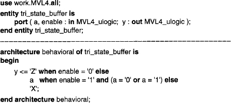
FIGURE 11-3 An entity and behavioral architecture body for a tristate buffer.

Composite Resolved Subtypes
The above examples have all shown resolved subtypes of scalar enumeration types. In fact, VHDL’s resolution mechanism is more general. We can use it to define a resolved subtype of any type that we can legally use as the type of a signal. Thus, we can define resolved integer subtypes, resolved composite subtypes and others. In the latter case, the resolution function is passed an array of composite values and must determine the final composite value to be applied to the signal.
EXAMPLE
Figure 11-5 shows a package interface and body that define a resolved array subtype. Each element of an array value of this subtype can be ‘X’, ‘0’, ‘1’ or ‘Z’. The unresolved type uword is a 32-element array of these values. The resolution function has an unconstrained array parameter consisting of elements of type uword. The function uses the lookup table to resolve corresponding elements from each of the contributing sources and produces a 32-element array result. The subtype word is the final resolved array subtype.

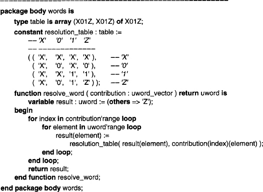
FIGURE 11-5 A package interface and body for a resolved array subtype.
We can use these types to declare array ports in entity declarations and resolved array signals with multiple sources. Figure 11-6 shows outlines of a CPU entity and a memory entity, which have bidirectional data ports of the unresolved array type. The architecture body for a computer system, also outlined in Figure 11-6, declares a signal of the resolved subtype and connects it to the data ports of the instances of the CPU and memory.


FIGURE 11-6 An outline of a CPU and memory entity with resolved array ports, and an architecture bodyfor a computer system that uses the CPU and memory.
A resolved composite subtype works well provided every source for a resolved signal of the subtype is connected to every element of the signal. For the subtype shown in the example, every source must be a 32-element array and must connect to all 32 elements of the data signal. However, in a realistic computer system, sources are not always connected in this way. For example, we may wish to connect an 8-bit-wide device to the low-order eight bits of a 32-bit-wide data bus. We might attempt to express such a connection in a component instantiation statement, as follows:
If we add this statement to the architecture body in Figure 11-6, we have two sources for elements 0 to 23 of the data signal and three for elements 24 to 31. A problem arises when resolving the signal, since we are unable to construct an array containing the contributions from the sources. For this reason, VHDL does not allow us to write such a description; it is illegal.
The solution to this problem is to describe the data signal as an array of resolved elements, rather than as a resolved array of elements. We can declare an array type whose elements are values of the MVL4_logic type, shown in Figure 11-2. The array type declaration is
This approach has the added advantage that the array type is unconstrained, so we can use it to create signals of different widths, each element of which is resolved. An important point to note, however, is that the type MVL4_logic_vector is distinct from the type MVL4_ulogic_vector, since they are defined by separate type declarations. Neither is a subtype of the other. Hence we cannot legally associate a signal of type MVL4_logic_vector with a port of type MVL4_ulogic_vector, or a signal of type MVL4_ulogic_vector with a port of type MVL4_logic_vector. One solution is to identify all ports that may need to be associated with a signal of the resolved type and to declare them to be of the resolved type. This avoids the type mismatch that would otherwise occur. We illustrate this approach in the following example. Another solution is to use type conversions in the port maps. We will discuss type conversions in association lists in Chapter 21.
EXAMPLE
Let us assume that the type MVL4_logic_vector described above has been added to the package MVL4. Figure 11-7 shows entity declarations for a ROM entity and a single in-line memory module (SIMM), using the MVL4_logic_vector type for their data ports. The data port of the SIMM is 32 bits wide, whereas the data port of the ROM is only 8 bits wide.
Figure 11-7 also shows an outline of an architecture body that uses these two entities. It declares a signal, internal_data, of the MVL4_logic_vector type, representing 32 individually resolved elements. The SIMM entity is instantiated with its data port connected to all 32 internal data elements. The ROM entity is instantiated with its data port connected to the rightmost eight elements of the internal data signal. When any of these elements is resolved, the resolution function is passed contributions from the corresponding elements of the SIMM and ROM data ports. When any of the remaining elements of the internal data signal are resolved, they have one less contribution, since they are not connected to any element of the ROM data port.

FIGURE 11-7 Entity declarations for memory modules whose data ports are arrays of resolved elements, and an outline of an architecture body that uses these entities.
Summary of Resolved Subtypes
At this point, let us summarize the important points about resolved signals and their resolution functions. Resolved signals of resolved subtypes are the only means by which we may connect a number of sources together, since we need a resolution function to determine the final value of the signal or port from the contributing values. The resolution function must take a single parameter that is a one-dimensional unconstrained array of values of the signal type, and must return a value of the signal type. The index type of the array does not matter, so long as it contains enough index values for the largest possible collection of sources connected together. For example, an array type declared as follows is inadequate if the resolved signal has five sources:
The resolution function must be a pure function; that is, it must not have any side effects. This requirement is a safety measure to ensure that the function always returns a predictable value for a given set of source values. Furthermore, since the source values may be passed in any order within the array, the function should be commutative; that is, its result should be independent of the order of the values. When the design is simulated, the resolution function is called whenever any of the resolved signal’s sources is active. The function is passed an array of all of the current source values, and the result it returns is used to update the signal value. When the design is synthesized, the resolution function specifies the way in which the synthesized hardware should combine values from multiple sources for a resolved signal.
11.2 IEEE Std_Logic_1164 Resolved Subtypes
In previous chapters we have used the IEEE standard multivalued logic package, std_logic_1164. We are now in a position to describe all of the items provided by the package, including the resolved subtypes and operators. The intent of the IEEE standard is that the multivalued logic subtypes defined in the package be used for models that must be interchanged between designers. The full package interface is included for reference in Appendix C. First, recall that the package provides the basic type std_ulogic, defined as
and an array type std_ulogic_vector, defined as
We have not mentioned it before, but the “u” in “ulogic” stands for unresolved. These types serve as the basis for the declaration of the resolved subtype std_logic, defined as follows:
The standard-logic package also declares an array type of standard-logic elements, analogous to the bit_vector type, for use in declaring array signals:
The IEEE standard recommends that models use the subtype std_logic and the type std_logic_vector instead of the unresolved types std_ulogic and std_ulogic_vector, even if a signal has only one source. The reason is that simulation vendors are expected to optimize simulation of models using the resolved subtype, but need not optimize use of the unresolved type. The disadvantage of this approach is that it prevents detection of erroneous designs in which multiple sources are inadvertently connected to a signal that should have only one source. Nevertheless, if we are to conform to the standard practice, we should use the resolved logic type. We will conform to the standard in the subsequent examples in this book.
The standard defines the resolution function resolved as shown in Figure 11-8. VHDL tools are allowed to provide built-in implementations of this function to improve performance. The function uses the constant resolution_table to resolve the driving values. If there is only one driving value, the function returns that value unchanged. If the function is passed an empty array, it returns the value ‘Z’. (The circumstances under which a resolution function may be invoked with an empty array will be covered in Chapter 16.) The value of resolution_table shows exactly what is meant by “forcing” driving values (’X’, ‘0’ and ‘1’) and “weak” driving values (’W’, ‘L’ and ‘H’). If one driver of a resolved signal drives a forcing value and another drives a weak value, the forcing value dominates. On the other hand, if both drivers drive different values with the same strength, the result is the unknown value of that strength (’X’ or ‘W’). The high-impedance value, ‘Z’, is dominated by forcing and weak values. If a “don’t care” value (’-’) is to be resolved with any other value, the result is the unknown value ‘X’. The interpretation of the “don’t care” value is that the model has not made a choice about its output state. Finally, if an “uninitialized” value (’U’) is to be resolved with any other value, the result is ‘U’, indicating that the model has not properly initialized all outputs.
In addition to this multivalued logic subtype, the package std_logic_1164 declares a number of subtypes for more restricted multivalued logic modeling. The subtype declarations are
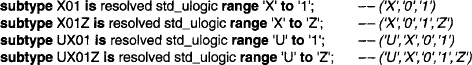

Each of these is a closed subtype; that is, the result of resolving values in each case is a value within the range of the subtype. The subtype X01Z corresponds to the type MVL4 we introduced in Figure 11-2.
The standard-logic package provides overloaded forms of the logical operators and, nand, or, nor, xor, xnor and not for standard-logic values and vectors, returning values in the range ‘U’, ‘X’, ‘0’ or ‘1’. In addition, there are functions to convert between values of the full standard-logic type, the subtypes shown above and the predefined bit and bit-vector types. These are all listed in Appendix C.
VHDL-87
The VHDL-87 version of the standard-logic package does not provide the logical operator xnor, since xnor is not defined in VHDL-87.
11.3 Resolved Signals and Ports
In the previous discussion of resolved signals, we have limited ourselves to the simple case where a number of drivers or output ports of component instances drive a signal. Any input port connected to the resolved signal gets the final resolved value as the port value when a transaction is performed. We now look in more detail at the case of ports of mode inout being connected to a resolved signal. The question to answer here is, What value is seen by the input side of such a port? Is it the value driven by the component instance or the final value of the resolved signal connected to the port? In fact, it is the latter. An inout port models a connection in which the driver contributes to the associated signal’s value, and the input side of the component senses the actual signal rather than using the driving value.
EXAMPLE
Some asynchronous bus protocols use a distributed synchronization mechanism based on a “wired-and” control signal. This is a single signal driven by each module using active-low open-collector or open-drain drivers and pulled up by the bus terminator. If a number of modules on the bus need to wait until all are ready to proceed with some operation, they use the control signal as follows. Initially, all modules drive the signal to the ‘0’ state. When each is ready to proceed, it turns off its driver (’Z’) and monitors the control signal. So long as any module is not yet ready, the signal remains at ‘0’. When all modules are ready, the bus terminator pulls the signal up to the ‘1’ state. All modules sense this change and proceed with the operation.
Figure 11-9 shows an entity declaration for a bus module that has a port of the unresolved type std_ulogic for connection to such a synchronization control signal. The architecture body for a system comprising several such modules is also outlined. The control signal is pulled up by a concurrent signal assignment statement, which acts as a source with a constant driving value of ‘H’. This is a value having a weak strength, which is overridden by any other source that drives ‘0’. It can pull the signal high only when all other sources drive ‘Z’.
Figure 11-10 shows an outline of a behavioral architecture body for the bus module. Each instance initially drives its synchronization port with ‘0’. This value is passed up through the port and used as the contribution to the resolved signal from the entity instance. When an instance is ready to proceed with its operation, it changes its driving value to ‘Z’, modeling an open-collector or open-drain driver being turned off. The process then suspends until the value seen on the synchronization port changes to ‘H’. If other instances are still driving ‘0’, their contributions dominate, and the value of the signal stays ‘0’. When all other instances eventually change their contributions to ‘Z’, the value ‘H’ contributed by the pull-up statement dominates, and the value of the signal changes to ‘H’. This value is passed back down through the ports of each instance, and the processes all resume.

FIGURE 11-9 An entity declaration for a bus module that uses a “wired-and” synchronization signal, and an architecture body that instantiates the entity, connecting the synchronization port to a resolved signal.
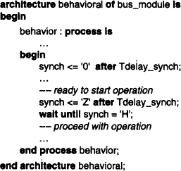
FIGURE 11-10 An outline of a behavioral architecture body for a bus module, showing use of the synchronization control port.
Resolved Ports
Just as a signal declared with a signal declaration can be of a resolved subtype, so too can a port declared in an interface list of an entity. This is consistent with all that we have said about ports appearing just like signals to an architecture body. Thus if the rchitecture body contains a number of processes that must drive a port or a number of component instances that must connect outputs to a port, the port must be resolved. The final value driven by the resolved port is determined by resolving all of the sources within the architecture body. For example, we might declare an entity with a resolved port as follows:

The architecture body corresponding to this entity might instantiate a number of I/O controller components, each with their data acknowledge ports connected to the data_ack port of the entity. Each time any of the controllers updates its data acknowledge port, the standard-logic resolution function is invoked. It determines the driving value for the data_ack port by resolving the driving values from all controllers.
If it happens that the actual signal associated with a resolved port in an enclosing architecture body is itself a resolved signal, then the signal’s resolution function will be called separately after the port’s resolution function has determined the port’s driving value. Note that the signal in the enclosing architecture body may use a different resolution function from the connected port, although in practice, most designs use the one function for resolution of all signals of a given subtype.
An extension of the above scenario is a design in which there are several levels of hierarchy, with a process nested at the deepest level generating a value to be passed out through resolved ports to a signal at the top level. At each level, a resolution function is called to determine the driving value of the port at that level. The value finally determined for the signal at the top level is called the effective value of the signal. It is passed back down the hierarchy of ports as the effective value of each in mode or inout mode port. This value is used on the input side of each port.
EXAMPLE
Figure 11-11 shows the hierarchical organization for a single-board computer system, consisting of a frame buffer for a video display, an input/output controller section, a CPU/memory section and a bus expansion block. These are all sources for the resolved data bus signal. The CPU/memory section in turn comprises a memory block and a CPU/cache block. Both of these act as sources for the data port, so it must be a resolved port. The cache has two sections, both of which act as sources for the data port of the CPU/cache block. Hence, this port must also be resolved.
Let us consider the case of one of the cache sections updating its data port. The new driving value is resolved with the current driving value from the other cache section to determine the driving value of the CPU/cache block data port. This result is then resolved with the current driving value of the memory block to determine the driving value of the CPU/memory section. Next, this driving value is resolved with the current driving values of the other top-level sections to determine the effective value of the data bus signal. The final step involves propagating this signal value back down the hierarchy for use as the effective value of each of the data ports. Thus, a module that reads the value of its data port will see the final resolved value of the data bus signal. This value is not necessarily the same as the driving value it contributes.

FIGURE 11-11 A hierarchical block diagram of a single-board computer system, showing the hierarchical connections of the resolved data bus ports to the data bus signal.
Driving Value Attribute
Since the value seen on a signal or on an inout mode port may be different from the value driven by a process, VHDL provides an attribute, ’driving_value, that allows the process to read the value it contributes to the prefix signal. For example, if a process has a driver for a resolved signal s, it may be driving s with the value ‘Z’ from a previously executed signal assignment statement, but the resolution function for s may have given it the value ‘O’. The process can refer to s’driving_value to retrieve the value ‘Z’. Note that a process can only use this attribute to determine its own contribution to a signal; it cannot directly find out another process’s contribution.
VHDL-87
The ‘driving_value attribute is not provided in VHDL-87.
11.4 Resolved Signal Parameters
Let us now return to the topic of subprograms with signal parameters and see how they behave in the presence of resolved signals. Recall that when a procedure with an out mode signal parameter is called, the procedure is passed a reference to the caller’s driver for the actual signal. Any signal assignment statements performed within the procedure body are actually performed on the caller’s driver. If the actual signal parameter is a resolved signal, the values assigned by the procedure are used to resolve the signal value. No resolution takes place within the procedure. In fact, the procedure need not be aware that the actual signal is resolved.
In the case of an in mode signal parameter to a function or procedure, a reference to the actual signal parameter is passed when the subprogram is called, and the subprogram uses the actual value of the signal. If the signal is resolved, the subprogram sees the value determined after resolution. In the case of an inout signal parameter, a procedure is passed references to both the signal and its driver, and no resolution is performed internally to the procedure.
EXAMPLE
We can encapsulate the distributed synchronization protocol described in the example on page 297 in a set of procedures, each with a single signal parameter, as shown in Figure 11-12. Suppose a process uses a resolved signal barrier of subtype std_logic to synchronize with other processes. Figure 11-13 shows how the process might use the procedures to implement the protocol.
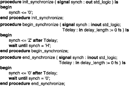
FIGURE 11-12 Three procedures that encapsulate the distributed synchronization operation.
The process has a driver for barrier, since the procedure calls associate the signal as an actual parameter with formal parameters of mode out and inout. A reference to this driver is passed to init_synchronize, which assigns the value ‘0’ on behalf of the process. This value is used in the resolution of barrier. When the process is ready to start its synchronized operation, it calls begin_synchronize, passing references to its driver for barrier and to the actual signal itself. The procedure uses the driver to assign the value ‘Z’ on behalf of the process and then waits until the actual signal changes to ‘H’. When the transaction on the driver matures, its value is resolved with other contributions from other processes and the result applied to the signal. This final value is used by the wait statement in the procedure to determine whether to resume the calling process. If the value is ‘H’, the process resumes, the procedure returns to the caller and the operation goes ahead. When the process completes the operation, it calls end_synchronize to reset barrier back to ‘0’.
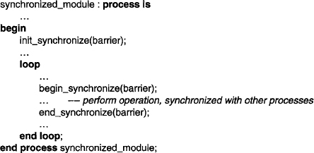
FIGURE 11-13 An outline of a process that uses the distributed synchronization protocol procedures, with a resolved control signal barrier.
Exercises
(a) ‘Z’,’1’,’Z’,’Z’?
(b) ‘O’,’Z’,’Z,’0’?
(c) ‘Z’,’1’,’Z’,’O’?
(a) “ZZZZZZZZ”, “ZZZZ0011”, “ZZZZZZZZ"?
(b) “XXXXZZZZ”, “ZZZZZZZZ”, “00000011"?
(c) “00110011”, “ZZZZZZZZ”, “ZZZZ1111"?
where MVL4_logic_vector is as described on page 292, and the following signal assignments are each executed in different processes:

What is the resolved signal value after all of the transactions have been performed?
(a) ‘Z’,’O’,’Z’,’H’?
(b) ‘H’,’Z’,’W’,’O’?
(c) ‘Z’,’W’,’L’,’H’?
(d) ‘U’,’O’,’Z’,’1’?
(e) ‘Z’,’Z’,’Z’,’-’?

FIGURE 11-14 Timing diagram for wired-and synchronization.

Tpd is the propagation delay between sensing a value on A and driving a resulting value on A. When the value on A has stabilized, it is the minimum of all request priorities. The requester with R = A wins the arbitration. If you are not convinced that the distributed minimization scheme operates as required, trace its execution for various combinations of priority values.
Each key in the keypad is a single-pole switch that shorts the row signal to the column signal when the key is pressed. Due to the mechanical construction of the switch, “switch bounce” occurs when the key is pressed. Several intermittent contacts are made between the signals over a period of up to 5 ms, before a sustained contact is made. Bounce also occurs when the key is released. Several intermittent contacts may occur over the same period before sustained release is achieved.
The keypad controller scans the keypad by setting each of the column signals to ‘0’ in turn. While a given column signal is ‘0’, the controller examines each of the row inputs. If a row input is ‘H’, the switch between the column and the row is open. If the row input is ‘0’, the switch is closed. The entire keypad is scanned once every millisecond.

FIGURE 11-16 Keypad switch connections for a touch-tone telephone.
The controller generates a set of column outputs c1_out to c3_out and a set of row outputs r1 out to r4_out. A valid switch closure is indicated by exactly one column output and exactly one row output going to ‘1’ at the same time. The controller filters out spurious switch closures due to switch bounce and ignores multiple concurrent switch closures.
Develop a package that defines a resolved type based on this scheme. Include functions for separating the bit value and strength components of a combined value, for constructing a combined value from separate bit value and strength components and for weakening the strength component of a combined value. Use the package to model a pass transistor component. Then use the pass transistor in a model of an eight-input multiplexer similar to the four-input multiplexer of Exercise 16.
Develop a high-level model of a system that uses the three-wire synchronization scheme. You should include a package to support your model. The package should include a type definition for a record containing the three synchronization wires and a pair of procedures, one to wait for a rendezvous and another to leave the rendezvous after completion of the operation. The procedures should have a bidirectional signal parameter for the three-wire record and should determine the state of the synchronization protocol from the parameter value.