

180 5. PLANAR TRANSMISSION LINES
ability of approximate analytical closed-form expressions or diagrams for the dominant mode
characteristics helps the designers of printed microwave circuits. Based on these, a microwave en-
gineer may start the design of a printed structure. e structure may then be fine tuned through
numerical electromagnetic simulation in conjunction with optimization techniques. In line with
this approach, the characteristics of the dominant quasi-TEM mode will be presented. e ap-
proximate expressions for the effective dielectric constant ."
reff
/ and the characteristic impedance
(Z
0
), by reviewing the works of Svacina [7], will be given.
Svacina, who adapted the Wheeler’s classical works [8, 9], evaluated the effective permit-
tivity ("
reff
) through a conformal transformation of a three-layer microstrip line. e remaining
dimensional relations obtained through the conformal transformation, e.g., the characteristic
impedance Z
0
, the capacitance as well as the phase and group velocities, are not affected by the
presence of the multiple layers [7]. us, their expressions (not their absolute values) remain the
same as for the single-layer case, e.g., [3].
5.3 THREE–LAYERS MICROSTRIP LINE
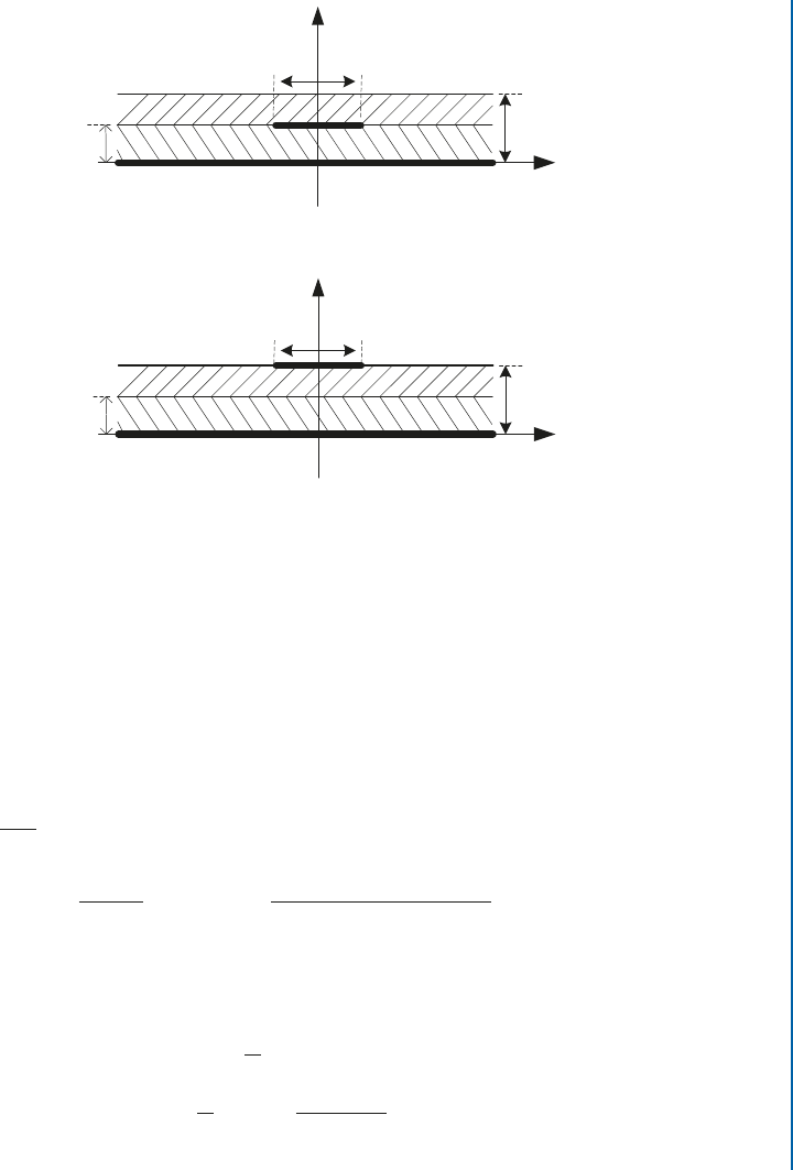
Let us now elaborate on the three-layers microstrip line studied in [9]. e strip conductor may
be located between the two dielectric layers (Figure 5.1a) or printed on the surface of the top
dielectric layer (Figure 5.1b). ese semi-infinite structures (z-plane) are first transformed to a
finite (g-plane) plane according to [9], as shown in Figure 5.2. e strip and the ground-plane
conductors are mapped to two-line segments, and the two-dielectric and air regions are mapped
to corresponding areas (S
"1
, S
"2
, S
0
) between the conductors. Each area is proportional to the
electromagnetic energy confined within the corresponding region. e filling factors .q
1
; q
2
/ of
each dielectric layer are defined in the transformed complex plane as the ratio of the area assigned
to each layer .S
"1
; S
"2
/ to the total cross-section S
c
D S
0
C S
"1
C S
"2
between the strip conduc-
tors (Figure 5.2). Recall that the filling factor represents the degree by which electromagnetic
power is confined within the corresponding layer [8, 9]. In this manner, the two filling factors
take the following form [7]:
q
1
D
S
"1
S
c
D 1
S
0
C S
"2
S
c
(5.1a)
q
2
D
S
"2
S
c
D 1
S
0
C S
"1
S
c
D 1 q
1
S
0
S
c
: (5.1b)
e filling factors are then given in [7] as follows:
5.3. THREE–LAYERS MICROSTRIP LINE 181
(a)
ε
r2
ε
r1
w
h
2
h
jy
ε
0
0
x
(b)
ε
r2
ε
r1
w
h
h
1
jy
ε
0
0
x
Figure 5.1: ree-dielectric-layers microstrip line with the strip conductor located: (a) between
the two dielectrics and (b) printed on the top dielectric layer. is is defined as the original
z-plane, .z D x C jy/.
Microstrip conductor at the dielectric interface (Figure 5.1a, Figure 5.2a)
Wide microstrips . Nw D w=h 1/:
q
1
D 1
0:5
Nw
eff
ln
Nw
eff
1
(5.2a)
q
2
D 1 q
1
0:5
1
N
U
e
Nw
eff
ln
Nw
eff
cos
0:5
N
U
e
N
h
2
0:5
C 0:5
N
U
e
C sin
0:5
N
U
e
!
; (5.2b)
where
Nw
eff
D Nw C
2
ln
Œ
17:08.0:5 Nw C 0:92/
(5.2c)
N
U
e
D
2
tan
1
2
Nw
eff
4
N
h
2
1
: (5.2d)

182 5. PLANAR TRANSMISSION LINES
(a)
S
E1
ε
r1
h
jυ
0
ε
r2
S
E2
S
0
ε
0
uu
0
(b)
S
E1
ε
r
1
h
jυ
0
u
ε
r2
S
E
2
S
0
ε
0
u
0
Figure 5.2: Conformal transformation of the three-layer microstrip line to the g-plane .g D u C
j/ where the semi-infinite cross-section is mapped to a rectangular area between two conductor
segments: (a) for Figure 5.1a and (b) for Figure 5.1b. ese are approximated according to [7].
Narrow microstrips . Nw D w= h 1/:
q
1
D 0:5
0:9
ln
.
Nw
/
(5.3a)
q
2
D 0:5 C
1
ln
.
8 Nw
/
(
0:9 C
4
ln
N
h
2
C 1
N
h
2
C 0:25 Nw 1
!
cos
1
2
4
1
1
N
h
2
C 0:125
Nw
N
h
2
s
N
h
2
C 1
N
h
2
C 0:25 Nw 1
3
5
9
=
;
: (5.3b)
e bar over each symbol represents values “normalized to h,” e.g.,
N
h
2
D h
2
=h.
With the availability of the filling factors q
1
, q
2
, the effective dielectric constant reads:
"
reff
D q
1
"
r1
C "
r2
.
1 q
1
/
2
"
r2
.
1 q
1
q
2
/
C q
2
: (5.4)

5.3. THREE–LAYERS MICROSTRIP LINE 183
Microstrip conductor printed on the top dielectric layer (Figure 5.1b, Figure 5.2b) [7]
Wide microstrips . Nw D w=h 1/:
q
1
D 0:5
N
h
1
(
1 C
4
1
Nw
eff
ln
"
Nw
eff
sin.0:5
N
h
1
/
0:5
N
h
1
C cos.0:5
N
h
1
/
#)
(5.5a)
q
2
D 1 q
1
0:5
Nw
eff
ln
Nw
eff
1
; (5.5b)
where w
eff
is given again by (5.2c).
Narrow microstrips . Nw D w= h 1/:
q
1
D ln
1 C
N
h
1
1
N
h
1
C 0:25 Nw
!
8
<
:
1 C
4
0:5 cos
1
2
4
0:125
Nw
N
h
1
s
1 C
N
h
1
1
N
h
1
C 0:25 Nw
3
5
9
=
;
=
2 ln
8
Nw
(5.6a)
q
2
D
1
2
q
1
C
0:9
ln
8
N
w
: (5.6b)
e effective dielectric constant is:
"
reff
D 1 q
1
q
2
C "
r1
"
r2
.
q
1
C q
2
/
2
"
r1
q
2
C "
r2
q
1
: (5.7)
e characteristic impedance expression remains the same as that for the single layer
microstrip line, namely [3]:
Z
0
D
Z
0;air
p
"
reff
(5.8a)
Z
0
D
120
p
"
reff
1
Nw
eff
for Nw D w= h 1 (5.8b)
Z
0
D
60
p
"
reff
ln
8
Nw
for Nw D w= h 1: (5.8c)
Equation (5.8a) is explicitly given in Section 5.12.1, but based on that, Eqs. (5.8b)
and (5.8c) are extracted. Svacina [7] tested his expressions against the numerical results [5, 6],
as well as against published results for inverted microstrips [10, 11]. Always the differences
observed were less than 2%.
..................Content has been hidden....................
You can't read the all page of ebook, please click here login for view all page.