

5.16. MICROSTRIP PRINTED ON A WEAKLY MAGNETIZED FERRITE–DIELECTRIC 215
e quantities I
1
; I
2
are the isotropic substrate dispersive models established by Schnei-
der [51] and Yamashita [52] as:
I
1
D
(
1
p
"
yy
f
f
k
2
C
1
p
"
eff 0
)
=
(
f
f
k
2
C 1
)
(5.91)
with
f
k
D
v
0
tan
1
"
req
"
eff 0
1
"
req
"
eff 0
1=2
2H
.
1 C w=H
/
"
req
"
eff 0
1=2
(5.92)
and
I
2
D
(
f
f
y
3=2
C 4
)
=
(
f
f
y
3=2
p
"
yy
C 4
p
"
eff 0
)
(5.93)
with
f
y
D
v
0
4H
p
"
req
1
n
1
2
C
1 C 2 log
1 C
w
H
2
o
: (5.94)
In the above expressions, "
req
is defined by Eq. (5.86a). H D h (mm) and the quantities
.w; h/ are those of the original line, not the equivalent ones. Also, v
0
D C is the speed
of light in vacuum. Details regarding the accuracy of (5.90) are given in [43] and the
references therein.
5.16 MICROSTRIP PRINTED ON A WEAKLY
MAGNETIZED FERRITE–DIELECTRIC SUBSTRATE
e fabrication of microstrip structures directly on a ferrite substrate (e.g., phase shifters) in-
volves numerous difficulties regarding the metallization of a ferrite surface. Printing the mi-
crostrip structure on an ordinary dielectric substrate (appropriate for microwave frequencies)
and overlaying this on top of a grounded ferrite slab as shown in Figure 5.12 constitutes a con-
venient practice [53]. Additionally, the dielectric substrates reduce the losses (decreasing the
attenuation constant) and improve the power-handling capability. However, it entails a reduc-
tion between the current wave flowing on the strip conductor and the electromagnetic fields
inside the ferrite, resulting in an undesired reduction in phase shift efficiency.
Even though the actual interest in this structure concerns the case when the ferrite is
magnetized to its saturation .M D M
S
/, herein the simpler case of its partial magnetization will
be considered in order for this structure to be handled analytically. us, the ferrite is considered
partially magnetized by a DC magnetic field aligned along the propagation axis-Oz. Hence, its
tensor permeability is given by Eqs. (5.77) and (5.79)–(5.81). From a first point of view, an
equivalent isotropic substrate approach can be employed to yield an approximate scalar relative
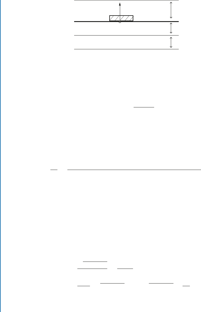
216 5. PLANAR TRANSMISSION LINES
Dielectric ε
r1
, μ
r1
Ferrite ε
r21
, μ̿
r1
→ μ
rmag
ẑ
H
DC
⊗
d
3
d
1
d
2
Figure 5.12: Microstrip line over a composite dielectric-weakly magnetized ferrite.
permeability
rmag
given by Eq. (5.82). However, Bolioli et al. [53] retained only the first term
of (5.82) as the equivalent magnetic permeability:
req
D
rT
D
2
r
k
2
r
r
: (5.95)
In turn, the same authors considered the Pucel and Masse [34] duality principle "
r
1=
rT
to establish an effective permeability. eir procedure for the composite ferrite-dielectric
substrate is illustrated in Figure 5.13, where the quasi-static effective permeability of a dual
dielectric layer (Figure 5.13a) is obtained from the related capacitances as usual:
"
reff
D
C
C
0
D
strip capacitance of dual dielectric substrate
.
d
1
; d
2
/
strip capacitance of an air substrate
.
d
1
C d
2
/
: (5.96a)
By adopting the TEM mode duality principle "
r
1=
r
as in Figure 5.13b, the 1=
reff
for a substrate with thickness d
1
C d
2
as in Figure 5.13c is:
1=
reff
D C
1
=C
0
$
reff
D C
0
=C
1
: (5.96b)
Following the Pucel and Masse [34] approach given in the previous section (see Eq. (5.48))
the propagation constant and the characteristic impedance are defined as illustrated in Fig-
ure 5.14 and given as:
Z
0
D
p
"
reff
reff
C
light
C
D
1
p
C
(5.97)
ˇ D
2f
C
light
p
"
reff
reff
D k
0
p
"
reff
reff
D
2
g
; (5.98)
where C
light
is the speed of light in free space and C the total strip capacitance for the composite
substrate.

5.16. MICROSTRIP PRINTED ON A WEAKLY MAGNETIZED FERRITE–DIELECTRIC 217
(a)
ε
d
ε
(
b)
(c)
1/μ
f
1/μ
eff
Figure 5.13: Definition of the effective permeability of a ferrite-dielectric composite, as in [53].
d
1
d
2
•
•
•
•
•
•
•
•
•
•
•
•
•
•
•
•
•
•
•
•
•
•
•
•
•
•
•
•
•
•
•
•
•
•
•
•
•
•
•
•
•
•
•
•
•
•
•
•
•
•
•
•
•
•
•
•
•
•
•
•
•
•
•
•
•
•
•
•
•
•
•
•
Dielectr
ic
Ferrite
ε
eff
, μ
eff
d
1
d
2
ε
ef
f
μ
eff
+
Figure 5.14: Definition of effective electric permittivity and effective magnetic permeability for
a ferrite-dielectric composite [53].

218 5. PLANAR TRANSMISSION LINES
Besides the above expression, following the simple approximation given in [3], the char-
acteristic impedance can be deduced as:
Z
0
.f ! 0/ D
Z
0;air
p
"
reff
reff
: (5.99)
e effective permittivity is determined according to (5.96) by ignoring the magnetic
properties of the ferrite, e.g., assuming the two layers as dielectrics with ("
0
"
rd
,
0
) and ("
rF
"
0
,
0
).
Observing Eqs. (5.97)–(5.99), the characteristic of the microstrip line can be determined
through the evaluation of capacitances C
0
, C , and C
1
. For this purpose, Bolioli et al. [53] em-
ployed a variational and a least-squares boundary residual (LSBR) method in the spectral do-
main for an electrostatic TEM approximation to estimate "
reff
and a magnetostatic TEM ap-
proximation to evaluate
reff
in closed form. e resulting expressions are as follows [53]:
Electrostatic (for "
reff
):
C D
Q
V
and V D
2
b
p
ı
X
n
X
p
K
e
n
Y
e
n
S
n;p
n ˇ
0
; (5.100)
where b is the substrate width and ı is the ratio of (strip width w)/(number of basis functions)
representing the unknown current density as shown in Figure 5.15.
K
e
n
D
1
"
0
S
n
N tanh
j
ˇ
0
n
j
d
3
N C "
r1
tanh
j
ˇ
0
n
j
d
3
"
r2
C "
r1
tanh
j
ˇ
0
n
j
d
1
tanh
j
ˇ
0
n
j
d
2
(5.101a)
N D "
r2
tanh
ˇ
ˇ
ˇ
0
n
ˇ
ˇ
d
1
C "
r1
tanh
ˇ
ˇ
ˇ
0
n
ˇ
ˇ
d
2
(5.101b)
S
n
D jnj=n and ˇ
0
D 2=b: (5.101c)
Magnetostatic (for 1=
reff
):
C
1
D
Q
V
m
and V
m
D
2
b
p
ı
X
n
X
p
K
h
n
Y
h
n
S
n;p
n ˇ
(5.102)
K
h
n
D
S
n
N tanh
.
j
ˇ
0
n
j
d
3
/
tanh
.
j
ˇ
0
n
j
d
1
/
C tanh
.
j
ˇ
0
n
j
d
3
/
N
1
C N
2
tanh
.
j
ˇ
0
n
j
d
2
/
D
1
C D
2
tanh
.
j
ˇ
0
n
j
d
3
/
; (5.103)
5.16. MICROSTRIP PRINTED ON A WEAKLY MAGNETIZED FERRITE–DIELECTRIC 219
where N; S
n
; ˇ
0
are the same as in (5.101), while additionally:
D
1
D
0
r
ˇ
ˇ
ˇ
0
n
ˇ
ˇ
2
(5.104a)
N
1
D D
1
tanh
ˇ
ˇ
ˇ
0
n
ˇ
ˇ
d
1
(5.104b)
D
2
D
0
2
r
k
2
r
ˇ
0
n
2
tanh
j
ˇ
0
n
j
.
d
1
C d
3
/
0
k
r
ˇ
0
n
ˇ
ˇ
ˇ
0
n
ˇ
ˇ
(5.104c)
N
2
D
0
2
r
k
2
r
ˇ
0
n
2
0
k
r
ˇ
0
n
ˇ
ˇ
ˇ
0
n
ˇ
ˇ
tanh
ˇ
ˇ
ˇ
0
n
ˇ
ˇ
d
1
: (5.104d)
e summation over-n concerns the discretized charge density over the strip as shown in
Figure 5.15.
ρ (y)
ΔY
ρ
i+1
Y
i+1
Y Y
i+1
w/2-w/2
y
Figure 5.15: Discretization of the charge density over the strip conductor [53].
Bolioli et al. [53] exploited the above theory for the design and implementation of phase
shifters.
(a) Application to phase shifters
e phase shifters implemented in [53] utilized an Alumina dielectric layer (Al
2
O
3
)
with "
r
D 9:6, thickness d
1
D 0:254 mm and two alternative omson/CSF ferrites of
types (A230, thickness d
2
D 1:15 mm) and (A28, thickness d
2
D 0:8 mm). Both of them
have the same dielectric constant "
r2
D 16:6, while their saturation magnetization is
4M
S
D 2300 gauss for the A230 and 4M
S
D 2800 gauss for A28. In the A230 case, the
strip width was calculated as w D 0:9 mm to give a characteristic impedance Z
0
D 50
when operated at 10 GHz. Respectively, a width of w D 0:67 mm gave Z
0
D 50 at
9 GHz for A28 case. e DC magnetic bias in both cases is created using a 2,000-turn
solenoid wrapped around the phase shifter (microstrip line) which was supplied by a vary-
ing DC-current up to 100 mA for A230 and up to 500 mA for A28, resulting in an
almost linear variation in the phase shift. Beyond this range, a nonlinear response appears
..................Content has been hidden....................
You can't read the all page of ebook, please click here login for view all page.