Chapter 3
Electronics Fundamentals
Chapter Outline
Sample and Zero-Order Hold Circuits
Logic Circuits (Combinatorial)
This chapter is for the reader who has little knowledge of electronics. It is intended to provide an overview of the subject so that discussions in later chapters about the operation and use of automotive electronics control systems will be easier to understand. The chapter discusses electronic devices and circuits having applications in electronic automotive instrumentation and control systems. Topics include semiconductor devices, analog circuits, digital circuits, and fundamentals of integrated circuits.
Semiconductor Devices
All of the active circuit devices (e.g., diodes and transistors) from which electronic circuits are built are themselves fabricated from so-called semiconductor materials. A semiconductor material in pure form is neither a good conductor nor a good insulator. The ability of a material to conduct electric current is characterized by a property called conductivity. A model for current flow in semiconductor materials and an explanation for electrical conductivity are developed later in this chapter. A metal such as copper, which is a good conductor, has a relatively high conductivity such that current flows in response to relatively low applied voltage. An insulator such as mica has a relatively low conductivity such that essentially zero current flows in response to an applied voltage. A semiconductor material has conductivity somewhere between that of a good conductor and that of a good insulator. Therefore, this material (also called semiconductor material) and devices made from it are semiconductor devices (also called solid-state devices).
There are many types of semiconductor devices, but transistors and diodes are two of the most important in automotive electronics. Furthermore, these devices are the fundamental elements used to construct nearly all modern integrated circuits. Therefore, the discussion of semiconductor devices will be centered on these two. Semiconductor devices are made primarily from silicon or germanium (although other materials, e.g., gallium arsenide, are also in use) that is purposely infused with impurities that change the conductivity of the material.
The conductivity of a pure semiconductor can be varied in a predictable manner by diffusing precisely controlled amounts of very specific impurities into it. The process of adding impurities to silicon is called “doping.” Boron and phosphorus are often used as impurity source materials to alter the conductivity of silicon. When boron is used, the semiconductor material becomes a so-called p-type semiconductor. When phosphorus is used, the semiconductor material becomes an n-type semiconductor.
In order to understand the operation of these transistors and diodes, it is helpful to understand the basic physical mechanism of electrical conductivity in both n-type and p-type semiconductor materials. The flow of an electric current through any material is due to the motion of electrons in the material in response to an applied electric field. This electric field results from the application of a voltage at the external terminals of the corresponding structure. Although the details of electric field theory are beyond the scope of this book, roughly speaking, it varies in proportion to applied voltage and inversely with the distance between the electrodes to which the voltage is applied. The electrons that move in response to this electric field originate from the individual atoms that make up the material.
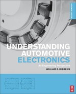
For a basic understanding of conductivity, it is helpful to refer to Figure 3.1, which depicts a relatively long, thin slab of semiconductor material across which a voltage is applied. In this figure, the electric field intensity is a vector denoted ![]() which is x directed. In this book, vectors are indicated by a bar over the symbol for the vector as exemplified by the electric field intensity
which is x directed. In this book, vectors are indicated by a bar over the symbol for the vector as exemplified by the electric field intensity ![]() . A voltage v is applied to a pair of conducting (e.g., Cu) electrodes. For this relatively long, thin semiconductor material, the magnitude of the electric field intensity E is given approximately by
. A voltage v is applied to a pair of conducting (e.g., Cu) electrodes. For this relatively long, thin semiconductor material, the magnitude of the electric field intensity E is given approximately by
![]()
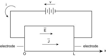
Figure 3.1 Illustration of current conduction in semiconductor.
Also shown in Figure 3.1 is the current density vector ![]() , which is also an x-directed vector. The magnitude of the current density J is the current per unit cross-sectional area and is given by
, which is also an x-directed vector. The magnitude of the current density J is the current per unit cross-sectional area and is given by
![]() (1)
(1)
where Ac is the cross-sectional area of the slab in the y, z plane. The current density vector is proportional to the electric field intensity
![]() (2)
(2)
where σ is the conductivity of the material. The reciprocal of conductivity is known as the resistivity ρ of the material:
![]() (3)
(3)
The explanation of electron flow in any material is based upon the “band theory of electrons.” This theory is a major component in modern atomic physics. According to this theory, the energy of the electrons associated with the atoms making up a material is constrained to certain ranges called bands. Any given electron will have an energy within one of these bands and no electron can have energy outside these bands. Within each band the electrons can have only discrete energy levels and only one electron can “occupy” a given energy level. Consequently, the number of electrons within each band for any atom is constrained to the number of “allowed” energy levels. An electron can only move in response to an applied electric field and contribute to current flow if there is an unoccupied energy level to which it can move as its energy changes due to the electric field intensity force acting on it.
All of the energy levels of the lower energy bands of an atom are filled such that there is no energy level to which an electron can move in response to an applied electric field. Thus, these lower band electrons cannot contribute to current flow in response to an applied voltage. The electrons in the outermost band, known as the conduction band, are the least tightly bound and for a material such as Si they are few in number relative to the number of energy levels in that band. These outer band electrons can move to an adjacent energy level and effectively move freely in response to an applied electric field. These electrons are called “free electrons.” Doping Si with phosphorus impurity results in an excess of free electrons relative to pure Si. The doped material is said to be an “n-type” semiconductor and has a conductivity that is greater than the undoped Si.
The next lowest energy band from the outer most is called the “valence band” since it is associated with the chemical valence of the material (in this case Si). The energy levels of this band are nearly (but not completely) filled. However, doping a semiconductor with a p-type impurity (e.g., doping Si with Boron) yields a relative excess of energy levels in this valence band. The resulting doped material is called a p-type semiconductor. Electrons in this band can move to the available energy levels created by doping in response to an electric field, thereby contributing to current flow. However, functionally this p-type material behaves as though it had excess of positively charged particles called “holes.” The model for current flow in a semiconductor and the explanation of semiconductor devices use the fictitious holes and their response to an applied field as a basis for the contribution they make to current flow. The terminology used to describe these charge carriers is as follows: in n-type material electrons are called “majority carriers” and holes called “minority carriers”; the reverse is true in p-type material.
Doping a semiconductor material changes the relative densities of holes and electrons. However, there is a basic relationship between these densities, which is preserved regardless of the doping concentrations. If one starts with an intrinsic semiconductor such as Si which has an equal concentration of “free” electrons and holes which are identical, we denote this concentration ni = 1.5 × 10¹⁰/cm3.
Doping Si with either a p-type or an n-type impurity changes the concentrations. Denoting electron density n, and hole density p, the following equation expresses the relationship between these concentrations under thermal equilibrium:
![]() (4)
(4)
There is another basic aspect of semiconductor physics which plays a role in the electrical characteristics of semiconductor electronic components. Whenever a voltage V is applied to a slab of semiconductor material it creates an electric field which is represented by the electric field intensity vector Ē as described above (in this text the overbar for a variable is the notation indicating that the variable is a vector).
In a semiconductor material, any electric field due to an external potential causes the electrons and holes to move with mean velocity vectors ![]() and
and ![]() , respectively. These velocities are given by
, respectively. These velocities are given by
![]()
![]()
where μe is the electron drift mobility and μh is the hole drift mobility.
These mean velocities yield electron and hole current densities ![]() and
and ![]() , respectively:
, respectively:
![]()
![]()
where q is the charge on an electron (1.6 × 10⁻¹⁹) coulomb.
These relationships will appear in models for various components in this text.
Throughout this book, current flow is taken to be conventional current in which the direction of flow is from positive to negative, whereas in reality current consists of electron motion from negative to positive. This choice of current is merely convenient for notational purposes and has no effect on the validity of any circuit analysis or design.
Diodes
A diode is a two-terminal electrical device having one electrode that is called the anode (a p-type semiconductor) and another that is called the cathode (an n-type semiconductor). A solid-state diode is formed by the junction between the anode and the cathode. In practice, a p–n junction is formed by diffusing p-type impurities on one side of the intended junction and n-type impurities on the other side.
The region in which the diode material changes from p-type to n-type material is called the p–n junction (or simply junction). The junction region is relatively short but plays a critical role in the diode operation. When the junction is formed, electrons in the vicinity of the junction migrate from the n-type to the p-type. Similarly, holes in the region migrate from p-type to n-type. This migration leaves behind a positively charged dopant ion on the n-side and a negatively charged dopant ion on the p-side over a region known as the depletion region that creates a charge distribution that in turn creates a potential difference between the two regions. In equilibrium conditions, this potential inhibits further current flow. This potential is known as the junction barrier potential since it acts more or less like a barrier to the current flow.
The current, which flows through the diode in response to an applied voltage, depends upon the polarity of the voltage as well as its magnitude. Figure 3.2 illustrates the schematic symbol for a p–n diode showing the p-type (anode) and n-type (cathode) sides of the junction. If a voltage is applied with positive on the anode and negative on the cathode, it is said to be “forward biased.” For the opposite polarity, the diode is said to be “reverse biased.” Forward bias reduces the junction barrier potential, thereby increasing current flow. Reverse bias increases that potential, thereby inhibiting current flow.

Figure 3.2 Schematic symbol (use old 3-1a). Schematic symbol for p–n diode.
The current through a forward-biased diode increases exponentially with applied voltage V, whereas the reverse-biased flow reaches a very low saturation current Is. A model for this current flow is
![]() (5)
(5)
where Is and n are parameters that are specific to a particular diode. The parameter VT is called the thermal voltage and is given by
VT = kT/q
where k is the Boltzman’s constant, T is the junction absolute temperature, and q is the electron charge.
At room temperature, ![]() . The parameter n is normally between 1 and 2 and Is is a few μ amp. Figure 3.3 depicts this current flow vs. diode junction applied voltage V. The reverse-bias current is too small to be shown.
. The parameter n is normally between 1 and 2 and Is is a few μ amp. Figure 3.3 depicts this current flow vs. diode junction applied voltage V. The reverse-bias current is too small to be shown.
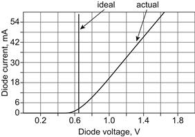
Figure 3.3 Transfer characteristic. Diode transfer characteristics.
Although the model given above for diode voltage current characteristics is a very good representation for a practical diode (provided the reverse-bias voltage is below its breakdown voltage), it is generally not necessary to represent the diode with this degree of accuracy for most circuit analysis or design purposes. Normally it is sufficient for the voltage levels involved in automotive electronics to represent a p–n diode as a polarity-dependent switch as characteristic in figures. The switch can be modeled as being open for reverse bias and closed for forward bias. With this model, the diode current in the forward bias is limited by the external circuit components to which it is connected. The reverse-bias current is taken to be zero.
Rectifier Circuit
The circuit in Figure 3.4, a very common diode circuit, is called a half-wave rectifier circuit because it effectively cuts the AC (alternating current) waveform in half in the sense that the diode passes the positive portion of the cycle and blocks the negative portion of the cycle.
Figure 3.4 Rectifier circuit.
Consider the circuit first without the dotted-in capacitor. The alternating current voltage source is assumed to be a sine wave with a peak-to-peak amplitude of 100 V (50-V positive swing and 50-V negative swing). Waveforms of the input voltage and output voltage plotted against time are shown as the solid lines in Figure 3.5. Notice that the output never drops below 0 V. The diode is reverse biased and blocks current flow when the input voltage is negative, but when the input voltage is positive, the diode is forward biased and permits current flow. If the diode direction is reversed in the circuit, current flow will be permitted when the input voltage is negative and blocked when the input voltage is positive. Rectifier circuits are commonly used to convert the AC voltage into a DC voltage (e.g., for use with automotive alternators to provide DC current battery charging and to supply electrical power to the vehicle). Using a capacitor to store charge and resist voltage changes smoothes the rippling or pulsating output of a half-wave rectifier.
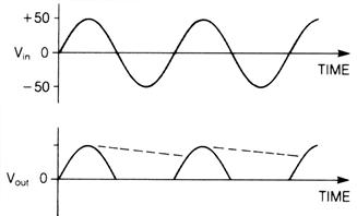
Figure 3.5 Rectifier waveforms.
The input voltage Vin of Figure 3.4 is AC; the output voltage Vout has a DC component and a time-varying component, as shown in Figure 3.5.
The output voltage of the half-wave rectifier can be smoothed by adding a capacitor, which is represented by the dotted lines in Figure 3.4. The combination of the load resistance (R) and the capacitor (C) forms a low-pass filter, which acts to smooth the fluctuating output of the half-wave rectifier diode. Since the capacitor stores a charge and opposes voltage changes, it discharges (supplies current) to the load resistance R when Vin is going negative from its peak voltage. The capacitor is recharged when Vin comes back to its positive peak and current is supplied to the load by the Vin. The result is Vout that is more nearly a smooth, steady dc voltage, as shown by the dotted lines between the peaks of Figure 3.5. The amplitude of the ripples in the output voltage can be made insignificant by choosing a capacitor having sufficiently large capacitance, which lowers the low-pass filter corner frequency and attenuates the ripple components (see Chapter 1).
There are many diode applications including some in communications systems. Often, it is desirable to change the carrier frequency of an information-carrying signal. The highly nonlinear transfer characteristics of a diode make it an excellent component for a process known as “frequency mixing.” Whenever two or more signals are passed through a diode, a signal is generated that includes components whose frequencies are the sum and the difference of the two original signal frequencies. Figure 3.6 depicts a simplified embodiment of the frequency-mixing concept.
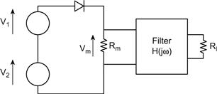
Figure 3.6 Frequency “mixing” circuit.
Let the two voltage sources have terminal voltages v1, v2: where ![]() :
:
![]()
It can be shown that the voltage across Rm is given by
 (6)
(6)
where the coefficients Cm,n are functions of V1,V2 as well as Rm and m, n are integers. The amplitudes of these coefficients are largest for relatively small n and m and asymptotically approach 0 as ![]() and
and ![]() . In most communications, application frequency mixing circuits are used to select the desired frequency components. The filter pass band encloses the desired frequency component and its stop bands reject the unwanted frequency components (see Chapter 1).
. In most communications, application frequency mixing circuits are used to select the desired frequency components. The filter pass band encloses the desired frequency component and its stop bands reject the unwanted frequency components (see Chapter 1).
Transistors
Diodes are static circuit elements; that is, they do not have gain or store energy. Transistors are active elements because they can amplify or transform a signal level. Transistors are three-terminal circuit elements that act like voltage or current-controlled current amplifiers. Transistors come in two major categories that are termed “bipolar” or “field effect” depending upon whether they are current or voltage controlled, respectively. There are two common bipolar (i.e., consisting of n-type and p-type semiconductors) types denoted 1) NPN and 2) PNP.
Physically, an NPN transistor structure consists of a thin p-type material (called BASE) sandwiched between 2 n-type pieces, which are called the COLLECTOR and the EMITTER. A PNP transistor has a thin n-type material as the BASE between a p-type EMITTER and p-type COLLECTOR.
Bipolar transistors can be made to amplify or switch in three different circuit configurations: 1) grounded emitter, 2) grounded base, and 3) grounded collector. For the present discussion, we will use Figure 3.7a and b to depict the schematic symbols for both bipolar types. The direction of conventional current flow for each of the terminals for collector (Ic), emitter (Ie), and base (Ib) is shown in these schematic symbol drawings. Figure 3.8 depicts a circuit configuration for a grounded emitter NPN amplifier whose theory of operation is explained later in this chapter.

Figure 3.7 Transistor schematic symbols.

Figure 3.8 NPN transistor amplifier circuit.
The signal being amplified is represented by source voltage vs and source resistance Rs. The load resistance R![]() connects the collector to the positive DC power supply voltage Vcc. The output, amplified signal is taken at the collector–R
connects the collector to the positive DC power supply voltage Vcc. The output, amplified signal is taken at the collector–R![]() junction and is denoted vo. For linear amplification, a bias resistance Rb supplies a DC current to the base. The purpose of the bias current is explained later with respect to the operation of a transistor as an amplifier.
junction and is denoted vo. For linear amplification, a bias resistance Rb supplies a DC current to the base. The purpose of the bias current is explained later with respect to the operation of a transistor as an amplifier.
Transistors are useful as amplifying devices. During normal operation, current flows from the base to the emitter in an NPN transistor. The collector–base junction is reverse biased, so that only a very small amount of current flows between the collector and the base when there is no base current flow.
The base–emitter junction of a transistor acts like a diode. Under normal operation for an NPN transistor, current flows forward into the base and out the emitter, but does not flow in the reverse direction from emitter to base. The arrow on the emitter of the transistor schematic symbol indicates the forward direction of current flow. The collector–base junction also acts as a diode, but supply voltage is always applied to it in the reverse direction. This junction does have some reverse current flow, but it is so small (10−6 to 10−12 amp) that it is ignored except when operated under extreme conditions, particularly temperature extremes. In some automotive applications, the extreme temperatures may significantly affect transistor operation. For such applications, the circuit may include components that automatically compensate for changes in transistor operation.
The operation of an NPN bipolar junction transistor (BJT) in grounded emitter configuration can be understood with reference to Figure 3.9. In this configuration, the individual component regions – collector, base, and emitter – are depicted along with the very important depletion regions in each at both junctions. Voltages Vce and Vbe are the voltages of the collector (+) and the base (+) relative to emitter (ground), where Vce > Vbe. These voltages reverse bias the collector–base junction and forward bias the base–emitter junction. The electrically neutral portions of the collector and emitter are denoted n and the neutral portion of the base is denoted p. The reverse-bias collector–base voltage is denoted Vcb and is given by
![]()
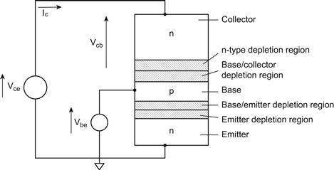
Figure 3.9 NPN grounded emitter configuration and voltages.
An increase in Vce (without changing Vbe) increases the reverse bias which increases the depletion region in both the collector and base. There is no change in the depletion region of the emitter–base junction (for fixed Vbc). Consequently, the neutral base region is decreased in size along the active path between collector and emitter.
The narrowing of the base reduces the probability of any recombination of a charge carrier with an impurity ion. In addition, the gradient of the charge density across the base is increased such that the current, due to minority carriers injected across the base–emitter junction, increases. The result of these effects is to increase the collector (i.e., output) current as Vce is increased.
The operating characteristics for a bipolar transistor are given as a set of curves of Ic(Vce,Vbe) known as characteristics curves. The characteristic curves for a typical small signal NPN transistor (i.e., 2N4401) in the grounded emitter configuration are given in Figure 3.10. These curves are parametrized in terms of base current (in μ amp). Note that each curve for a fixed Vbe increases from Ic = 0 at Vce = 0, reaching a saturation value and beyond this point increases roughly linearly, with VCE. A large signal model for the grounded emitter bipolar transistor is given by the so-called Early model:
![]() (7)
(7)
![]()
![]()
where Is is the saturation current for the reverse-biased collector-base junction, VT is the thermal voltage = kT/q, VA is the so-called Early voltage (in the approximate range 15–150 V), and βF0 is the forward common emitter current gain at zero bias:
![]()
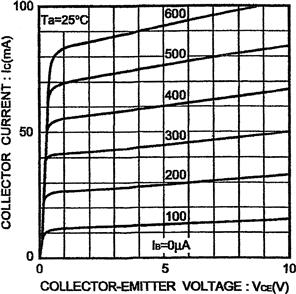
Figure 3.10 Grounded emitter output characteristics.
A small signal linear model for the transistor is given in Figure 3.11. This model is the most useful for performance analysis/design of linear modes of operation.
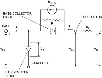
Figure 3.11 Current and voltages for NPN transistor.
In this model, the collector current is modeled by a current-controlled current source (hfeIb) shunted by a resistance R (source impedance). The base current Ib is determined by the source being amplified along with external circuit impedances.
The base–emitter diode does not conduct (there is no transistor base current) until the voltage across it exceeds Vd volts in the forward direction. If the transistor is a silicon transistor, Vd equals 0.7 V just as with the silicon diode. The collector current Ic is zero until the base–emitter voltage Vbe exceeds 0.7 V. This is called the cutoff condition, or the off condition, when the transistor is used as a switch.
When Vbe rises above 0.7 V, the diode conducts and allows some base current Ib to flow. Figure 3.10 shows that the transistor voltage/current characteristics, though basically nonlinear, have a linear region of operation. A variation in base current about a point such as ![]() produces a variation in collector current that is highly linear. The so-called common emitter forward current gain, denoted hfe, is given by
produces a variation in collector current that is highly linear. The so-called common emitter forward current gain, denoted hfe, is given by
![]() (8)
(8)
It is common practice in linear transistor circuit analysis/design to denote d-c components of voltage/current with uppercase letters and variations about these d-c values with lowercase letters. For example, collector current can be modeled as
![]() (9)
(9)
Similarly, the base current Ib can be modeled as given below
![]() (10)
(10)
At any d-c base current (that is called the base bias current) and is denoted Io in Figure 3.11 the collector a-c current ic is given by
![]() (11)
(11)
The current gain (hfe) can range from 10 to 200 depending on the transistor type, but is nearly constant over a large range of Vce, Ib, Ic. The collector current is represented by a current generator in the collector circuit of the model in Figure 3.11. This condition is called the active region because the transistor is conducting current and amplifying. It is also called the linear region because collector current is (approximately) linearly proportional to base current. The dotted resistance in parallel with the collector–base diode represents the leakage of the reverse-biased junction, which is normally neglected, as discussed previously.
A third condition, known as the saturation condition, exists under certain conditions of collector–emitter voltage and collector current. In the saturation condition, large increases in the transistor base current produce little increase in collector current. When saturated, the voltage drop across the collector–emitter is very small, usually less than 0.5 V. This is the “on” condition for a transistor switching circuit. This condition occurs in a switching circuit when the collector of the transistor is tied through a resistor RL to a supply voltage Vcc as shown in Figure 3.8. In this mode of operation, the source voltage is large enough that the base current drives the transistor into the saturated condition, in which the output voltage (voltage drop from collector to emitter) is very small and the collector–base diode may become forward biased.
Having briefly described the behavior of transistors, it is now possible to discuss circuit applications for them. As an example of the use of this small signal model, consider the analysis of the simple amplifier circuit of Figure 3.12a. In this figure, a signal represented by the a-c voltage vs and source resistance Rs, and capacitor C is amplified to an output signal vo. The purpose of adding the capacitor is to block the d-c base current through the bias resistor Rb from flowing through the source. This output voltage is produced by collector variation (due to source voltage variations) acting through load resistance RL.

Figure 3.12 Grounded emitter NPN transistor amplifier.
In a transistor amplifier, a small change in base current results in a corresponding larger change in collector current. In order to achieve linear amplification the transistor is biased with a d-c current Io via bias resistor Rb. The characteristic curves for this transistor are shown in Figure 3.11b. The straight line (called the load line) connecting Vce = Vcc with Ic = Ics represents the variation in voltage Vo and collector current Ic with variation in base current due to signal voltage Vs. The slope of the load line SLL is given by
![]() (12)
(12)
![]()
![]()
With vs = 0, the bias current is given by
![]() (13)
(13)
where Vd is the forward-bias voltage drop across the base–emitter junction, which is typically negligible in comparison with Vcc. The analysis of this circuit is done using the small signal model of Figure 3.12c in which the load resistance at terminal Vcc is at a-c ground potential. The output voltage vo of circuit in Figure 3.12a is the a-c component of Vce.
This model, which is often termed the “small signal linear incremental transistor model,” is actually an idealized (fictional) equivalent circuit that is only valid for linear amplification and represents only the time varying (i.e., a-c) components of voltages and currents. In this model, the collector current ic is represented by a current-controlled ideal current source shunted by a source resistance Rc. An ideal current source is an artificial circuit component that produces a current that is independent of any load impedance. The current generated is proportional to base current ib and is given by
![]() (14)
(14)
Assuming Rc >> RL (which is the usual case), the output voltage vo is given by
![]() (15)
(15)
![]() (16)
(16)
Note that the collector voltage and base current are 180° out of phase. This phase change occurs because load resistance end that is physically connected to the power supply (i.e., Vcc) is at a-c ground potential and the a-c collector current flows in the direction shown in Figure 3.12c. The base circuit analysis is conducted by summing the voltage components around the base circuit loop
![]() (17)
(17)
The capacitor voltage vc is given by
 (18)
(18)
Eqn (17) can be solved for base current ib by using the Laplace transform method of Chapter 1 yielding the following Equation for ib(s):

![]() (19)
(19)
Substituting ib(s) from Eqn (19) into Eqn (16) yields the transistor circuit voltage gain G:
 (20)
(20)
![]()
![]() (21)
(21)
The dimension of the product RsC is time such that ωo has the dimension of frequency (in rad/s).
The variation of gain with input frequency can be determined from the steady-state sinusoidal frequency response for the gain [G(jω)]. In Chapter 1, it was shown that the sinusoidal frequency response of any system is found by replacing s with jω in the operational transfer function. Thus, the frequency dependence of amplifier gain is given by
![]() (22)
(22)
For frequencies ω >> ωo, the amplifier gain approaches a constant value
![]() (23)
(23)
that is, the circuit of Figure 3.12a is a “high pass” amplifier. The d-c blocking capacitor C is chosen during circuit design such that ωo is smaller than the lowest component in vs.
In practice, transistor amplifiers frequently consist of multiple stages of the form of Figure 3.12a connected in cascade, each with a capacitor coupling its output to the input of the next stage. Of course, the time domain output can be found by taking the inverse Laplace transform of vo(s) as shown in Chapter 1.
In addition to the linear region of operation, a transistor can be made to operate nonlinearly as a switch as explained above with respect to saturation and cutoff regions. For this application, the bias resistor is omitted. Circuit parameters and input voltages are chosen such that the transistor switches abruptly from cutoff in which ![]() and saturation in which Ic = Icsat. This type of operation is used in digital circuits, which are discussed later in this chapter. As will be shown later, both input and output voltages are binary valued.
and saturation in which Ic = Icsat. This type of operation is used in digital circuits, which are discussed later in this chapter. As will be shown later, both input and output voltages are binary valued.
Field-Effect Transistors
The types of transistors discussed above are known as bipolar transistors because they operate by conduction via both electrons and holes. As explained earlier, they amplify relatively weak base currents yielding relatively large collector–emitter output currents. They are in effect current-controlled current amplifiers. Another type of transistor operates as a voltage-controlled amplifier and is called a field-effect transistor (FET). There are many variations of FETs, as explained below.
Unlike the bipolar transistor, which is fabricated with two p–n junctions, the field-effect transistor consists of a slab of either n-type or p-type semiconductor to which electrodes are bonded as depicted in Figure 3.13. An FET is known as either an n-channel or a p-channel FET depending upon whether the semiconductor is n-type or p-type material, respectively.
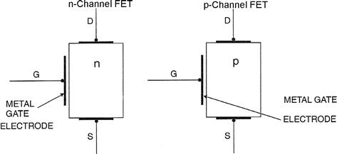
Figure 3.13 Field-effect transistor configuration.
An FET is a three-terminal active circuit element having a pair of electrodes connected at opposite ends of the slab of semiconductor and called source (denoted S) and drain (denoted D). A third electrode, called the gate (denoted G), consists of a thin layer of conductor that is electrically insulated from the semiconductor slab.
There are many types of FETs characterized by fabrication technology, material doping (i.e., n-channel or p-channel), and whether the gate voltage tends to increase the number of charge carriers (called enhancement mode) or decrease the number of charge carriers (depletion mode). The FET circuit schematic symbols for n-type and p-type enhancement modes are shown in Figure 3.14.
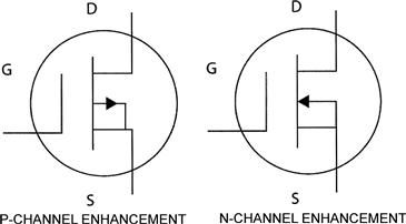
Figure 3.14 Circuit symbol for FET transistors.
Perhaps the most common gate fabrication involves a metal with an oxide layer placed against the semiconductor in the sequence metal-oxide semiconductor (MOS). The oxide layer insulates the metal electrode from the semiconductor so that no current flows through the gate electrode. Rather, the voltage applied to the gate creates an electric field that controls current flow from source to drain. The terminology for an FET having this type of gate structure is NMOS or PMOS, depending on whether the FET is n-channel or p-channel. Often, circuits are fabricated using both in a complementary manner, and the fabrication technology is known as complementary-metal-oxide semiconductor (CMOS). Regardless of the fabrication technology or the type of semiconductor, FET functions as a voltage-controlled current source.
The analysis procedure for all FET-type transistors is essentially the same as for a bipolar transistor. An example-amplifying circuit, shown in Figure 3.15, depicts the current path from power supply VDD through a load resistor RL and through the transistor from D to S and then to ground using an n-channel enhancement mode FET. A signal voltage vs applied at the gate electrode controls the current flow through the FET and thereby through the load resistance RL. Functionally, the FET operates like a voltage-controlled current source. A relatively weak signal applied to the gate can yield a relatively large voltage Vo across the load resistance.
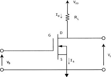
Figure 3.15 Simple FET amplifier.
We illustrate such analysis with an example based upon Figure 3.12c. The small signal (a-c) equivalent circuit model for this circuit is shown in Figure 3.16.
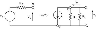
Figure 3.16 Small signal circuit model for FET amplifier.
The input impedance for an FET is sufficiently large that the gate voltage is approximately the source voltage ![]() . The equivalent circuit of Figure 3.16 includes a voltage-controlled current source whose output current is controlled by gate voltage vG. This current source is shunted by source resistance R. In this case, the voltage-controlled current source with current
. The equivalent circuit of Figure 3.16 includes a voltage-controlled current source whose output current is controlled by gate voltage vG. This current source is shunted by source resistance R. In this case, the voltage-controlled current source with current
![]()
where ![]()
The parameter gm is called the “transconductance” for the FET. The output voltage vo is given by
![]()
![]() (24)
(24)
Note that the FET amplifier produces a 180° phase shift from vs to vo similar to the bipolar amplifier.
The above example illustrates the analysis procedures for any FET. Of course, any given FET amplifier circuit may incorporate frequency-dependent components (e.g., inductors and capacitors), which requires analysis via transform techniques as explained in Chapter 1 and similar to that used in the bipolar transistor analysis.
Integrated Circuits
In modern automotive electronic systems/subsystems, transistors only seldom appear as individual components (except for relatively high-power applications as drivers for fuel injection or spark generation). Rather, multiple transistors (numbering in the tens of thousands are created on a single Si chip). This is particularly true of digital circuits which are discussed later in this chapter. These combined circuits are termed integrated circuits and are packaged with dozens or hundreds of leads configured such that they can be attached via soldered connections to a so-called printed circuit board. A printed circuit consists of a thin insulating board onto which conductors are formed that provides the interconnection between multiple integrated circuits to form an electronic system/subsystem.
Analog filtering or other signal processing has largely disappeared from contemporary automobiles. However, some older vehicles may still be on the road in which there is some analog signal processing. Moreover, analog signal processing is sometimes combined with an analog sensor. For the sake of completeness, a brief discussion of analog signal processing is included here. Analog filtering/signal processing is, perhaps, best illustrated with integrated circuits called “operational amplifiers.”
Operational Amplifiers
An operational amplifier (op amp) is an example of a standard building block of integrated circuits and has many applications in analog electronic systems. It is normally connected in a circuit with external circuit elements (e.g., resistors and capacitors) that determine its operation. An op amp is a differential amplifier which typically has a very high voltage gain of 10,000 or more and has two inputs and one output (with respect to ground), as shown in Figure 3.17a. A signal applied to the inverting input (–) is amplified and inverted (i.e. has polarity reversal) at the output. A signal applied to the noninverting input (+) is amplified, but it is not inverted at the output.
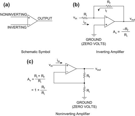
Figure 3.17 Op amp circuits.
Use of Feedback in Op Amps
The op amp is normally not operated at maximum gain, but feedback techniques can be used to adjust the closed-loop gain and dynamic response to the value desired, as shown in Figure 3.17b. The output is connected to the inverting input through circuit elements (resistors, capacitors, etc.) which determine the closed-loop gain.
The output voltage vout for an op amp having no feedback path (i.e., open loop) is given by
![]() (25)
(25)
where v1 is the noninverting input voltage, and v2 is the inverting input voltage.
Alternatively, this equation can be rewritten in a form from which the relationships between the inverting and noninverting inputs can be found for an ideal op amp (having open-loop gain A → ∞):
![]()
Thus, the 2 input voltages will approach identity for a high-quality (i.e., high A) op amp as represented by the following condition:
![]()
The internal resistance between the inverting and non-inverting inputs is denoted Rin and is relatively large compared to external resistances used in normal up-amp applications. In the example of Figure 3.17b, the feedback path consists of resistor Rf. The gain is adjusted by the ratio of the two resistors and is calculated by the following analysis. For this circuit configuration, the noninverting for which we can write
![]()
In order that v1 = 0, the currents at the inverting input must sum to zero:
![]()
![]()
![]()
![]()
![]()
![]()
The closed-loop gain ![]() is defined
is defined
 (26)
(26)
The phase change of 180° between vin and vout is indicated by the negative Ac![]() .
.
The op amp can readily be configured to implement a low-pass filter using the circuit depicted in Figure 3.18. The components in the feedback path include the parallel combination of resistor Rf and capacitor C. In this circuit, as in any other inverting mode circuit with the noninverting mode grounded, the currents into the inverting input sum to 0. Using the Laplace transform methods of Chapter 1 and the model for capacitor voltage/current relationships (i.e., ![]() ), the model for the inverting mode currents is given below:
), the model for the inverting mode currents is given below:
![]() (27)
(27)

Figure 3.18 Low-pass filter op amp circuit.
Solving for vo/vs gives the closed-loop gain ![]() (as a transfer function):
(as a transfer function):
 (28)
(28)
With reference to the discussion in Chapter 1 on continuous time systems, it can be seen that steady-state sinusoidal frequency response ![]() is a low-pass filter having corner frequency ωc = 1/RfC:
is a low-pass filter having corner frequency ωc = 1/RfC:
![]() (29)
(29)
The minus sign in the equation means signal phase inversion from input to output. Moreover, the closed-loop gain is independent of the open-loop gain (as long as A is large). Furthermore, since both the inverting and noninverting inputs are held at ground potential, the input impedance of the op amp circuit of Figure 3.17b presented to input voltage vin is the resistance of Ri.
A noninverting amplifier is also possible, as shown in Figure 3.17c. The input signal is connected to the noninverting (+) terminal, and the output is connected through a series connection of resistors to the inverting (–) input terminal. The voltage gain, Av, in this case is
![]() (30)
(30)
Note that this noninverting circuit has no phase inversion from input to output voltage. The minimum closed-loop gain for this noninverting amplifier configuration (with Rf = 0) is unity. Besides adjusting gain (via the choice of Rf and Ri), negative feedback also can help to correct for the amplifier’s nonlinear operation and distortion. The input impedance presented to the input voltage vin by the noninverting op amp configuration of Figure 3.17c is very large (ideally infinite). This high input impedance is one of the primary features of the noninverting op amp configuration.
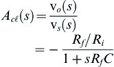
Summing Mode Amplifier
One of the important op amp applications is summing of voltages. Figure 3.19 is a schematic drawing of a summing mode op amp circuit.
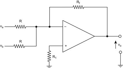
Figure 3.19 Schematic drawing of a summing mode op amp circuit.
In this circuit, a pair of voltages va and vb (relative to ground) is connected through identical resistances R to the inverting input. Using the property of inverting mode op amps that the currents into the inverting input sum to 0, it can be shown that the output voltage vo is proportional to the sum of the input voltages:
![]() (31)
(31)
Phase-Locked Loop
Another example of analog integrated circuit signal processing having automotive application is a device known as a “phase-locked loop” (PLL). This circuit can be used with certain analog (continuous time) sensors to provide an analog signal that can be further processed by a digital electronic system after it is sampled. The PLL finds application in the demodulation of phase- or frequency-modulated signals. At least one automotive application is the measurement of instantaneous crankshaft angular speed as explained later in this book.
A block diagram for the PLL circuit is shown in Figure 3.20.
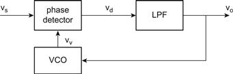
Figure 3.20 Block diagram for PLL.
In this figure, the input signal vs(t) is assumed to be phase ![]() modulated and is given by
modulated and is given by
![]() (32)
(32)
where ![]() is the instantaneous phase modulation.
is the instantaneous phase modulation.
A corresponding frequency-modulated signal has instantaneous frequency given by
![]()
where Ωs is the time average frequency and δωs is the frequency deviation from mean (i.e., modulation).
In any practical application of the PLL for automotive systems, the modulation deviation is a small fraction of the carrier frequency (i.e., ![]() ).
).
The other components in Figure 3.20 include a phase detector, a low-pass filter (LPF), and a voltage-controlled oscillator (VCO). The phase detector is functionally an electronic multiplier that generates an output voltage vd given by
![]() (33)
(33)
where Kd is the constant for the device.
The VCO is an oscillator having an output voltage vv(t) whose instantaneous frequency (ωv(t)) is controlled by voltage vo (from the LPF) such that
![]() (34)
(34)
where
 (35)
(35)
![]() (36)
(36)
where Kv is the constant for the VCO circuit.
The PLL circuit is an electronic closed-loop control system (see Chapter 1). After a brief transient period during which the VCO frequency is controlled, its frequency is “locked” to ωs (i.e., ωv(t) = ωs(t)) provided Ωs is within the so-called “capture range” for the VCO. That is, PLL lock occurs provided
![]() (37)
(37)
![]() (38)
(38)
For frequency modulation cases, under lock conditions the VCO voltage is given by
![]() (39)
(39)
where ωv = ωs.
The instantaneous phase difference ![]() is linearity proportional to the frequency deviation δωs from the mean frequency Ωs:
is linearity proportional to the frequency deviation δωs from the mean frequency Ωs:
![]() (40)
(40)
where ![]() is a constant for the VCO.
is a constant for the VCO.
The phase detector output voltage is given by
![]() (41)
(41)
![]() (42)
(42)
The LPF suppresses the term at frequency 2ωs and for small modulation ![]() such that the output voltage
such that the output voltage
![]() (43)
(43)
That is, the LPF output signal is proportional to the frequency modulation. Thus, this circuit is an FM demodulator. The filter pass band must be sufficiently large to accommodate the spectrum of δωs.
Sample and Zero-Order Hold Circuits
Chapter 2 introduced the concept of ideal sample and zero-order hold circuit, which is used in discrete time digital systems. In order to understand the implementation of digital electronics in automotive systems, it is, perhaps, worthwhile to discuss, briefly, some actual circuit configurations for practical realizations of these important system components.
Recall from Chapter 2 that the input (xk) to a digital system is essentially a numerical representation in binary or binary-coded format of a sample of a continuous time voltage variable v(t) at sample time tk:
![]() (44)
(44)
where NB signifies an N-bit binary representation of V(tk) (i.e., see Chapter 4). This sampling process involves two steps: 1) obtaining a voltage sample at tk and 2) converting this sample to the N-bit numerical format. The first step can be accomplished, in theory, via a switch that connects the continuous time voltage to a low-loss capacitor for a sufficient duration to charge the capacitor to the voltage value v(tk).
Figure 3.21 depicts a sampler for a digital system that works in conjunction with an A/D converter as described above. The A/D converter is explained in detail with example circuits in Chapter 4. This figure depicts the equivalent circuit of the source being sampled including its source impedance (assumed to be resistive) Rs as well as a very low leakage capacitor C. The capacitor maintains voltage v(tk) sufficiently long to permit the A/D to complete its conversion. In Figure 3.21a, the switch S model is
![]() (45)
(45)
![]()
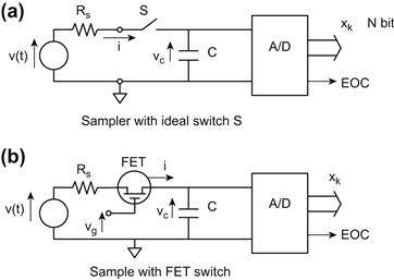
Figure 3.21 Sample circuit.
The duration of the switch closure τs must be long enough for the A/D conversion to be complete at which time an output EOC = 1 (logical) indicating “end of conversion” to the digital system. It is assumed for convenience that the input impedance of the A/D converter is sufficiently large that its input current is negligible.
During the period in which the switch is closed (at sample time tk), the source voltage supplies current to the capacitor to change its voltage from vc = v(tk−1) to vc = v(tk). The model for this circuit is given by
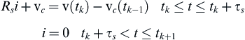 (46)
(46)
where ![]() ; q is the charge on capacitor, and where
; q is the charge on capacitor, and where ![]() ; C is the capacitance of capacitor:
; C is the capacitance of capacitor:
![]()
Eqn (24) can readily be rewritten in terms of vc:
![]() (47)
(47)
![]()
![]()
where vck is ideally held constant by the capacitor until time tk+1. Because the output voltage of the above circuit “holds” the sample of source voltage vck for the indicated period, it is usually called a “sample and hold” circuit. The solution to the first-order differential Eqn (25) is readily obtained using the Laplace transform method given in Chapter 1:
![]() (48)
(48)
![]()
where τ = RsC.
Ideally, the capacitor voltage vck should equal the sampled value of the source voltage v at t = tk. This ideal voltage is approximated by the actual voltage vck provided τ << τs. Furthermore, τs should be small compared to the time that the source changes such that
![]()
In order for this latter condition to be achieved, the sample duration period τs and the system sample period T must both be small. It was shown in Chapter 2 that the sample frequency Fs = 1/T must be greater than twice the highest frequency in v(t) to avoid aliasing errors. Furthermore, the sample duration must be larger than τ (i.e., τs >> τ) in order for the sampler to approximate the ideal sampler performance. This latter objective requires that the capacitance C satisfies the following inequality:
![]()
In the practical sample circuit of Figure 3.21b, the switch function is implemented via an FET whose source to drain resistance (RSD) is a function of a control voltage vg applied to the gate of the transistor. The switching operation can be achieved a control voltage by a periodic pulse train form as given by
![]() (49)
(49)
![]()
With vg(t) above applied to the FET gate, the source/drain resistance is given by
![]()
![]()
Ideally, these resistances should be
![]()
![]()
However, in practice, Roff is finite, but large, and Ron is small, but nonzero. Provided Roff is sufficiently large, the model for the circuit of Figure 3.21 is given by
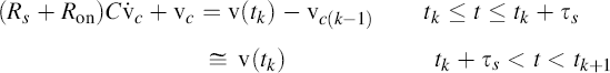 (50)
(50)
The circuit in which the switch is implemented by the FET has the same dynamic response as that of the ideal switch model except that the time constant τ is given by
![]()
The performance of the practical sample circuit can approach that of the ideal sample by proper choice of circuit and system parameters.
Zero-order hold circuit
In addition to the ideal sampler component introduced in Chapter 2, the ideal ZOH component was shown to be required whenever a digital system output must be converted to an analog electrical signal (e.g., to operate an analog actuator). The ZOH circuit is similar in certain respects to the “sample and hold” circuit introduced above, in that it is synchronous with the sampler at the system input and that it must hold a voltage between successive sample times. In addition, it incorporates a low-leakage capacitor to “hold” the voltage.
Figure 3.22 depicts a ZOH circuit in which the system input yk is the kth digital system output. In the figure, the digital system (not shown) generates an output sequence {yk} in the form of an N-bit binary “word” on a set of N-leads that are connected to the D/A converter. The D/A converter is explained in detail (along with the schematic diagrams) in Chapter 4. The digital control system also generates a signal that controls the D/A operation such that, at the end of the conversion (EOC), the D/A output analog voltage ![]() corresponds to the numerical value of yk. The EOC output triggers a pulse generator having output voltage vg(t) given by
corresponds to the numerical value of yk. The EOC output triggers a pulse generator having output voltage vg(t) given by
![]() (51)
(51)
![]()

Figure 3.22 ZOH circuit.
The pulse duration τs must be sufficiently long that the capacitor voltage is approximately (ideally) ![]() . Voltage vg is applied to the FET gate, which functions as a voltage-controlled switch (as explained above with respect to the sample circuit). The source–drain resistance is given by
. Voltage vg is applied to the FET gate, which functions as a voltage-controlled switch (as explained above with respect to the sample circuit). The source–drain resistance is given by
![]()
![]()
The model for the capacitor voltage vc(t) is similar to that given for the sample circuit:
![]() (52)
(52)
![]()
It is left as an exercise for the reader to find the capacitor voltage vc(t) and show that it is a piecewise continuous function of time that approximates the output of the ideal ZOH of Chapter 2. The primary differences between vc(t) and ![]() for an ideal ZOH are the (ideally) short intervals from t = tk to t = tk + τs, during which periods the capacitor voltage is changing. Except for the short intervals in which the capacitor voltage is changing,
for an ideal ZOH are the (ideally) short intervals from t = tk to t = tk + τs, during which periods the capacitor voltage is changing. Except for the short intervals in which the capacitor voltage is changing, ![]() is a stepwise continuous function of time t as depicted in Chapter 2.
is a stepwise continuous function of time t as depicted in Chapter 2.
The circuit of 3.23 also incorporates an operational amplifier connected as a noninverting voltage follower having output voltage ![]() where
where
![]() (53)
(53)
This op amp provides isolation of the capacitor such that any circuit, which is connected to the ZOH output, will not place a load on vc which would otherwise cause “loading” (with a drop in vc from its desired value).
Digital Circuits
Digital circuits, including digital computers, are formed from binary circuits. Binary digital circuits are electronic circuits whose output can be only one of two different states. Each state is indicated by a particular voltage or current level. Binary circuits can operate in only one of two states (on or off) corresponding to logic 1 or 0, respectively. Digital circuits also can use transistors. In a digital circuit, a transistor is in either one of two modes of operation: on, conducting (at saturation), or off (in the cutoff state).
In electronic digital systems, a transistor is used as a switch. As explained above, a transistor (either bipolar or FET) has three operating regions: cutoff, active, and saturation. If only the saturation or cutoff regions are used, the transistor acts like a switch. When in saturation, the transistor is on and has very low resistance; when in cutoff, it is off and has very high resistance. In digital circuits, the input voltage to the transistor switch must be capable of either saturating the transistor or putting it into a cutoff condition without allowing operation in the active region. The on condition is indicated by a very low output voltage and the off condition is by an output voltage equal to or slightly below power supply voltage.
Figure 3.23 depicts an NPN transistor circuit configuration for use in a digital circuit. In this figure, it can be seen that no bias resistor is present since this transistor is not operated in the linear (active) mode. Rather, the source voltage is binary valued having only two voltage levels:
![]()
![]()

Figure 3.23 NPN transistor digital circuit.
The operation of this type of transistor circuit can be illustrated assuming that it is a 2N4401 transistor having characteristic curves as depicted in Figure 3.12b.
In the present example, it is assumed that the low voltage VL < Vd where Vd is the base–emitter voltage threshold (discussed above) above which base current flows. Whenever vs = VL, the base current and collector current are essentially zero. The output voltage vo is given by
![]() (54)
(54)
It is assumed that the high voltage for this example is sufficient that the base current ib is given by
![]()
In this case, the output voltage is less than 0.5 V.
The above example is presented simply as an illustration of a transistor operating in a binary state. Actual binary voltage levels for transistor digital circuits depend upon the type of transistor used as well as the voltage conventions for representative logical 1 or 0.
Binary Number System
Digital circuits function by representing various quantities numerically using a binary number system or some other coded form of binary such as octal or hexadecimal numbers. In a binary number system, all numbers are represented using only the symbols 1 (one) and 0 (zero) arranged in the form of a place position number system. Electronically, these symbols can be represented by transistors in either saturation or cutoff. Before proceeding with a discussion of digital circuits, it is instructive to review the binary number system briefly.
An M-bit binary number (which we denote here as N2) is represented by a set of binary digits called bits {An = 0,1} arranged as shown below (with AM the most significant):
![]() (55)
(55)
Each bit in this M-bit binary number is a multiple of a power of 2. The decimal equivalent of N2 is denoted N10 and is given by
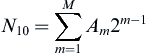 (56)
(56)
For example, the decimal equivalent of the binary number 1010 (i.e., M = 4) is given by
![]()
As mentioned above, another coded number system can be formed from binary by grouping bits to form a new base (as long as it is an integer power of 2). For example, an octal number system is base 8 which uses octal digits such that ![]() In such a system, which can be implemented by groups of three transistor switches to yield eight possible combinations an octal number (denoted N8, with AM being the most significant digit) is given by
In such a system, which can be implemented by groups of three transistor switches to yield eight possible combinations an octal number (denoted N8, with AM being the most significant digit) is given by
![]()
The decimal equivalent of N8 is given for an M-digit octal number by
 (57)
(57)
Logic Circuits (Combinatorial)
Digital computers can perform binary digit (bit) manipulations very easily by using three basic logic circuits, which perform arithmetic or logical operations on binary numbers or logical variables and are often euphemistically called “gates.” We begin with three basic digital gates: the NOT, the AND, and the OR gate. Digital gates operate on logical variables that can have one of two possible values (e.g., true/false, saturation/cutoff, or 1/0). As was previously explained, numerical values are represented by combinations of 0 or 1 in a binary number system.
As mentioned earlier, digital circuits operate with transistors in one of two possible states – saturation or cutoff. Since these two states can be used to represent multiple-digit binary numbers. The input and output voltages for such digital circuits will be either “high” or “low,” corresponding to 1 or 0. High voltage means that the voltage exceeds a high threshold value that is denoted VH. If the voltage at the input or output of a digital circuit is denoted V, then symbolically, the high voltage condition corresponding to logical 1 is written as
![]() (58)
(58)
Similarly, low voltage (corresponding to logical 0) means that voltage V is given by
![]() (59)
(59)
where VL denotes the low threshold value. The actual values for VH and VL depend on the technology for implementing the circuit. Representative values are VH = 2.4 V and VL = 0.8 V for bipolar transistors.
Digital circuit operation is represented in terms of logical variables that are denoted here with uppercase letters. For example, in the next few sections A, B, and C represent logical variables that can have a value of either 0 or 1.
NOT Gate
The NOT gate is a logic inverter. If the input is a logical 1, the output is a logical 0. If the input is a logical 0, the output is a logical 1. It changes zeros to ones and ones to zeros. The simple bipolar transistor circuit of Figure 3.23 performs the same function if operated from cutoff to saturation. A high base voltage (logical 1) produces a low collector voltage (logical 0) and vice versa. Figure 3.24a shows the schematic symbol for a NOT gate. Next to the schematic symbol is what is called a truth table. The truth table lists all of the possible combinations of input A and output B for the circuit. The logic symbol is shown also. The logic symbol is read as “NOT A.” The bar over a logical variable indicates the logical inverse of the variable; that is, if A = 1, then ![]() .
.
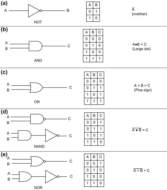
Figure 3.24 Logic “gates.”
AND Gate
The AND circuit effectively performs the logical conjunction operation on binary numbers or logical conditions. The AND gate has at least two inputs and one output. The one shown in Figure 3.24b has two inputs. The output is high (1) only when both (all) inputs are high (1). If either or both inputs (or any) are low (0), the output is low (0). Figure 3.24b shows the truth table, schematic symbol, and logic symbol for this gate. The two inputs are labeled A and B. Notice that for two inputs there are four combinations of A and B, but only one results in a high output. In general, for N inputs, there are 2N combinations with only one having a high (logic 1) output.
OR Gate
The OR gate, like the AND gate, has at least two inputs and one output. The one shown in Figure 3.24c has two inputs. The output is high (1) whenever one or both (any) inputs are high (1). The output is low (0) only when both inputs are low (0). Figure 3.24c shows the schematic symbol, logic symbol, and truth table or the OR gate.
In addition to the AND, OR, and NOT logical circuits, there are combinations of AND and NOT yielding the so-called NAND gate. Similarly, the combination of OR with NOT yields the so-called NOR gate. Combining these two pairs of functions in a single circuit is often advantageous for building up larger digital circuit subsystems or systems on a single IC. Figures 3.24d and 3.24e depict the schematic symbols for the NAND and NOR, respectively, along with truth tables and logical symbols.
Combination Logic Circuits
Still another important logical building block that can be build up with the three basic logic gates is the exclusive OR denoted XOR. This circuit has logical 1 output if one and only one of its inputs is nonzero. A two-input example is shown in Figure 3.25a. The schematic symbol for this device is depicted on the upper left of Figure 3.25a. Its implementation using the three basic gates is shown at the lower left. The XOR truth table and logic symbol are also given in Figure 3.25a.
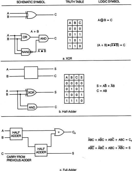
Figure 3.25 Combination logic circuit.
All of these gates can be used to build digital circuits that perform all of the arithmetic functions of a calculator or computer. Table 3.1 shows the addition of two binary bits in all the combinations that can occur. Note that in the case of adding a 1 to a 1, the sum is 0, and a 1, called a carry, is placed in the next place value (in a place position number sequence) so that it is added with any bits in that place value. A digital circuit designed to perform the addition of two binary bits is called a half adder and is shown in Figure 3.25b. Note that it incorporates an XOR gate. It produces the sum and any necessary carry, as shown in the truth table.
Table 3.1 Addition of binary bits.

A half-adder circuit does not have an input to accept a carry from a previous place value. A circuit that does is called a full adder (Figure 3.25c). A series of full-adder circuits can be combined to add binary numbers with as many digits as desired. Any digital computing system from a simple electronic calculator to the largest digital computer performs all arithmetic operations using full-adder circuits (or some equivalents) and a few additional logic circuits. In such circuits, subtraction is performed as a modified form of addition by using some of additional logic circuits as explained in Chapter 4. Multiplication of two 1-bit numbers is characterized by elementary rules of multiplication:

Multiplication of an N-bit number by an M-bit number is implemented under program control in some form of stored program computer as explained in Chapter 4.
Of course, the addition of pairs of 1-bit numbers has no major application in digital computers. On the other hand, the addition of multiple-bit numbers is of crucial importance in digital computers and, of course, in automotive digital control systems. The 1-bit full-adder circuit can be expanded to form a multiple-bit-adder circuit. By way of illustration, a 4-bit adder is shown in Figure 3.26. Here, the 4-bit numbers in place position notation are given by
![]()
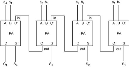
Figure 3.26 4-bit-adder circuit.
where each bit is either 1 or 0. The sum of two 4-bit numbers has a 5-bit result, where the fifth bit is the carry from the sum of the most significant bits. Each block labeled FA is a full adder. The carry out (C) from a given FA is the carry in (C) of the next-highest full adder. The sum S is denoted (in place position binary notation) by
![]()
Logic Circuits with Memory (Sequential)
The logic circuits discussed so far have been simple interconnections of the three basic gates NOT, AND, and OR. The output of each system is determined only by the inputs present at that time. These circuits are called combinatorial logic circuits. There is another type of logic circuit that has a memory of previous inputs or past logic states. This type of logic circuit is called a sequential logic circuit because the sequence of past input values and the logic states at those times determine the present output state. Because sequential logic circuits hold or store information even after inputs are removed, they are the basis of semiconductor computer memories.
R–S Flip-Flop
A very simple memory circuit can be made by interconnecting two NAND gates, as in Figure 3.27a.

Figure 3.27 Sequential logic circuits.
A careful study of the circuit reveals that when S is high (1) and R is low (0), the output Q is set high and remains high regardless of whether S is high or low at any later time. The high state of S is said to be latched into the state of Q. The only way Q can be unlatched to go low is to let R go high and S go low. This resets the latch. This type of memory device is called a reset–set (R–S) flip-flop and is the basic building block of sequential logic circuits. The term “flip-flop” describes the action of the logic level changes at Q. Notice from the truth table that R and S must not be 1 at the same time. Under this condition, the two gates are logically indeterminate and the final state of the flip-flop output is uncertain.
JK Flip-Flop
A flip-flop where the uncertain state of simultaneous inputs on R and S is solved is shown in Figure 3.27b. It is called a J–K flip-flop and can be obtained from an R–S flip-flop by adding additional logic gating, as shown in the logic diagram. When both J and K inputs are 1, the flip-flop changes to a state other than the one it was in. The flip-flop shown in this case is a synchronized one. That means it changes state at a particular time determined by a timing pulse, called the clock, being applied to the circuit at the terminal marked by a triangle. The little circle at the clock terminal means the circuit responds when the clock goes from a high level to a low level. If the circle is not present, the circuit responds when the clock goes from a low level to a high level. As is shown below, there are many uses at J–K-type circuits for their equivalent implementation in computers, which operate with a clock as explained later.
Synchronous Counter
Figure 3.28 shows a four-stage synchronous counter. It is synchronous because all stages are triggered at the same time by the same clock pulse (Clk). It has four stages; therefore, it counts 24 or 16 clock pulses before it returns to a starting state. The timed waveforms appearing at each Q output are also shown. The waveforms of Figure 3.28b indicate how such circuitry can be used for counting, for generating other timing pulses, and for determining timed sequences.
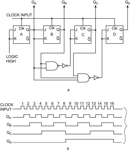
Figure 3.28 Synchronous counter circuit.
Register Circuits
One of the most important circuits for building a computer is formed using multiple JK-type circuits as depicted in Figure 3.29. Such circuits are known as registers. Figure 3.29 is shown as a 4-bit device simply to explain the operation of the register. Practical register circuits used in computers normally have many more JK-type circuits than depicted here. There are many classes of register depending upon usage in the computer and the operation performed. These operations include

Figure 3.29 Storage register circuit example.
When used as a storage register or memory, the data to be shared (which, for example, might be digital input data from a sensor and (A to D) converter), the output of a full adder, or the contents of another register) are provided to the J inputs. The data A4A3A2A1 are transferred to the corresponding Q output at the clock time. It will remain there until new data and a clock pulse are provided to the computer.
Shift Register
Another very important circuit that is implemented with a JK type of circuit (or its functional equivalent) is a so-called shift register. Figure 3.30a depicts a simple 4-bit shift register having the capability of so-called parallel load in which all data bits are transferred simultaneously into the corresponding flip-flop with control C high at the clock pulse.

Figure 3.30 4-bit shift register circuit example.
This latter register has two modes of operation: 1) transfer of data (A4A3A2A1) into the register with control C high and 2) shift right or left with control C low. The shift operation refers to changing the position of a bit in a digital number to a higher (shift left) or lower (shift right) position. Consider an M-bit binary number N,
![]()
where AM is the most significant bit. Shift right or left is a synchronous operation, in that it is associated with clock time tn. A shift left at time tn+1 means that Am becomes Am+1. Similarly a shift right operation means that the Am bit at tn becomes Am−1 at tn+1. For the example circuit of Figure 3.30a, the operation is a shift left. The same circuit could be made into a shift-right operation by reversing the data order; that is, the most significant bit (AM) is entered into JK1, then in a decreasing order until the least significant is loaded into JK4.
The circuit of Figure 3.30 depicts a data load operation that is said to be parallel in which all bits are loaded synchronously. It is also possible to load the data serially in which the data bits are entered in sequence, beginning with either the most or the least significant bit. At each clock cycle, the bits are shifted one position right or left depending upon circuit configuration and/or program control.
The data to be entered into this register consist of a sequence of bits Am that are synchronous with the clock. At each clock pulse, the corresponding data bit (i.e., either a 0 or a 1) is presented along the data line (D in Figure 3.30b). Prior to clock time tn, the previous data bit (i.e., at clock time tn−1) is stored in Q1 and that at time tn−2 in Q2, etc. Each of these bits is presented to the J input of the next flip-flop. The result of the circuit operation is a shift to the next bit position for each clock pulse.
There are additional categories of shift register that perform various logical operations on binary numbers or data depending upon how the circuit treats the least and most significant bits. A shift-right operation drops the A1 bit and shifts a 0 into the AM bit location. The reverse is true for a shift-left operation.
It is also possible to connect the least and most significant bit locations; such an operation is termed “rotate right or left.” For a rotate-right operation, the least significant bit at tn becomes the most significant bit at tn+1. Similarly, the reverse is true for a rotate-left operation. Such operations can be implemented either with dedicated (hard-wired) circuits or more commonly through program-controlled switching.
Digital electronic systems send and receive signals made up of ones and zeros in the form of codes. The digital codes represent the information that is moved through the digital systems by the digital circuits. Digital systems are made up of many identical logic gates and flip-flops interconnected to do the function required of the system. As a result, digital circuits are ideal for implementation in integrated circuits (ICs) because all components can be made at the same time on a small silicon area.
Integrated Circuits
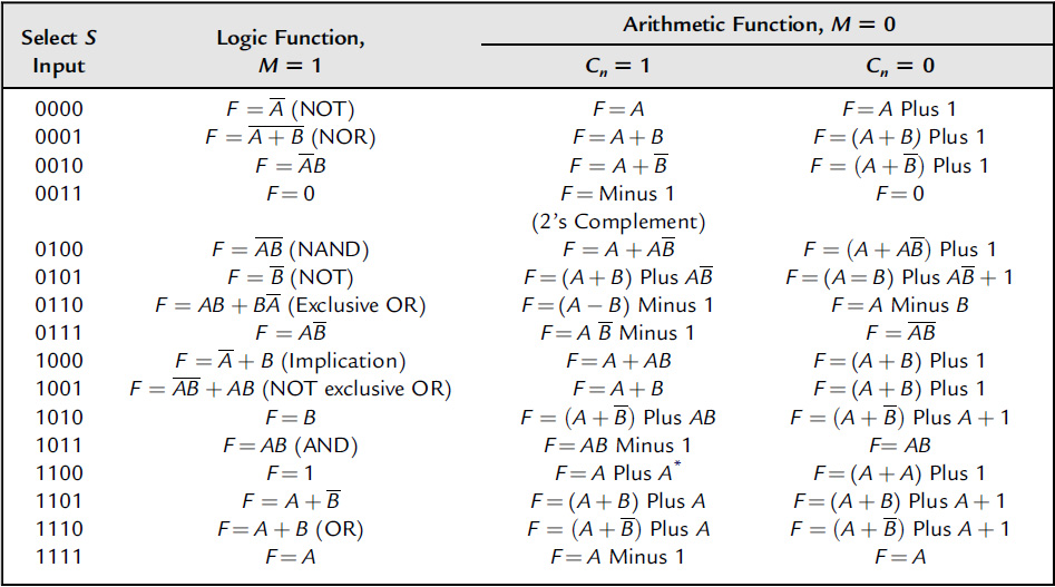
One of the important consequences of integrated circuit (IC) technology progress has been that digital circuits have become available (in IC form) as electronic systems or subsystems; that is, the functional capability of digital circuits in single IC packages, or chips, has spectacularly increased in the past 40 years. One of the important digital systems that is available as an IC is the arithmetic and logic unit (ALU).
Figure 3.31 is a sketch of a typical ALU showing the various connections. This 4-bit ALU has the capability of performing 16 possible logical or arithmetic operations on two 4-bit inputs, A and B. Table 3.2 summarizes these various operations using the logical notation explained earlier in this chapter. The ALU (implemented with more than 4-bits) is an important component of the most important single-chip IC for all digital electronic systems: the microprocessor.
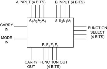
Figure 3.31 ALU symbol.
Table 3.2 Arithmetic logic functions.
The Microprocessor
Perhaps the single most important digital IC to evolve has been the microprocessor (MPU). This important device, incorporating hundreds of thousands of transistors in an area of about ¼-inch square, has truly revolutionized digital electronic system development. A microprocessor is the operational core of a microcomputer and has broad applications in automotive electronic systems.
The MPU incorporates a relatively complicated combination of digital circuits including an ALU, registers, and decoding logic. A representative (though simplified) MPU block diagram is shown in Figure 3.32. The double lines labeled “bus” are actually sets of conductors for carrying digital data throughout the MPU. A block diagram of a microprocessor/microcontroller with more detail is given in Chapter 4. Common IC MPUs use 8, 16, or 32 (or higher multiples of 8) conductor buses.
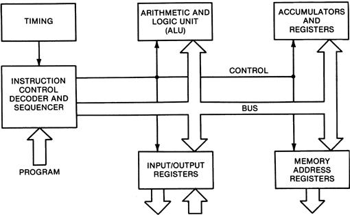
Figure 3.32 Simplified microprocessor block diagram.
Early twenty-first-century automobiles incorporate dozens of microprocessors that are applied for a variety of uses from advanced powertrain control to simple tasks such as automatic seat and side-view mirror positioning. A microprocessor by itself can accomplish nothing. It requires additional external digital circuitry as explained in the next chapter. One of the tasks performed by the external circuitry is to provide instructions in the form of digitally encoded electrical signals. By way of illustration, an 8-bit microprocessor operates with 8-bit instructions. There are 28 (or 256) possible logical combinations of 8 bits, corresponding to 256 possible MPU instructions, each causing a specific operation. A complete summary of these operations and the corresponding instructions (called microinstructions) is beyond the scope of this book. A few of the more important instructions are explained in the next chapter, which further expands the discussion of this important device.