
Carbon Nanotubes
Some of the first discovered and widely studied/publicized nanoscale materials are those of carbon allotropes. Prior to the advent of nanotechnology, three forms of carbon were known: graphite, diamond, and amorphous carbon. Now many other forms of carbon have been discovered that exhibit novel properties, including fullerenes, carbon nanotubes, and graphene (individual graphitic sheets). Chapter 3 provides a summary of materials, including their properties, synthesis, and applications.
Keywords
Carbon nanotubes; graphene; C60; electrical properties; nanomaterials synthesis
3.1 Allotropes of Carbon and Structure
3.1.1 Allotropes of Carbon
As a nonmetallic element, carbon is a group 14 element located in the second period of the periodic table. Its chemical symbol is C, with the atomic number of 6 and the electronic configuration of [He]2s22p2. Carbon is widely distributed in nature, is found in all living organisms, and is in the atmosphere and the Earth’s crust. It is well known that carbon exists in crystalline and amorphous forms in many different allotropes. Examples of amorphous carbon are anthracite, bituminous coal, peat, and lignite. Historically speaking, only two kinds of crystalline forms of carbon were previously known: diamond and graphite. However, things changed in 1985 with the discovery of C60 and C70 and with the discovery of carbon nanotubes (CNTs) in 1991. Recently, Andre Geim, a professor of astrophysics in Manchester, found the existence of a single atomic layer of graphite (graphene), which attracted interest of many research groups and won Andre Geim the Nobel Prize in 2010. Graphene is known to possess very interesting properties that can be applied to many fields, including electronic engineering, nanomechanics, and quantum computing. Diamond, graphite, fullerene (C60), CNTs, and single-layer graphite (graphene) are in the carbon allotrope family.
3.1.2 Structures of Carbon Allotropes
There are differences between diamond, graphite, fullerene (C60), and CNTs in their structure and bonding orbitals. Graphene is a single C atom layer in graphite. Here, we focus on the structural characteristics of diamond, graphite, fullerenes, and CNTs (Figure 3.1).
Graphite consists of sp2 carbon bonding in a planar structure, where carbon is integrated in covalent bonds with the van der Waals force between layers. Because of this structural arrangement, graphite is a good conductor of electricity.
In diamond, carbon has a three-dimensional structure with sp3 covalent bonding, and it is a poor conductor of electricity. Diamond is a nonequilibrium form of C and will transform to graphite over time (although the timescale is approximately 5 million years). If heated or under impact of high-energy particles, then the change can be accelerated.
C60 was discovered in 1985 jointly by H. W. Kroto from the University of Sussex in the United Kingdom and R. E. Smalley and R. F. Carl from Rice University in the Unites States. For this discovery, they won the 1996 Nobel Prize in Chemistry. The structure of C60 has interesting features; the carbon atoms are in sp2 bonding states, with 12 pentagons and 20 hexagons plus 30 π bonds and 90 σ bonds.
In January 1991, Sumio Iijima, a Japanese physicist from NEC Tsukuba Research Laboratory, found that multi-wall carbon nanotubes (MWNTs) can be made using high-resolution electron microscopy in the analysis of carbon fiber produced from arc discharge. An MWNT is a kind of tubular carbon molecule, with each carbon atom being sp2-hybridized on the tube. Between them, the carbon–carbon σ bonds form a hexagonal honeycomb-like structure as the skeleton of the tubes. On each of the carbon atoms, there is a pair of π electrons not involved in the bonding that forms a conjugated π electron cloud across the entire CNT. Depending on the differences of layers, CNTs are categorized into single-wall carbon nanotubes (SWNTs) and MWNTs. Being ultrafine in the radial direction, nanotubes are strictly nanoscale in size. Tens of thousands of nanotubes can be equivalent to the width of a piece of hair. In the axial direction, the nanotubes can be up to tens or hundreds of microns. In 1993, both NEC and IBM discovered SWNTs.
The diameter of a CNT is generally between 0.4 and 50 nm, its length is 1 μm or more, and density is 1.3–1.4 g/cm3 (these features are like that of wool or cotton). Its thermal conductivity is 23.2 W (cm K)−1 (similar to diamond). Its electrical conductivity is dependent on its diameter and ranges from 10−3 to 10−4 Ω cm (similar to the semiconductor germanium) or 5.1×10⁻⁶ Ω cm (similar to copper).
Previous studies claimed that CNTs have limits in diameter. Generally speaking, SWNTs have a diameter from l to 6 nm, with some examples of smaller diameters of only 0.4 nm. Theoretically, 0.4 nm is the smallest possible diameter. If the size is reduced further, then the angle between the carbon atoms will become too small, and that may result in unstable structures. In addition, an SWNT with a large diameter is not a stable structure. Generally, if the diameter is larger than 6 nm, then the tube wall becomes unstable and is prone to collapse.
Regarding the length of the CNTs, the current laboratory preparation methods available can produce a length of SWNTs that is much shorter than that of MWNTs. SWNTs typically have a length of hundreds of nanometers to a few microns, whereas the length of MWNTs is generally in the tens of microns or more (the longest are up to a few mm). MWNTs have a layer of spacing of approximately 0.34 nm, whereas the diameter has a range of 0.4 nm to several thousand nm (depending on the number of layers of CNTs).
3.1.3 Graphene [1]
3.1.3.1 Single-Layer Graphite Material (Graphene) [1]
Graphene is a single layer of carbon atoms densely packed in a honeycomb crystal lattice. This material can be produced by the rapid separation of an atomic layer of graphite. It is a stable, flexible, and robust material with high conductivity. We know that graphite is a composition of carbon. Schematically, the structure of graphene is formed by layers of graphite atoms being vertically torn like paper. Graphene has become a model system in condensed matter physics, because its charged particles can move at relativistic speeds, as if they do not have any mass. This feature has led to some peculiar electronic transport properties. For example, in a graphene layer sandwiched between two superconducting electrodes, a superconducting current can flow at low temperatures, loaded by either electrons or the holes, depending on the gate voltage and also the charge density in the graphene layers.
Interestingly, a limited current can flow through graphene even if the charge density is zero. These observations provide clues to study the relativistic phenomenon, known as time-reversal symmetry, and the electron transport mechanism in graphene.
Regarding electronics in a graphene layer, there will be no scattering in the sub-microdistance. This provides the conditions for the manufacture of speed distribution transistors. At present, a graphene single-electron transistor (SET) has been realized in the laboratory.
3.2 Types and Nature of CNTs
3.2.1 Types of CNTs
As mentioned, CNTs are seamless tubular nanocrystals formed by the curved graphite layer. Graphite consists of sp2 carbon bonding in a planar structure. In CNTs, carbon on the plane is combined with a covalent bond into a honeycomb-like structure, and carbon hexagons curl up into CNTs.
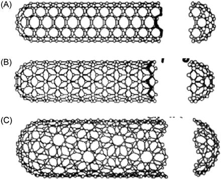
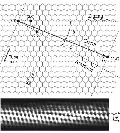
The hexagonal crimping of planar carbon atoms can start from different angles, resulting in different CNTs. There are three different forms, or chiralities, of SWNTs, namely the Armchair, Zig-Zag, and the Chiral types (see Figure 3.2 and 3.3).
3.2.2 Characteristics of CNTs
3.2.2.1 Mechanical Properties
The sides of CNTs are composed of hexagonal carbon rings (graphite sheet); however, at the cap-shaped part where the tube body is bent and the tube is capped, carbon atoms are structured in a number of pentagonal and heptagonal rings. Because the carbon–carbon covalent bond that constitutes these different carbon ring structures is one of the most stable chemical bonds in nature, CNTs are expected to present very good mechanical properties, with strength close to that of the carbon–carbon bond. Studies have shown that the strength of CNTs is 100 times that steel, but with only one-sixth the density.
CNTs have outstanding flexible features (extension rate of up to 30%); they can be bent into a small angle or into a tiny ring structure. When the bending stress is removed, the CNTs can be completely restored to their original state from the large bending deformation. Under great external stress, a brittle fracture will not occur. Fibrous materials consisting of nanotubes with good mechanical properties will have many applications in the future in the industrial sector. One such example is for use as cables in a space elevator, a theoretical device that can transport goods and people from the Earth to space stations. CNT cables might be the only material that will not be broken because of its weight.
3.2.2.2 Electrical Characteristics
Different types of CNTs vary in their conductive properties: for single-wall nanotubes with metallic conductivity, the one-third saw tooth-shaped CNT comes with metal features, whereas the two-thirds palm-shaped CNT has a semiconductor character. The CNTs of semiconductor nature will have a narrower band gap as diameter increases. In the case of large diameters, the band gap is zero and shows metallic features.
Because the electronic flow of CNTs is restrained by the quantum confinement, electrons in CNTs usually have axial movement only along CNTs in the same direction as the layer of the graphite sheet, whereas radial movement will be greatly limited.
These electrical properties of CNTs can enable widespread applications in the future in nanoelectronics. For example, metallic CNTs can be used as connection lines in nanometer-integrated circuits (ICs), whereas the semiconductor nature of CNTs can be used to produce nanoelectronic switches and other nanometer quantum devices.
Tests of the field emission effect of MWNTs found that the measured resistance values of CNTs follow Ohm’s law.
R. E. Smalley, the 1996 Nobel Prize winner, performed his study in 1995 by imposing −100- to −110-V bias voltages to open nanotubes, which produced 0.5- to 1.5-mA field emission currents. With the help of a CCD camera, the tips of nanotubes could be observed to emit very weak incandescent light. In the same year, De Heer, André Chatelain, and Daniel Urgate also first proposed the idea of using CNTs as field emission devices.
3.2.2.3 Thermal Properties
Studies revealed that CNTs have superior thermal conductivity.
David Tomanek at Michigan State University found in his experiments that the measurement of thermal conductivity of CNTs could be as high as 3,000 W/m/K, almost identical to the thermal conductivity of diamond, and he predicted that in the future it could reach 6,600 W/m/K. Thermal conductivity of this magnitude can be applied in future circuits by transporting heat away from dense circuits, a current issue in IC construction and design.
Similarly, researchers at the University of Pennsylvania found that CNTs are currently the world’s best thermal conductivity material because of their transmission speed of up to 10,000 m/s by way of ultrasonic heat transfer. The study also revealed that even if they were bound together, the heat would not be transferred from one CNT to another. This shows that CNTs can only be one-dimensional in the direction of heat transfer.
In addition, research has shown that CNTs are ballistic wires with ballistic conductance. At room temperature, the electrons can pass through wires without any resistance and backward scattering to produce heat. In the tests performed at Georgia Institute of Technology, for example, the researchers applied 10 million amps/cm of current through the CNTs. They found that the resistance of MWNTs is a constant that is independent of their lengths and widths.
3.2.2.4 Superconducting Phenomenon of CNTs
Mathieu Kociak, who worked for CNRS laboratories in Paris-South University, claimed that the phenomenon of superconductivity was observed in nanotube ropes. This means that the phenomenon of superconductivity was first discovered in a system with minimal conduction channels, because super-current is required to pass CNTs of the substrate material in the two-dimensional network structure with lack of contents. The researchers expected to increase the transition temperature by means of proper ion implantation. The current transition temperature is only 300–400 mK.
3.2.2.5 Chemical Properties
The use of CNTs can improve the performance of an atomic force microscope. For example, Harvard’s John Hafner placed a 0.9- to 2.8-nm diameter CNT at the tip of an atomic force microscope probe. Nanotubes used as microprobes will increase not only the resolution but also the applicability in the study of the nature of adhesion between the sample and the scanning tip. Hafner called such methodologies chemical force microscopy.
In addition, Masako Yudasaka at NEC Laboratories, Japan, placed C60 molecules into CNTs, resulting in very high pressure values. C60 can only generate a force of micro-newtons; however, divided by the area of CNTs, it will cause a pressure of 0.1 GPa. This discovery will lead to novel changes in fullerenes for chemical applications. Yudasaka also claimed that CNTs with a cone-shaped tip, which have a diameter of 2 nm, length of 50 nm, and an open angle of 20°, will be able to supersede activated carbon in filters used to absorb gases.
3.2.3 Electronic Structure of CNTs
3.2.3.1 π-Electron Orbital and the Energy of the Conjugated Molecule in Planar Structure
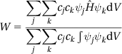
In 1931, the German physicist E. Hückel proposed the Hückel equation based on the Schrödinger equation. The solutions to eigenvalues and eigenvectors of the Hückel equation obtained the π electron orbital and the energy of conjugated molecules in planar structures. This showed that because of the way the carbon electron cloud of benzene is distributed in the ground state, it is surrounded on both sides, and this also explained some of the current-related phenomena. The Hückel equation is a useful tool for calculating the electron structure of graphite, graphene, C60, and CNTs. The following is a brief description of this theory [2].
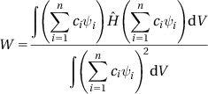
An electron in a molecule occupies a molecular orbital (MO). Assuming the wave function for an MO is expressed by Ψ![]() , then Ψ
, then Ψ![]() can be expressed by a linear combination of atomic orbitals:
can be expressed by a linear combination of atomic orbitals:
Ψ=∑ni=1ciψi (3.1)
Here, ψi![]() is the atomic orbital wave function. The energy W of the MO can be obtained by multiplying by the left side of the Schrödinger equation:
is the atomic orbital wave function. The energy W of the MO can be obtained by multiplying by the left side of the Schrödinger equation:
ΨˆHΨ=ΨWΨ (3.2)
Using a volume integral
W=∫ΨˆHΨdV∫Ψ2dV (3.3)
we substitute Eq. (3.3) with Eq. (3.1) to get
W=∫(n∑i=1ciψi)ˆH(n∑i=1ciψi)dV∫(n∑i=1ciψi)2dV (3.4)
 (3.4)
(3.4)
Recombining the sum we get
W=∑j∑kcjckψjˆHψkdV∑j∑kcjck∫ψjψkdV (3.5)
 (3.5)
(3.5)
Using the equations
Hjk=∫ψjˆHψkdV (3.6)
Sjk=∫ψjψkdV (3.7)
Eq. (3.5) can be rewritten as
W∑j∑kcjckSjk=∑j∑kcjckHjk (3.8)
Recombination of the sum terms gives
W∑jckSik+W∑kcjSji=∑kckHik+∑jcjHji (3.9)
For Hjk=Hkj,Sjk=Skj![]() Eq. (3.9) can be rewritten as
Eq. (3.9) can be rewritten as
W∑kckSkj=∑kckHjk (3.10)
or
∑kck(Hkj−WSkj)=0 (3.11)
According to Eq. (3.11) and the conditions of a nonmediocre solution, the secular equation is obtained as
|H11−WS11H12−WS12⋯H1n−WS1nH21−WS21H22−WS22⋯H2n−WS2n⋮⋮⋮⋮Hn1−WSn1Hn2−WSn2⋯Hnn−WSnn|=0 (3.12)
 (3.12)
The energy of the molecules is available from the solution of this secular equation.
Hückel introduced an approximate method that can be used to simplify the solution of the secular equation. It is called the Hückel MO method (the HMO method) and has three assumptions, as follows:
Using these assumptions, for ethylene, secular Eq. (3.12) can be reduced as:
|α−Wββα−W|=0 (3.13)
As x=(α−W)/β![]() , then Eq. (3.13) is changed to
, then Eq. (3.13) is changed to
|x11x|=0 (3.14)
That is,
x2−1=0 (3.15)
So, x=±1![]() . Thus,
. Thus,
W=α±β (3.16)
Here, W=α+β![]() corresponds to the bonding state π
corresponds to the bonding state π![]() -MO and W=α−β
-MO and W=α−β![]() corresponds to the anti-bonding state π*
corresponds to the anti-bonding state π*![]() -MO.
-MO.
To calculate the coefficient of the wave function, we substitute the energy value into the secular equation:
c1(α−W)+c2β=0c1β+c2(α−W)=0 (3.17)
As W=α+β![]() , c1=c2
, c1=c2![]() is given, and as W=α−β
is given, and as W=α−β![]() , c1=−c2
, c1=−c2![]() is given, by the use of normalization condition
is given, by the use of normalization condition
∫Ψ2dV=1 (3.18)
and as Eq. (3.1) is similar to the Hückel equation, Eq. (3.18) can also be expressed as:
∑j∑kcjckSjk=∑c2i=1 (3.19)
|c1|=|c2|=1/√2![]() is given.
is given.
3.2.3.2 Electronic Structure of Graphite
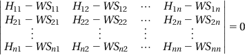
Using the aforementioned method, we can calculate the energy dispersion relation for graphite electronics [3]:
W2D(kx,ky)=±γ0[1+4cos(√3kxa2)cos(kya2)+4cos2(kya2)]1/2 (3.20)
This relationship is essential for the calculation of the electronic structure of CNTs.
Energy dispersion relations for graphite are applicable in the calculation of the electronic structure of CNT electronics. Figure 3.4 is the electronic structure of armchair-shaped CNTs with periodic boundary conditions. Armchair-shaped CNTs are ideal materials for production of one-dimensional quantum wires.
3.3 Preparation of CNTs
The common methods used for the preparation of CNTs mainly include arc discharge, laser ablation, chemical vapor deposition, solid-phase pyrolysis, glow discharge, gas combustion, and polymerization synthesis.
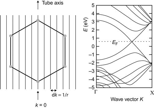
The arc discharge method is the oldest major method for the production of CNTs (Figure 3.5). In 1991, Japanese physicist Sumio Iijima used this method to produce carbon fiber and discovered CNTs for the first time. The arc discharge method works as follows: a graphite electrode is placed in a reaction vessel filled with helium or argon gas to stimulate the arc between the two poles. At this point, the temperature can reach 4,000°C.
Graphite will evaporate under this condition to generate products, including fullerenes (C60), amorphous carbon, and SWNTs or MWNTs. By controlling the catalyst and hydrogen content in the container, the relative yields of several products can be adjusted. Technically, it is relatively simple to use this method to prepare CNTs. However, the CNTs produced in this way may be mixed with C60 and other products, and it may be difficult to obtain the products with high allotrope purity. Furthermore, the products are often MWNTs rather than SWNTs, limiting the scope of this method for practical research. In addition, the method tends to consume excessive energy in the reactions. In recent years, some researchers have found that if molten lithium chloride is used as the anode, it can effectively reduce the energy consumed in such reactions and make it easier to obtain higher purification.
In recent years, a chemical vapor deposition method has been developed to overcome the shortcomings using the arc discharge method. This approach enables gaseous hydrocarbons to pass through a template with catalyst particles attached. Gaseous hydrocarbons can then be decomposed to form CNTs at temperatures of 800–1,200°C. The highlighted advantage of this method is that the residual reactants of gas can leave the reaction system to obtain CNTs with high purity. At the same time, there is no need to have a very high temperature, so the energy required in this process is comparatively lower than that for arc discharge experiments. However, the CNTs made with this process have irregular diameters and shapes, and a catalyst must be used in the preparation process. Research is currently being performed to control the structure of CNTs generated by chemical vapor deposition, including controlling the arrangement of the catalyst template.
Other methods include solid-phase pyrolysis. It is a new method by which a conventional carbon-containing sub-solid body undergoes pyrolysis at high temperatures for the growth of CNTs. This approach allows a relatively stable process and does not require a catalyst. However, it is limited by the availability of raw materials, so scaled and continuous production cannot be achieved.
In addition, there are ions or laser sputtering methods. Although it is easy to achieve continuous production with these two methods, the scale is limited because of equipment limitations.
3.4 Applications of CNTs
3.4.1 CNT Electronics
3.4.1.1 The Limits of Microelectronics Technology and the Emergence of Nanoelectronics
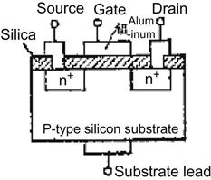
The transistor is the most vital component in electronic circuits. Of all types of transistors, metal oxide semiconductor field-effect transistor (MOSFET) is particularly important because of ease of integration into ICs. As shown in Figure 3.6, MOSFET has three electrodes, namely source, drain, and gate; gate is responsible for controlling devices by manipulating the volume of current that flows from source to drain.
Many of these transistors, together with a number of other electronic devices such as resistors, capacitors, diodes, and wiring, are integrated in a single chip to constitute an IC. Further combination of ICs with different functions will become the basis of electronic devices in complex equipment such as computers, televisions, and communication equipment. This is analogous to organs in the body, which comprise numerous cells that constitute an organism.
At present, the size of the transistor continues to shrink, whereas the density of electronic devices on unit chips keeps increasing. This is demanded by ultra-miniaturization of devices as well as increases in computing capacity. Intel’s co-founder Gordon Moore described the future development trend of computer chips in 1965. Moore’s view is: “The number of transistors that can be placed inexpensively on an integrated circuit has increased exponentially, doubling approximately every two years.” This is the famous Moore’s law.
Facts have proved that Moore’s law accurately forecasts the development trend of chip technology in the past 30 years. With the increasing integration of ICs, the size of transistors and the line width of ICs are getting smaller and smaller, resulting in a great challenge for Moore’s law. Until 2010, the smallest size of microelectronic devices and the minimum width of IC both have been smaller than 100 nm. This approaches the physical limits of the lithographic processing technology in modern microelectronics, potentially halting the progress of Moore’s law in future semiconductor technology.
Using advanced photolithographic techniques, transistors of narrow size and line width can be etched on silicon, successfully reducing the size of the transistor channel to 0.1 μm (100 nm). However, the further reduction of size scales will be difficult because of limitations in photolithography optics and chemistry. In the lithography process, the minimum line width of processing depends on the selected wavelength of light. At present, light used in current lithographic processes is in the deep ultraviolet region, so it is also known as deep ultraviolet (UV) lithography. Deep UV has a wavelength of 240 nm, and its theoretical limit in lithography is 100 nm. Therefore, current lithographic technology will be unable to process a minimum line width of less than 100 nm. To improve the accuracy of lithography, researchers have been constantly exploring and developing more stable light sources with shorter wavelengths. Many chip manufacturing companies in the United States and Japan and some research institutes in China are developing extreme UV lithography that applies the ultra-UV laser source. With shorter ultra-UV wavelengths, a minimum line width in lithography of 70 nm or less is possible. With the increased precision of lithography, surface uniformity between substrate and the photolithography mask are required to improve with the decrease in feature size. Another bottleneck may be required to improve the size scales and accuracy of lithography.
The beam spot diameter for electron-beam lithography can be made very small, with its etched precision achieving a minimum line width of 10 nm. However, such processes are too slow and expensive for large-scale production. Scanning tunneling microscopy (STM) and atomic force microscopy (AFM) nanoprocessing technologies, unconstructed by the limitations of photolithography and e-beam lithography, are likely to be the preferred tool in the future in the processing of ultra-large-scale ICs.
At present, the key materials for making ICs have also been updated to further improve performance. For example, IBM has replaced aluminum with copper to connect transistors in the circuit. Copper has better conductivity than aluminum, which increases the transmission rate between devices and also makes chips smaller and less expensive.
Current microelectronics technology, in addition to the aforementioned restrictions in lithographic processing technology, is also subject to restrictions of quantum effects in devices and limitations from power dissipation of electronic devices.
At present, electronic devices are actually “current” devices that involve a large number of electronic phenomena that obey the classical theory of electron motion. In the next section, the microprocessor chip is used as an example for discussing the limitations of electronic behavior in microelectronics technology. The chip microprocessor works with the on/off state of logic gates, which is dependent on the availability of current flow. Smaller chip widths will lead to a substantial reduction in the number of electrons that flow through the logic gates in a certain amount of time. When the number of electrons is sustainably reduced, the logic gate will be in a state of uncertainty in determining the “on” or “off” and will not work properly. In addition, a device being reduced to nanoscale may lead to other quantum effects, resulting in some nonclassical behavior of electrons.
Another major limitation in the development of microelectronics technology is the large power consumption that will be demonstrated for such devices. Chip redesign and manufacturing, as well as improvements in the lithographic process, can improve the integration of ICs to a certain extent, but the large operating current power of current microelectronic devices comes with relatively high power consumption. With the substantial increase in chip integration and speed of communication, the speed of electronic flow in the circuit will also increase, which will eventually lead to an exponential increase in the power needed to run the chip properly, potentially resulting in chip failure.
To overcome the limits of microelectronic technology, molecular electronics and nanoelectronics are now of immense research importance. Nanoelectronics mainly involves the electronic, atomic, and molecular motion in the nanoscale patterns, focusing on nanoscale films and wires and various other assemblies, based on quantum properties with respect to the electronic properties, characteristics, and processing/assembly conditions. The performance involves some of the basic issues including amplification, oscillation, pulse technology, and computing processing. The new theory is mainly based on the quantum details of electronics, electronic quantum tunneling effect, noncontinuity of the electronic energy levels, quantum size effect, and statistical fluctuation characteristics.
Quantum effects in nanoelectronic devices exhibit operating currents of 1–10 electrons, and thus have very small energy consumption. Compared with the current microelectronic devices in ultra-large-scale ICs, their power consumption will be greatly reduced. Another significant advantage of nanoelectronic devices is that their working frequency can be increased significantly.
By virtue of today’s microprocessing technology, solid-state electronics channels of very small size can be made to manipulate electron motion through voltage control. Conductance will show a step-like variation as G0. This change is due to the single-electron access to the channel and is called the single-electron effect. The most promising application of the single-electron effect is its use in the electronic features of special conductance material, such as CNTs, C60, and quantum dots (QDs). These materials can be used to create single-electron devices in molecular electronics to be used as SETs, single-electron switches, single-electron circuits, and single-electron logic devices. Therefore, a new discipline, molecular electronics, has emerged. The advent of the SET brings the hope of further reducing the size of electronic devices.
3.4.1.2 Single-Electron Transistor [4–6]
SETs are quite different from the traditional transistor regarding their principles of operation. SETs are novel nanoelectronic devices based on the basic physical principles of the Coulomb blockade effect and the single-electron tunnel effect.
As early as the 1950s, people discovered the Coulomb blockade effect and the single-electron tunneling effect. These effects were not taken advantage of until the 1980s, when they were successfully used to make electronic circuits. The main reason for the delay in practice is simply limitations in manufacturing.
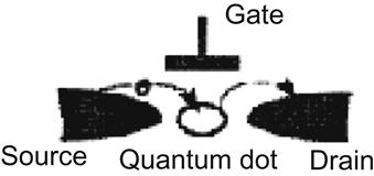
Figure 3.7 is a diagram of an SET, wherein the biggest difference from the traditional transistor is that it allows only one electron from source to drain. This requires electronic access to the channel and the ability to turn off the source by adjusting applied voltage. This enables the election to temporarily stay on an island-like QD, followed by electron transport on an applied voltage to the drain. This is similar to the Panama Canal, where the water level is regulated through the gate opening and closing to allow a ship coming through the canal.
In actual devices, a thin layer of the tunnel junction is in between the QD island and the source and drain. Conductive devices are separated by an insulating material. As the thickness of the insulation between the devices decreases, the electrons will transmit the charge through the insulating layer, resulting in device failure. This is called the quantum tunneling effect in quantum mechanics. If two nanoparticles are connected by a tunnel junction (a very small gap or a very thin insulating layer), then a single electron will pass through the tunnel barrier (tunnel junction) from one nanometal particle to another. This process is called quantum tunneling. To make a single electron tunnel from one nanoparticle to another, the electron is required to have enough energy to overcome the Coulomb blockade of electrons. This process is the single-electron tunneling effect.
The island in the middle is known as the Coulomb island, which is usually a QD 10–100 nm in size. Because the size of the material is close to that of the electron wavelength, the electron confined in QDs comes with discrete energy levels. This is why the QD is called an “artificial atom.” However, according to Heisenberg’s uncertainty principle, the energy has no accuracy. Only when the accuracy of this energy, ![]() E, is far less than the energy gap, Eg, of the QD can the electrons be bound at a certain level. This condition is expressed as:
E, is far less than the energy gap, Eg, of the QD can the electrons be bound at a certain level. This condition is expressed as:
ΔE≪Eg=e2/C (3.21)
where e is the amount of the basic charge and C is the capacitance of QDs. ![]() E can be estimated according to the uncertainty principle:
E can be estimated according to the uncertainty principle:
ΔEΔt≥h (3.22)
Here, h is Planck’s constant. The uncertainty of time, ![]() t, can be approximated as the characteristic time of the equivalent RC circuit formed by the junction and QD:
t, can be approximated as the characteristic time of the equivalent RC circuit formed by the junction and QD:
Δt=RC (3.23)
Here, R is the resistance of the junction. Substituting Eqs. (3.22) and (3.23) into (3.21), we get
R≫h/e2≈26kΩ (3.24)
This means that the junction resistance must be greater than 26 kΩ to ensure the stability of the electron on the same level.
From the energy point of view, the QD and the tunneling junction with high energy on both sides can form a potential well, as shown in Figure 3.8A. Importantly, this energy barrier has limited height on both sides of the QD. Moreover, the voltage can be adjusted to individually increase or decrease the height value, as shown in Figure 3.8B. The source is applied with a negative bias so that the potential energy of the source can be increased to exceed the lowest unoccupied energy level of the QD. The electrons then have the opportunity to penetrate the barrier and flow from the source to the drain, as shown in Figure 3.8C.
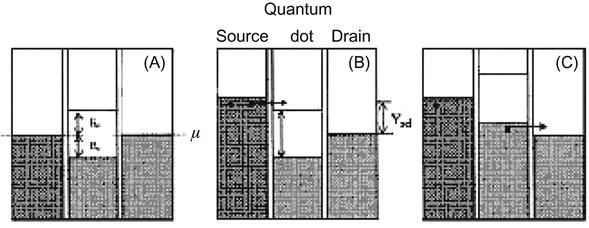
In Figure 3.8, two tunneling junctions and the QD can form a quantum well of energy. By adjusting the applied voltage, the “depth” of the well will change accordingly so as to control the single-electron flow.
An SET is a transistor that has a separate source, drain, and gate. Like the classical FET, current flows between the source and the drain via gate-adjusted electric field control. A major difference in the SET is that only one electron at a time can come through inside the SET. This is strikingly different from the FET, which allows tens of thousands of electrons to flow through at the same time. This difference is caused by the Coulomb blockade effect.
The Coulomb blockade effect is one of the most important physical phenomena observed in the field of solid-state physics in the 1980s. When the size in the physical system reaches a nanoscale order of magnitude, the system will have a noncontinuous charge and discharge process; in other words, it is quantized. To charge an electron, energy, Ec, is required to be e²/2C (charging energy), where e is the electron charge and C is capacitance of the physical system. The smaller the system is, the smaller the capacitor C is, while the energy, Ec, will become greater. This energy can be referred to as Coulomb blockade. In the charging and discharging process in a nanoscale system, the electron cannot undergo continuous mass transfer, but rather single-electron transfer. Such single-electron transfer in a nanomaterial is known as the Coulomb blockade effect.
After an electron enters into a QD from a source, energy levels of the QD will increase accordingly (as compared in Figure 3.8B and C). The increased amount will be charging energy Ec:
Ec=e2/2C (3.25)
The entry of the first electron results in a level increase, which is equivalent to erecting a barrier to the second electron. If the charging energy is greater than the electron energy obtained by a thermal perturbation:
Ec>kBT (3.26)
where kB is the Boltzman constant, then the second electron will not be able to obtain sufficient energy to cross the barrier into the QD until the first electron leaves and the energy levels decrease back to the original level. This is the principle of the Coulomb blockade effect.
The smaller the QD size, the smaller the capacitance and the greater the charging energy will become. For example, when a QD has a diameter of 100 nm, capacitance value of approximately 10–16 F, and relative charging energy of approximately 10−3 eV, the operating temperature is required to be below 4 K to satisfy Eq. (3.26) and to ensure the Coulomb blockade effect. Such a low temperature is clearly not conducive to practical applications. To raise the operating temperature, the size of QDs must be reduced to improve the charging energy. According to estimation, if you want to achieve the Coulomb blockade effect at room temperature (300 K), the QD is expected to have a capacitance value as small as 10−18 to 10−19 F. Accordingly, its size must be less than 10 nm. Based on the current level of technology, it is still rather difficult to prepare such an SET operation at room temperature. This is also a current challenge faced by those in this research field.
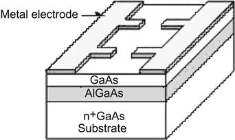
At present, SETs can be divided into four categories by their raw material: (1) semiconductor (silicon, GaAs) SETs; (2) metal SETs; (3) superconductor SETs; and (4) the SET from a CNT, in which the SET is made from semiconductor materials, is easy to integrate and can be used for very-large-scale ICs. Figure 3.9 shows the SET made from semiconductor materials. Compound semiconductors AlGaAs/GaAs with energy gaps of different widths are first stacked to form a quantum well. This is followed by electrode patterning made by lithography.
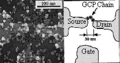
Unlike the aforementioned top-down production process, Figure 3.10 shows gold particles (~10 nm) deposited on the substrate of silicon dioxide, wherein a long chain of three gold particles links the metal source and drain at a distance of 30 nm and works as a Coulomb island required by an SET. This approach is not as good as that of semiconductor technology in terms of precise positioning of the QD. Nonetheless, this technique uses very small nanoparticles to demonstrate the production of room-temperature SETs.
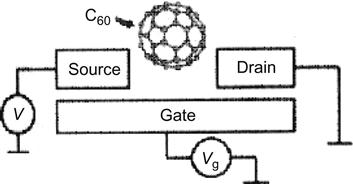
For SETs, the center island can also comprise a single molecule. For example, the center island in Figure 3.11 comprises C60.
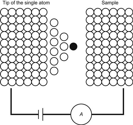
The smallest possible structure of the center island is simply one atom at the center of an SET. Such a configuration would have a minimal tunnel junction capacitance. Practically, it is difficult to place a single-electron atom between the two electrodes that is not connected with the outside world. When a single atom of the STM tip is very close to a sample, this system can be deemed as the basic structure of an SET on the single-atom scale (Figure 3.12).
Compared with conventional transistors, SETs have the advantages of small size, fast transmission, high sensitivity, and, most importantly, low power consumption. The microelectronics at the present time have formally entered the domain of the nanoscale from the sub-micron scale, and the technical limits set by basic physical laws are already in sight. For instance, Moore’s law is beginning to face serious challenges. The SET is likely to be a new generation of electronic devices in the mainstream of the twenty-first century.
3.4.1.3 CNT Electronics [7–9]
Diodes, FETs, and other elements of electronic devices form the basis of silicon-based microelectronics. Similarly, the development of nanoelectronics requires a new materials framework to be built, whereas the field of CNT-based electronics has been considered to be very promising.
The development of CNT electronics will mainly come through the following stages. First, the electrical properties of CNTs must be fully elucidated. Second, the base elements of CNT-based electronic devices need to be identified and developed (that is, those elements corresponding to silicon-based microelectronics, such as diodes and FETs). Third, these electronic devices based on CNTs are used to build a logic circuit with certain functions. Finally, the key issue to be resolved is how to achieve the integration of these circuits reliably on a mass-production scale. At present, CNT electronics research has made great progress in the first two stages. Meanwhile, the third stage of the research work is underway. There are reports that prototype CNT-based logic circuits have been built in laboratories.
3.4.1.3.1 Quantum Wire
The study of quantum wires mainly concentrates on a variety of CNTs. CNTs are the ideal material for quantum wires. Quantum wire made from CNTs is called nanotube quantum wire. Currently, the conductivity of such large molecules is being extensively studied.
Different CNTs can be candidates in the formation of a variety of nonlinear electronic devices. The chirality of CNTs can be used to determine whether these CNTs have the features of being a conductor or a semiconductor. Furthermore, different local defects, such as the existence of five-membered rings and/or six-membered rings, may affect their electronic properties. CNTs can be divided into SWNTs and MWNTs according to their structure. SWNTs are formed by a curling layer of graphite, whereas MWNTs consist of multiple rolled layers (concentric tubes) of graphite.
Conductivity of an SWNT
At low temperatures, SWNTs have a resistance of approximately 1 MΩ between the two ends. Under different voltages, the typical current–voltage curves show a clear diode rectification effect: a one-way pass and the curve showing high nonlinearity at a higher bias.
As a voltage is applied between different electrodes, the same CNT can be found with different electronic behaviors at different locations.
Conductivity of a Single MWNT
SWNTs have a conductance value of 2G0, which is not dependent on diameter or length. MWNT conductance should increase with the number of layers. However, experiments found that the conductance value of MWNTs is only 1G0, because only one layer of CNT contributes to the conductance measurement.
If MWNTs are conductors, then their first layer must be conductive. If the second layer is insulating, then the axial resistance is very large. If this is the case, then this and the following layers will not make any contribution to the conductivity.
It should be noted that CNTs are not the only option for preparing molecular wire; there are other methods available. For example, the method of electrochemical growth can be used to connect two metal nanoparticles with metallic copper wire.
3.4.1.3.2 CNT-Based Junction
CNTs can form a molecular junction, cross-junction, and/or p–n junction. A molecule junction is formed by introducing a pair of pentagon–heptagon (abbreviated as 5–7 pair) defects into an SWNT, and then two or more SWNT segments are connected to form the junction. Cross-junction refers to the junction formed by crossing two SWNTs. The p–n junction is an outcome of the specific modulation-doped action of SWNTs. They all show characteristics shared by the diodes in silicon-based microelectronics.
Studies found that the hexagonal network of SWNTs can be introduced with a 5–7 pair defect to acquire a seamless connection of two or more segments of CNTs with different atomic and electrical structures. Thus, a molecular junction of CNT is formed.
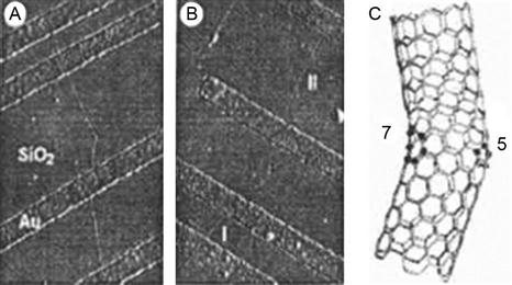
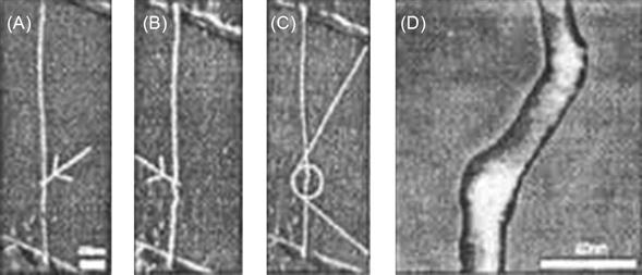
CNTs include two types: metal (abbreviated as M) and semiconductor (abbreviated as S). By introducing a 5–7 pair of defects, two sections of SWNTs are linked to form molecular junctions that may be classified into three categories: MM, MS, and SS. Reports of the electrical properties of MS and MM appeared as early as 1999. It is reported that the MS molecular junction has nonlinear current–voltage (I–V) characteristics like a rectifier diode, whereas the MM molecular junction exhibited conductance dependent on temperature. Figure 3.13A and B show the AFM image of 5–7 pair defects in the molecular junction with CNTs. The angle between the two CNTs is approximately 40°. Figure 3.13C shows the diagram of a molecular junction with a heptagonal recess and a pentagonal convex. As shown in Figure 3.13A, there are three electrodes that are mounted on a molecular junction and two straight CNTs. The CNT molecular junction has an important potential application in producing electronic switches.
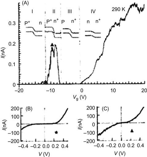
The practice of doping to adjust the energy band plays a very important role in microelectronics. The semiconductor process is actually a “process of control doping.” In today’s microelectronics, the most basic components, such as diodes, bipolar transistors, and FETs, are all achieved through the intrinsic semiconductors being doped. Based on these traditional devices, doped CNTs show the same features and functionality. In 2000, the Dai group reported on the preparation and properties of the p–n junction based on the modulation-doped CNTs. In their experiment, a semiconductor-based SWNT received the axial modulation doping, so that half of it is kept as the p-type while the other half is doped with potassium to form the n-type, forming a p–n junction. I–Vg characteristics are shown in Figure 3.14. This I–Vg characteristic curve is divided into four zones. If the gate voltage Vg is between −20 and −12 V, then the conductance is close to zero (state I); if it is between −12 and −7 V, then the conductance clearly has a peak (state II); if it is between −7 and −1 V, then it decreases to zero again (state III); and if Vg increases to between −1 and 20 V, then the conductance begins to increase almost monotonically as the gate voltage increases (state IV).
3.4.1.3.3 SET with CNTs
The nature of CNTs is closely related to their structures. In terms of electrical conductivity, CNTs can be either a metal or a semiconductor in nature. Even in different parts of a single CNT, changes in the structure can also bring about different conductivities. In addition, the radial motion of electrons in CNTs is limited, showing a typical quantum confinement effect, whereas the axial movement of electrons is not impeded. Therefore, we can say that CNTs are one-dimensional quantum wires. As a typical one-dimensional quantum transport material, metallic CNTs show typical Coulomb blockade effect at low temperatures. As the outer electron enters such a tiny capacitor as the CNT (voltage change: ΔV=Q/C, where Q is the injected charge and C is capacitance of CNTs), capacitors that are small enough to be injected with an electron will produce sufficiently high reverse voltage for the circuit block. After the injected electron comes through the CNT, reverse-blocking voltage will disappear to continue to receive the injected electrons.
As mentioned, the future prospects of traditional silicon-based microelectronics could be encouraging with SETs. However, the majority of SETs need to work at very low temperatures, which severely limits their possible use in practice. Recently, scientists have found that metallic CNTs have strong bending ability, which is manifested as a nanometer-sized tunneling barrier for electron transport. Then, according to the structure of the SET, it can be conceived that the two strong bends of metallic CNTs are combined to form an SET.
In 2001, Postma and associates reported such SETs, which were based on a single-CNT metallic molecule and worked at room temperature. As shown in Figure 3.15A, a metallic-type CNT grows on an Au electrode located on the Si/SiO2 substrate. Then, the AFM probe is used to drag a part of the CNT in the direction of the arrow to produce strong bending. As shown in Figure 3.15B, in the direction of the arrow, the AFM probe drags another part of the CNT to produce strong bending a second time. Figure 3.15C and D present the image of this SET. The “Coulomb island” between the two bending parts forms a segment of CNT of approximately 25 nm.
3.4.1.3.4 CNT-Based FET
In early 1998, Cees Dekker’s group reported an FET that comprised an SWNT that operated at room temperature. The FET included a semiconductor SWNT, to which three metal electrodes were connected. By adjusting the voltage applied to the gate, the CNT could be converted between on-state and insulating state. There had been reports of similar characteristics of metallic SWNTs that worked at extremely low temperatures. Successful construction of the CNT-based FET makes it possible to take a major step forward in CNT-based electronics.
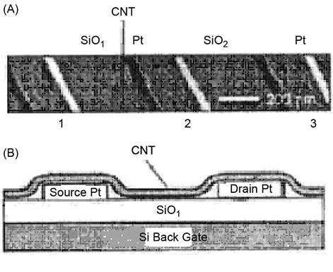
Figure 3.16A shows the AFM image of the connection of an SWNT and three Pt electrodes. On the Si substrate of the semiconductor, the thermal method is used to allow the growth of a layer of SiO2 with a thickness of 300 nm while the Si substrate is used as a back gate, as shown in Figure 3.16B.
The CNT-based FET described is made from semiconductor-type CNTs, whereas the CNT-based SET is made by using metallic CNTs. A key issue is how to effectively separate these two types.
3.4.1.3.5 Complementary Nongate (Inverter) Circuit with CNTs
In August 2001, Avouris and team (from IBM) reported the successful development of two complementary CNT-based nongate circuits, with one being based on a structure of two CNTs and the other being based on a single CNT.
As mentioned, an ordinary FET composed of intrinsic CNTs is p type, but the potassium-doped CNTs can have n-type characteristics. The latest research by Avouris and team also found that the p-type CNT FET can be placed in a vacuum for annealing to become n type, and the oxygen environment can make CNTs turn into p type. Therefore, by applying these properties, the same substrate can be placed with p-type and n-type CNT FETs through appropriate procedures for the composition of a complementary inverter.
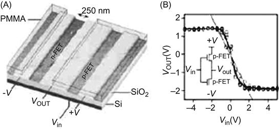
As shown in Figure 3.17C, an SWNT is first placed on Au electrodes deposited on an SiO2 layer, with the Si substrate being the gate electrode. This constitutes a 2-p-type CNT FET (the experiment is performed in a vacuum environment of less than 10−4 Pa at room temperature). Then, a polymethyl methacrylate (PMMA) photoresist is used to cover the CNT FET on the left side, while the right one is exposed in the vacuum for annealing. After that, the two CNT FETs are transformed into n type. The two annealed CNT FETs have Ids–Vg curves as shown in Figure 3.17A. The circuit is exposed to the 10−1 Pa oxygen environment for a certain time, the right CNT FET that is not protected with the PMMA returns to p type, and the CNT FET not covered by PMMA remains as n type. Here, Ids–Vg curves of the two CNT FETs become as shown in Figure 3.17B. This constitutes a CNT inverter, which works in exactly the same way as the ordinary complementary metal oxide semiconductor (CMOS) inverter, and its transmission characteristics are shown in Figure 3.17D.
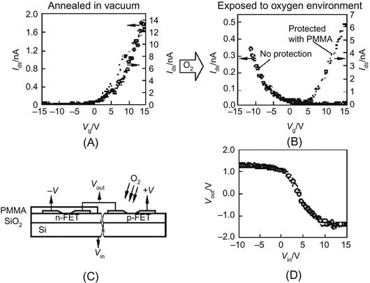
Figure 3.18A shows the AFM image of an inverter comprising a single nanotube on the three Au electrodes. Photoresist PMMA covers part of the CNT, with the other part being exposed. The exposed part of the CNT is doped with potassium, so that it becomes n type, whereas the part not covered by the PMMA remains p type. This also constitutes a CNT inverter. Figure 3.18B shows the equivalent inverter circuit and transmission characteristics. Its equivalent circuit can also be expressed as a CMOS circuit. When the input (Vin) is high (positive voltage), n-FET is turned on, and p-FET is off, the output (Vout) is low (negative voltage); when the input is low (positive voltage), p-FET is on, and n-FET is off, the output is high (negative voltage).
To summarize, the concepts and structures of some of the CNT-based logic circuits have been explained, but there are still many problems that remain unsolved. First, we must implement and verify all the logical elements of CNTs. For example, an important logical storage unit used to build DRAM (dynamic RAM) has not been realized. Previously described CNTs are mostly of the resistor–transistor logic, which is not a good logic style for current ICs. In principle, we expect to have complementary logic elements such as CMOS. Second, two key issues in the future that will constrain the development of CNT electronics need to be addressed: although the semiconductor-type and metallic CNTs can be screened when currently building devices and single-logic circuits, it is difficult to ensure the consistency of electrical properties of CNTs in large-scale production; and there are issues regarding positioning and manipulating massive amounts of CNTs in large-scale circuits. When these issues are resolved, CNT electronics will develop rapidly.
3.4.2 Other Applications of CNTs
The unique nature of CNTs provides an almost unlimited amount of potential applications, as discussed.
3.4.2.1 Nano Test Tubes
CNTs provide the smallest capillary to study capillarity mechanisms, and the smallest test tubes for chemists to perform chemical reactions.
3.4.2.2 Nanobalance
The microparticles on CNTs can cause changes of beat frequency of associated current. By taking advantage of this, scientists invented a “nanobalance,” with accuracy of 10−17 kg in 1999, which is able to weigh the quality of individual viruses. Further research on the nanobalance demonstrated that the weight of single atoms could be determined.
3.4.2.3 Nanomolds
Materials like metals and oxides can be filled inside CNTs, effectively using CNTs as molds. Specifically, the CNTs are first filled with metal and other materials, and then the carbon layer will be etched away. Thus, the smallest nanoscale wires or novel one-dimensional materials can be prepared and used in future molecular electronic devices or nanoelectronic devices.
3.4.2.4 CNTs: Field Emission Cathode Materials
Using CNTs as field emission cathode materials is expected to address problems limiting cathode-ray tubes.
The cathode field emitter in a display is made from silicon or metal and is usually processed by methods such as chemical etching and electron-beam deposition. Because of restrictions on microprocessing technology, the manufactured silicon or metal field emission device has a minimum size of approximately 20–50 nm with uniformity issues.
Field emission devices have a large maximum size, requiring their threshold voltage to reach 100 V or more to eject electrons. Such cathode field emission devices that have high operating voltages and inferior uniformity will not be applicable in the next generation of flat-panel displays.
CNTs provide an excellent choice for field emission cathode materials because the single-wall CNTs have an average diameter of 1–2 nm, only approximately one-tenth to one-twentieth of the maximum diameter of the silicon field emission cathode device that is widely used. The field emission cathode device made from SWNTs will be a very sharp and good electron emission source, with a threshold value of voltage for field emission that is able to be reduced to approximately 10 V, making it possible to produce a new generation of wall-mounted flat-panel displays with low energy consumption.
In 1999, Japan and South Korea successively developed CNT-based displays with thickness of a few centimeters. These products, compared with traditional displays, feature small size, light weight, good quality, low power consumption, fast dynamic response (only a few microseconds), and have a wide operating temperature range (able to work at a range of −45°C to +85°C). It is clear that CNTs may have great potential for application in flat-panel displays.
3.4.2.5 Application of CNTs in Hydrogen Storage
Hydrogen has been largely regarded as the future of clean energy. However, hydrogen itself is low in density, and compressing it into liquid is not convenient or safe. Lightweight CNTs with hollow structures can serve as an excellent hydrogen storage container, with a stored hydrogen density even higher than that of liquid or solid hydrogen. Through thermal control, the hydrogen inside can be slowly released and used as an energy source. Researchers are trying to use CNTs to produce lightweight and portable hydrogen storage containers.
As an absorption material with the largest hydrogen storage capacity, CNTs will also contribute to the development of hydrogen-fueled vehicles. The world’s four major automobile companies (General Motors, Ford, Toyota, and Daimler-Benz AG) are accelerating the development of hydrogen-fueled vehicles. For example, Toyota successfully developed the second-generation hydrogen fuel cell in March 2000, which is a novel solid polymer fuel cell using hydrogen as fuel. This car has an output power of up to 90 kW and maximum speed of 150 km/h, with the ability to be driven more than 300 km with one tank of hydrogen.
If we want to use hydrogen as a power source for vehicles, then some key conditions need to be met. A vehicle using hydrogen as fuel is expected to drive 500 km on 3.2 kg of hydrogen. This requires such vehicles to have containers with very large hydrogen storage density. Regarding two indicators of hydrogen storage, weight and volume, the container must, respectively, reach 6.5 wt% (weight percentage of hydrogen accounting for sum of hydrogen storage container and the hydrogen weight) and 62 kg H2/m3 (stored hydrogen weight per unit volume).
What is the future of CNT storage of hydrogen? The National Renewable Energy Laboratory and IBM performed a test of the ability of CNTs in adsorption of hydrogen (hydrogen storage capacity) in 1997 and found that the capacity of CNTs in adsorption of hydrogen increased as diameter increased. Thus, it is inferred that high-purity SWNTs have a hydrogen absorption capacity in the range of 5–10 wt%, of which the high-purity SWNTs with a diameter of 1.63–2.0 nm can attain hydrogen storage technical specifications of 6.5 wt%.
3.4.2.6 High-Energy Microbattery
With good electrical conductivity properties, CNTs can also serve as a cathode or supersede the conductive polymer material as a conductive medium to create high-energy batteries. These batteries feature a small size, high energy, and long life, and are the best choice for computers and automobiles.
3.4.2.7 High-Energy Capacitor
CNTs, after being pressed into sheets, can be used to make high-energy capacitors, whereas a small amount of CNTs added to other materials also can significantly improve the conductivity of the material (for example, polymer materials, by adding a certain amount of CNT, can make the resistivity lower by three orders of magnitude or more).
3.4.2.8 Chip Thermal/Heat Protection
With excellent thermal conductivity, CNTs are expected to become the heat plate for computer chips in the next generation of high-speed computers and can also be used as protective materials for a variety of high-temperature devices, such as engines and rockets.
3.4.2.9 Nanoreactor
Some researchers have also found that by virtue of a unique pore-like structure, large specific surface area (surface area per gram of CNTs up to several hundred square meters), and other characteristics, CNTs can be made into nanoreactors, which can make a chemical reaction confined to a small range.
3.4.2.10 Nanocomposite Materials
Based on the nature of CNTs, composite materials with high performance can be produced. For example, CNT-reinforced plastics have excellent mechanical properties, good conductivity, corrosion resistance, and the capacity to shield radio waves. The composite materials of CNTs with a cement matrix have good impact resistance as well as anti-static, anti-wear, highly stability, and environmentally friendly features. Ceramic composite materials, once reinforced with CNTs, can have high strength and good resistance to impact. The existence of the five-membered ring defects enhanced the reactivity of CNTs. Under the conditions of heat and the existence of other substances, CNTs tend to be at the end sides to form a tube, which is prone to metal infiltration to form metal matrix composite materials. Such materials, in addition to having high strength, high modulus, and high temperature, have very small thermal expansion coefficients and strong resistance to thermal changes.