
CHAPTER 2
GPRS/EDGE Handset Hardware
In this chapter we examine the hardware requirements for a GPRS tri-band phone capable of supporting higher-level modulation techniques. We address the design issues introduced by the need to produce the following:
A multislot handset. Capable of supporting GSM (8 slots) and US TDMA (3/6 slots)
A multiband handset. 800, 900, 1800, 1900 MHz
A multimode handset. Capable of processing constant envelope GMSK modulation (GSM) and higher-level modulation with AM components (US TDMA)
We need to combine these design requirements with an overall need to minimize component count and component cost. We also must avoid compromising RF performance.
Design Issues for a Multislot Phone
The idea of a multislot phone is that we can give a user more than one channel. For instance, one slot could be supporting a voice channel, other slots could be supporting separate but simultaneous data channels, and we can give a user a variable-rate channel. This means one 9.6 kbps channel (one slot) could be expanded to eight 9.6 kbps channels (76.8 kbps), or if less coding overhead was applied, one 14.4 kbps channel could be expanded to eight 14.4 kbps channels (115 kbps). Either option is generically described as bandwidth on demand.
In practice, the GSM interface was designed to work with a 1/8 duty cycle. Increasing the duty cycle increases the power budget (battery drain) and increases the need for heat dissipation. Additionally, multislotting may reduce the sensitivity of the handset, which effectively reduces the amount of downlink capacity available from the base station, and selectivity—a handset working on an 8-over-8 duty cycle creates more interference than a handset working on a 1-over-8 duty cycle).
The loss of sensitivity is because the time-division duplexing (time offset between transmit and receive) reduces or disappears as a consequence of the handset using multiple transmit slots. For certain types of GPRS phone this requires reinsertion of a duplex filter, with typically a 3 dB insertion loss, to separate transmit signal power at, say, +30 dBm from a receive signal at −102 dBm or below.
Revisiting the time slot arrangement for GSM shows how this happens (see Figure 2.1). The handset is active in one time slot—for example, time slot 2 will be used for transmit and receive. The transmit and receive frames are, however, offset by three time slots, resulting in a two time slot separation between transmit and receive. The time offset disappears when multiple transmit slots are used by the handset. An additional complication is that the handset has to measure the signal strength from its serving base station and up to five adjacent base stations. This is done on a frame-by-frame basis by using the six spare time slots (one per frame) to track round the beacon channels sent out by each of the six base stations. Multislotting results in rules that have hardware implications.
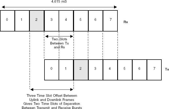
Figure 2.1 Time-division duplexing in GSM.
There are three classes of GPRS handset. Class A supports simultaneous GPRS and circuit-switched services—as well as SMS on the signaling channel—using a minimum of one time slot for each service. Class B does not support simultaneous GPRS and circuit-switched traffic. You can make or receive calls on either of the two services sequentially but not simultaneously. Class C is predefined at manufacture to be either GPRS or circuit-switched. There are then 29 (!) multislot classes.
For the sake of clarity we will use as examples just a few of the GPRS multislot options (see Table 2.1): Class 2 (two receive slots, one transmit), Class 4 (three receive slots, one transmit), Class 8 (four receive slots, one transmit), Class 10 (four receive slots, two transmit), Class 12 (four receive slots, four transmit), and as a possible longterm option, Class 18 (up to eight slots in both directions).
The maximum number of time slots Rx/Tx is fairly self-explanatory. A Class 4 handset can receive three time slots and transmit one. A Class 10 handset can receive up to four time slots and transmit up to two time slots, as long as the sum of uplink and downlink time slots does not exceed five.
The minimum number of time slots, shown in the right-hand column, describes the number of time slots needed by the handset to get ready to transmit after a receive slot or to get ready to receive after a transmit slot. This depends on whether or not the handset needs to do adjacent cell measurements. For example, Tta assumes adjacent cell measurements are needed. For Class 4, it takes a minimum of three time slots to do the measurement and get ready to transmit. If no adjacent cell measurements are needed (Ttb), one time slot will do. Tra is the number of time slots needed to do adjacent cell measurements and get ready to receive. For Class 4, this is three time slots. If no adjacent cell measurements are needed (Trb), one slot will do.
The type column refers to the need for a duplex filter; Type 1 does not need a duplex filter, Type 2 does. In a Class 18 handset, you cannot do adjacent cell measurements, since you are transmitting and receiving in all time slots, and you do not have any time separation between transmit and receive slots—(hence, the need for the RF duplexer).


Figure 2.2 Rx/Tx offsets and the monitor channel (Rx/Tx channels shown with frequency hopping).
The uplink and downlink asymmetry can be implemented in various ways. For example, a one-slot or two-slot separation may be maintained between transmit and receive.
Rx and Tx slots may overlap, resulting in loss of sensitivity. In addition, traffic channels may be required to follow a hop sequence, across up to 64 RF 200 kHz channels but more often over 6 or 24 channels.
Figure 2.2 shows the traffic channels hopping from frame to frame and the adjacent cell monitoring being done in one spare time slot per frame. The base station beacon channel frequencies—that is, the monitor channels—do not hop. The transmit slot on the uplink may be moved closer to the Rx slot to take into account round-trip delay.
From a hardware perspective, the design issues of multislotting can therefore be summarized as:
- How to deal with the loss of sensitivity and selectivity introduced by multislotting (that is, improve Tx filtering for all handsets, add duplex filtering for Type 2)
- How to manage the increase in duty cycle (power budget and heat dissipation)
- How to manage the different power levels (slot by slot)
A user may be using different time slots for different services and the base station may require the handset to transmit at different power levels from slot to slot depending on the fading experienced on the channel (see Figure 2.3).

Figure 2.3 GPRS transmitter transition.
The design brief for a multislot phone is therefore:
- To find a way of maintaining or increasing sensitivity and selectivity without increasing cost or component count
- To find a way of improving power amplifier (PA) efficiency (to decrease the multislot power budget, decrease the amount of heat generated by the PA, or improve heat dissipation, or any combination of these)
- To provide a mechanism for increasing and decreasing power levels from slot to slot
Design Issues for a Multiband Phone
In Chapter 1 we described frequency allocations in the 800, 900, 1800, and 1900 MHz bands. For a handset to work transparently in Europe, the United States, and Asia, it is necessary to cover all bands (800 and 1900 MHz for the United States, 900 and 1800 MHz for Europe and Asia).
If we assume for the moment that we will be using the GSM air interface in all bands (we cover multimode in the next section), then we need to implement the frequencies and duplex spacings shown in Table 2.2.
Table 2.2 Frequency Bands and Duplex Spacing

Handset outputs for GSM 800 and 900 are a maximum 2 W. A phone working on a 1/8 duty cycle will be capable of producing an RF burst of up to 2 W, equivalent to a handset continuously transmitting at 250 mW. Multislotting increases the power budget proportionately. Power outputs for GSM 1800 and 1900 are a maximum 1 W. A phone working on a 1/8 duty cycle is capable of producing an RF burst of 1 W, equivalent to a handset continuously transmitting a maximum of 125 mW.
The handsets need to be capable of accessing any one of 995 × 200 kHz Rx or Tx channels at a duplex spacing of 45, 80, or 95 MHz across a frequency range of 824 to 1990 MHz. Present implementations address GSM 900 and 1800 (for Europe and Asia) and GSM 1900 (for the United States). GSM 800, however, needs to be accommodated, if possible, within the design architecture to support GSM GPRS EDGE phones that are GAIT-compliant (GAIT is the standards group working on GSM ANSI Terminals capable of accessing a GSM-MAP network) and ANSI 41 (US TDMA) networks.
The design brief is to produce a tri-band (900/1800/1900) or quad band (800/900/1800/1900) phone delivering good sensitivity and selectivity across all channels in all (three or four) bands while maintaining or reducing RF component cost and component count.
Design Issues for a Multimode Phone
In addition to supporting multiple frequency bands, there is a perceived—and actual—market need to accommodate multiple modulation and multiplexing techniques. In other words, the designer needs to ensure a handset is capable of modulating and demodulating GSM GMSK (a two-level constant envelope modulation technique), GSM EDGE (8 level PSK, a modulation technique with amplitude components), π/4DQPSK (the four-level modulation technique used in US TDMA) and possibly, QPSK, the four-level modulation technique used on US CDMA. GMSK only needs a Class C amplifier, while eight-level PSK, π/4DQPSK, and QPSK all require substantially more linearity. (If AM components pass through a nonlinear amplifier, spectral regrowth occurs; that is, sidebands are generated.)
Implicitly this means using Class A/B amplifiers (20 to 30 percent efficient) rather than Class C amplifiers (50 to 60 percent efficient), which increases the power budget problem and heat dissipation issue. Alternatively, amplifiers need to be run as Class C when processing GMSK, Class A/B when processing nonconstant envelope modulation, or some form of baseband predistortion has to be introduced so that the RF platform becomes modulation-transparent. (RF efficiency is maintained but baseband processor overheads increase.)
The Design Brief for a Multislot, Multiband, Multimode Phone
We can now summarize the design objectives for a GSM multislot GPRS phone capable of working in several (three or four) frequency bands and capable of supporting other modulation techniques, such as non-constant envelope, and multiplexing (TDMA or CDMA) options.
- Design an architecture capable of receiving and generating discrete frequencies across four frequency bands (a total of 995 × 200 kHz channels) at duplex spacings of 45, 80, or 95 MHz while maintaining good frequency and phase stability. To maintain sensitivity, all handsets must be capable of frequency hopping from frame to frame (217 times a second).
- Maintain or improve sensitivity and selectivity without increasing component count or cost.
Multislot Design Objectives:
- Manage the increase in duty cycle and improve heat dissipation.
- Manage power-level differences slot to slot.
Multimode Design Objectives:
- Find some way of delivering power efficiency and linearity to accommodate non-constant envelope modulation.
As always, there is no single optimum solution but a number of options with relative merits and demerits and cost/performance/complexity trade-offs.
Receiver Architectures for Multiband/Multimode
The traditional receiver architecture of choice has been, and in many instances continues to be, the superheterodyne, or “superhet.” The principle of the superhet, invented by Edwin Armstrong early in the twentieth century, is to take the incoming received signal and to convert it, together with its modulation, down to a lower frequency—the intermediate frequency (IF), where channel selective filtering and most of the gain is performed. This selected, gained up channel is then demodulated to recover the baseband signal.
Because of the limited bandwidth and dynamic range performance of the superhet stages prior to downconversion, it is necessary to limit the receiver front-end bandwidth. Thus, the antenna performance is optimized across the band of choice, preselect filters have a similar bandwidth of design, and the performance and matching efficiencies of the low-noise amplifier (LNA) and mixer are similarly tailored.
For GSM GPRS, the handset preselect filters have a bandwidth of 25 MHz (GSM800), 39 MHz (GSM900), 75 MHz (GSM1800), or 60 MHz (GSM1900). The filter is used to limit the RF energy to only that in the bandwidth of interest in order to minimize the risk of overloading subsequent active stages. This filter may be part of the duplex filter. After amplification by the LNA, the signal is then mixed with the local oscillator (LO) to produce a difference frequency—the IF. The IF will be determined by the image frequency positioning, the selectivity capability and availability of the IF filter, and the required LO frequency and range.
The objective of the superhet is to move the signal to a low-cost, small form factor processing environment. The preselect filter and LNA have sufficient bandwidth to process all possible channels in the chosen band. This bandwidth is maintained to the input to the mixer, and the output from the mixer will also be wideband. Thus, a filter bandwidth of just one channel is needed to select, or pass, the required channel and reject all adjacent and nearby channels after the mixer stage. This filter is placed in the IF. In designing the superhet, the engineer has chosen the IF and either designed or selected an IF filter from a manufacturer's catalog.
The IF filter has traditionally had a bandwidth equal to the modulation bandwidth (plus practical tolerance margin) of a single channel. Because the output from the mixer is wideband to support multiple channels, it is necessary to position the wanted signal to pass through the selective IF filter. For example, if the IF filter had a center frequency of 150 MHz and the wanted channel was at 922 MHz, the LO would be set to 1072 MHz (1072-922 = 150 MHz) or 772 MHz (922-772 = 150 MHz) to translate the center of the wanted channel to the center of the IF filter. The designer must ensure that the passband of the filter can pass the modulation bandwidth without distortion. Following the selective filtering, the signal passes to the demodulator where the carrier (IF) is removed to leave the original baseband signal as sourced in the transmitter.
The IF filter and often the demodulator have traditionally been realized as electromechanical components utilizing piezoelectric material—ceramic, quartz, and so on. This approach has provided sufficient selectivity and quality of filtering for most lower-level (constant envelope) modulations, such as FM, FSK, and GMSK. However, with the move toward more complex modulation, such as π/4DQPSK, QPSK, and QAM, the performance—particularly the phase accuracy of this filter technology—produces distortion of the signal.
The second problem with this type of filter is that the parameters—center frequency, bandwidth, response shape, group delay, and so on—are fixed. The engineer is designing a receiver suitable for only one standard, for example, AMPS at 25 kHz bandwidth, IS136 at 30 kHz, GSM at 200 kHz. Using this fixed IF to tune the receiver, the LO must be stepped in channel increments to bring the desired channel into the IF.
Given the requirement for multimode phones modes with different modulation bandwidths and types, this fixed single-mode approach cannot be used. The solution is either to use multiple switched filters and demodulators or to adopt an alternative flexible approach.
The multi-filter approach increases the cost and form factor for every additional mode or standard added to the phone and does not overcome the problems of insufficient phase/delay performance in this selective component. A more cost-effective, flexible approach must be adopted.
It is the adoption of increasingly capable digital processing technology at an acceptable cost and power budget that is providing a flexible design solution. To utilize digital processes, it is necessary to convert the signal from the analog domain to the digital domain.
It would be ideal to convert the incoming RF to the digital domain and perform all receive processes in programmable logic. The ultimate approach would be to convert the whole of the cellular RF spectrum (400 MHz to 2500 MHz) in this way and to have all standards/modes/bands available in a common hardware platform—the so-called software radio. The capability to convert signals directly at RF—either narrowband or wideband—to the digital domain does not yet exist. The most advanced analog-to-digital converters (ADCs) cannot yet come near to this target. To configure a practical cost effective receiver, the ADC is positioned to sample and digitize the IF; that is, the conventional downconverting receiver front end is retained.
The receiver design engineer must decide the IF frequency and the IF bandwidth to be converted. In the superhet architecture, the higher the IF that can be used, the easier the design of the receiver front end. However, the higher the frequency to be converted, the higher the ADC power requirement.
If an IF bandwidth encompassing all channels in the band selected could be digitized, the receiver front end could be a simple non-tuning downconverter with channel selection being a digital baseband function. This is a viable technique for base station receivers where power consumption is less of an issue; however, for handsets, the ADC and DSP power required restricts the approach to digitization of a single-channel bandwidth.
This then returns us to single-channel passband filtering in the analog IF prior to digitization—a less than ideal approach for minimum component multimode handsets. However, minimum performance IF filters could be employed with phase compensation characteristics programmed into the digital baseband filtering to achieve overall suitability of performance.
Another possible approach is to use a single IF selective filter but with a bandwidth suitable for the widest mode/standard to be used. For W-CDMA, this would be 5 MHz. The 5 MHz bandwidth would then be digitized. If it was required to work in GSM mode, the required 200 kHz bandwidth could be produced in a digital filter. This approach needs careful evaluation. If the phone is working predominantly in GSM mode, the sampling/digitizing process is always working at a 5 MHz bandwidth. This will consume considerably more power than a sampling system dimensioned for 200 kHz.
So, in summary, the base station may use a wideband downconverter front end and sampling system with baseband channel tuning, but the handset will use a tunable front end with single-channel sampling and digital demodulation. The required number of converter bits must also be considered.
Again, the power consumption will be a key-limiting parameter, given the issues of input (IF) frequency and conversion bandwidth. The number of bits (resolution) equates directly to the ADC conversion or quantization noise produced, and this must be small compared with the carrier-to-noise ratio (CNR) of the signal to be converted. In a GSM/GPRS receiver, 8 to 10 bits may be necessary. In a W-CDMA receiver, since the IF CNR is considerably worse (because of the wideband noise created signal), 6 or even 4 bits may be sufficient.
In a mobile environment, the received signal strength can vary by at least 100 dB, and if this variability is to be digitized, an ADC of 20 bits plus would be required. Again, at the required sample rates this is impractical—the dynamic range of the signal applied to the ADC must be reduced. This reduction in dynamic range is achieved by the use of a variable-gain amplifier (VGA) before the ADC. Part of the digital processing function is to estimate the received signal strength and to use the result to increase or decrease the gain prior to the ADC.
This process can be applied quite heavily in the handset, since it is required to receive only one signal. However, in the base station, it is required to receive strong and weak signals simultaneously, so dynamic range control is less applicable. In 3G networks, aggressive power control also assists in this process. We consider further issues of the IF sampled superhet in node B design discussions in Chapter 11.
Direct Conversion Receivers
In this section we consider an alternative architecture to the superhet—the direct conversion receiver (DCR). Direct conversion receivers, also referred to as zero IF (ZIF), were first used in amateur radio in the 1950s, then HF receivers in the 1960s and 1970s, VHF pagers in the 1980s, 900 MHz/1800 MHz cordless and (some) cellular phones in the 1990s, and in GPRS and 3G designs today.
The superhet is a well-tried and -tested approach to receiver implementation, having good performance for most applications. However, it does have some disadvantages:
- It requires either additional front-end filters or a complex image reject mixer to prevent it from receiving two frequencies simultaneously—the wanted frequency and an unwanted frequency (the image frequency).
- If multiple bandwidths are to be received, multiple IF filters may be required.
- The digital sampling and conversion is performed at IF and so will require functions to work at these frequencies—this can require considerable current as the design frequency increases.
The DCR is directed at overcoming these problems. The principle is to inject the LO at a frequency equal to the received signal frequency. For example, if a channel at 920 MHz was to be received, the LO would be injected into the mixer at 920 MHz.
The mixer would perform the same function as in the superhet and output the difference of the signal and the LO. The output of the mixer, therefore, is a signal centered on 0 Hz (DC) with a bandwidth equal to the original modulation bandwidth. This brings in the concept of negative frequency (see Figure 2.4).
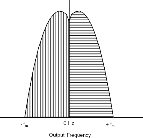
Figure 2.4 The negative frequency.
If the signal is obtained simply as the output of the mixer, it is seen as a conventional positive-only frequency where the lower sideband has been folded onto the upper sideband—the energies of the two sidebands are inseparable. To maintain and recover the total signal content (upper and lower sidebands), the signal must be represented in terms of its phase components.
To represent the signal by its phase components, it is necessary to perform a transform (Hilbert) on the incoming signal. This is achieved by splitting the signal and feeding it to two mixers that are fed with sine and cosine LO signals. In this way an in-phase (I) and quadrature phase (Q) representation of the signal (at baseband) is constructed. The accuracy or quality of the signal representation is dependent on the I and Q arm balance and the linearity of the total front end processing (see Figure 2.5).
Linearity of the receiver and spurious free generation of the LO is important, since intermodulation and distortion products will fall at DC, in the center of the recovered signal, unlike the superhet where such products will fall outside the IF. Second-order distortion will rectify the envelope of an amplitude modulated signal—for example, QPSK, π/4DQPSK, and so on to produce spurious baseband spectral energy centered at DC. This then adds to the desired downconverted signal.
It is particularly serious if the energy is that of a large unwanted signal lying in the receiver passband. The solution is to use balanced circuits in the RF front end, particularly the mixer, although a balanced LNA configuration will also assist (see Figure 2.6).


Figure 2.6 Even harmonic distortion.
If the balancing is optimum, even order products will be suppressed and only odd products created. However, even in a balanced circuit, the third harmonic of the desired signal may downconvert the third LO overtone to create spurious DC energy, adding to the fundamental downconverted signal. In the superhet, this downcon-verted component lies in the stopband of the IF filter.
Although the even and odd order terms may themselves be small, if the same intermodulation performance as the superhet is to be achieved, the linearities must be superior. As circuit balance improves, the most severe problem remaining is that of DC offsets in the stages following the mixer. DC offsets will occur in the middle of the downcon-verted spectrum, and if the baseband signal contains energy at DC (or near DC) distortions/offsets will degrade the signal quality, and SNR will be unacceptably low.
The problem can have several causes:
- Transistor mismatch in the signal path between the mixer and the I and Q inputs to the detector.
- The LO, passing back through the front end circuits (as it is on-frequency) and radiating from the antenna then reflects from a local object and reenters the receiver. The re-entrant signal then mixes with the LO, and DC terms are produced in the mixer (since sin2 and cos2 functions yield DC terms).
- A large incoming signal may leak into the LO port of the mixer and as in the previous condition self convert to DC.
The second and third problems can be particularly challenging, since their magnitude changes with receiver position and orientation.
DCRs were originally applied to pagers using two-tone FSK modulation. In this application DC offsets were not a problem because no energy existed around DC—the tones were + and −4.5 kHz either side of the carrier. The I and Q outputs could be AC coupled to lose the DC offsets without removing significant signal energy.
In the case of GSM/GPRS and QPSK, the problem is much more acute, as signal energy peaks to DC. After downconversion of the received signal to zero IF, these offsets will directly add to the peak of the spectrum. It is no longer possible to null offsets by capacitive coupling of the baseband signal path, because energy will be lost from the spectral peak. In a 200 kHz bandwidth channel with a bit error rate (BER) requirement of 10−3, a 5 Hz notch causes approximately 0.2 dB loss of sensitivity. A 20 Hz notch will stop the receiver working altogether.
It is necessary to measure or estimate the DC offsets and to remove (subtract) them. This can be done as a production test step for the fixed or nonvariable offsets, with compensating levels programmed into the digital baseband processing. Removing the signal-induced variable offsets is more complex. An example approach would be to average the signal level of the digitized baseband signal over a programmable time window. The time averaging is a critical parameter to be controlled in order to differentiate dynamic amplitude changes that result from propagation effects and changes caused by network effects, power control, traffic content, and so on.
Analog (RF) performance depends primarily on circuit linearity usually achieved at device level; however, this is a demanding approach both in power and complexity, and compensation at system level should be attempted. Baseband compensation is generally achieved as part of the digital signal processing and hence more easily achieved. Using a basic DCR configuration, control and compensation options may be considered (see Figure 2.7).
Receiver gain must be set to feed the received signal linearly to the ADC over an 80-to 90-dB range. Saturation in the LPF, as well as other stages, will unacceptably degrade a linear modulation signal—for example, QPSK, QAM, and π/4DQPSK. To avoid this problem, gain control in the RF and baseband linear front-end stages is employed, including the amplifier, mixer, and baseband amplifiers.
The front-end filter, or preselector, is still used to limit the RF bandwidth energy to the LNA and mixers, although since there is now no image, no other RF filters are required. Selectivity is achieved by use of lowpass filters in the I and Q arms, and these may be analog (prior to digital conversion) or digital (post digital conversion). The principle receive signal gain is now in the IQ arms at baseband, which can create the difficulty of high low-frequency noise, caused by flicker effects or 1/f.
Another increasingly popular method of addressing the classic DCR problems is to use a low IF or near-zero IF configuration. Instead of injecting the LO on a channel, it is set to a small offset frequency. The offset is design-dependent, but a one- or two-channel offset can be used or even a noninteger offset. The low IF receiver has a frequency offset on the I and Q and so requires the baseband filter to have the positive frequency characteristic different from the negative frequency characteristic (note that conventional filter forms are symmetrical). This is the polyphase filter. As energy is shifted away from 0 Hz, AC coupling may again be used, thus removing or blocking DC offsets and low-frequency flicker noise.
This solution works well if the adjacent channel levels are not too much higher than the wanted signal, since polyphase filter rejection is typically 30 to 40 dB.

Figure 2.7 Direct conversion receiver control and compensation circuits.
To Sum Up
Direct conversion receivers provide an elegant way of reducing component count, and component cost and increased use of baseband processing have meant that DCR can be applied to GPRS phones, including multiband, multimode GPRS. Careful impedance matching and attention to design detail means that some of the sensitivity and selectivity losses implicit in GPRS multislotting can be offset to deliver acceptable RF performance. Near-zero IF receivers, typically with an IF of 100 kHz (half-channel spacing) allow AC coupling to be used but require a more highly specified ADC.
Transmitter Architectures: Present Options
We identified in Chapter 1 a number of modulation techniques, including GMSK for GSM, π/4DQPSK for IS54 TDMA, 8 PSK for EDGE, and 16-level QAM for CDMA2000 1 × EV To provide some design standardization, modulation is usually achieved through a vector IQ modulator. This can manage all modulation types, and it separates the modulation process from the phase lock loop synthesizer—the function used to generate specific channel frequencies.

Figure 2.8 Upconverting transmitter.
As in the case of the superhet receiver, the traditional transmitter architecture has consisted of one or more upconversion stages from the frequency generating/modulating stage to the final PA. This approach allows a large part of the signal processing, amplification, filtering, and modulation to be performed at lower, cost-effective, highly integrated stages (see Figure 2.8). The design approach is low risk with a reasonably high performance.
The disadvantage of this approach is that a large number of unwanted frequencies are produced, including images and spurii, necessitating a correspondingly large number of filters. If multiband/multimode is the objective, the number of components can rise rapidly. Image reject mixers can help but will not remove the filters entirely. A typical configuration might use an on-chip IF filter and high local oscillator injection. With careful circuit design, it may be possible, where transmit and receive do not happen simultaneously, to reduce the number of filters by commoning the transmit and receive IFs.
Issues to Resolve
One problem with the architectures considered so far is that the final frequency is generated at the start of the transmitter chain and then gained up through relatively (tens of MHz) wideband stages. The consequence of this is to cause wideband noise to be present at the transmitter output stage—unless filters are inserted to remove it. The noise will be a particular problem out at the receive frequency, a duplex spacing away. (This noise will radiate and desensitize adjacent handsets ).
To attenuate the far out noise, filters must be added before and after the PA, and so the duplex filter has been retained. Again, in a multiband design this can increase the number of filters considerably.
To remove the need for these filters, an architecture called the offset loop or translational loop transmitter has been developed. This relies on using the noise-reducing bandwidth properties of the PLL. Essentially the PLL function is moved from the start of the transmitter to the output end, where the noise bandwidth becomes directly a function of the PLL bandwidth.
In a well-designed, well-characterized PLL, the wideband noise output is low. If the PLL can be implemented without a large divider ratio (N) in the loop, then the noise output can be reduced further. If such a loop is used directly in the back end of the transmitter, then the filters are not required.
A typical configuration will have a VCO running at the final frequency within a PLL. To translate the output frequency down to a reference frequency, a second PLL is mixed into the primary loop. Tuning is accomplished by tuning the secondary loop, and in this example, modulation is applied to the sampling frequency process. If there are no dividers, modulation transfer is transparent. A number of critical RF components are still needed, however. For example, the tuning and modulation oscillators require resonators, and 1800 MHz channels need to be produced by a doubler or band-switched resonators.
Figure 2.9 shows a similar configuration, but using dividers, for a multiband implementation (single-band, dual-band, or tri-band GSM). Modulation is applied to a PLL with the VCO running at final frequency. Again, this reduces wideband noise sufficiently to allow the duplex filter to be replaced with a switch. Because of the lack of up-conversion, there are no image products, so no output bandpass filters are required.
The advantage of this implementation is that it reduces losses between the transmit power amplifier and the antenna and allows the RF power amplifier to be driven into saturation without signal degradation. The loop attempts to track out the modulation, which is introduced as a phase error and so transfers the modulation onto the final frequency Tx VCO. Channel selection is achieved by tuning the offset oscillator, which doubles as the first local oscillator in receive mode.

Figure 2.9 Multiband GSM 900/1800/1900 MHz.
There are a number of implementation challenges in an OPLL design:
- The noise transmitted in the receive band and modulation accuracy is determined by the closed-loop performance of the OPLL. If the loop bandwidth is too narrow, modulation accuracy is degraded; if the loop bandwidth is too wide, the receive band noise floor rises.
- Because the OPLL processes phase and can only respond to phase lock functions for modulation, an OPLL design is unable to handle modulation types that have amplitude components. Thus, it has only been applied to constant envelope modulations (for example, FM, FSK, and GMSK).
- Design work is proceeding to apply the benefits of the OPLL to non-constant envelope modulation to make the architecture suitable for EDGE and QPSK. Approaches depend mainly on using the amplitude limiting characteristics of the PLL to remove the amplitude changes but to modulate correctly the phase components and then to remodulate the AM components back onto the PA output.
With the above options, the advantage of having a simple output duplex switch (usually a GaAs device) is only available when nonsimultaneous transmit/receive is used. When higher-level GPRS classes are used, the duplex filter must be reinstated.
A number of vendors are looking at alternative ways to manage the amplitude and phase components in the signal path. For illustration purposes, we'll look at an example from Tropian (www.tropian.com). The Tropian implementation uses a core modulator in which the amplitude and phase paths are synchronized digitally to control timing alignment and modulation accuracy (see Figure 2.10). The digital phase and amplitude modulator is implemented in CMOS and the RF PA in GaAs MOSFET.
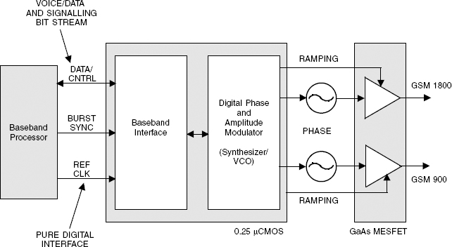
Figure 2.10 Tropian transmitter handset system block diagram.
We revisit linearization and adaptive predistortion techniques again when we study base station hardware implementation in Chapter 11. In the last part of this chapter we focus on the remaining design brief areas for achieving a multiband, multislot, multimode handset.
GPRS RF PA
There are two particular issues with GPRS RF PA design:
- The duty cycle can change from 1/8 to 8/8.
- Power levels can change between time slots.
The need to improve power efficiency focuses a substantial amount of R&D effort on RF materials. Table 2.3 compares present options on the basis of maturity, cost per Watt, whether or not the processes need a negative voltage, and power-added efficiencies at 900/1800 MHz.
Given that power-added efficiencies better than 55 percent are very hard to achieve in practice (even with Class C amplifiers), heat dissipation is a critical issue and has led to the increased use of copper substrates to improve conductivity. Recently, silicon germanium has grown in popularity as a material for use at 1800 MHz/2 GHz, giving efficient gain and noise performance at relatively low cost.
Implementing multislot GPRS with modulation techniques that contain amplitude components will be substantially harder to achieve—for example, the (4DQPSK modulation used in IS54TDMA or the eight-level PSK used in EDGE.
Table 2.3 Device Technology Comparison

In a practical phone design, linearity is always traded against DC power consumption. Factors that decide the final position on this linearity/efficiency trade-off include the following:
- The semiconductor material, Si, GaAs, SiGe, and so on
- The transistor construction, packaging technique, bond wire inductances, and so on
- The number of components used in and around the power amplifiers
- The expertise and capability of the design engineer
Designers have the option of using discrete devices, an integrated PA, or a module. To operate at a practical power efficiency/linearity level, there will inevitably be a degree of nonlinearity in the PA stage. This in turn makes the characterization of the parameters that influence efficiency and linearity difficult to measure and difficult to model. Most optimization of efficiency is carried out by a number of empirical processes (for example, load line characterization, load pull analysis, and harmonic shorting methods).
Results are not always obvious—for instance, networks matching the PA output to 50 ohms are frequently configured as a lowpass filter that attenuates the nonlinearities generated in the output device. The PA appears to have a good—that is, low—harmonic performance. The nonlinearity becomes evident when a non-constant envelope (modulated) signal is applied to the PA as intermodulation products and spectral spreading are seen.
Until recently the RF PA was the only function in a 2 GHz mobile phone where efficiency and linearity arguments favored GaAs over silicon. The situation is changing. Advances in both silicon (Si) and silicon germanium (SiGe) processes, especially in 3G phone development, make these materials strong contenders in new designs.
Higher performance is only obtained through attention to careful design. Advanced design techniques require advanced modeling/simulation to obtain the potential benefits. Design implementation is still the major cause of disappointing performance. In Chapter 11 we examine GPRS base station and 3G Node B design, including linearization techniques, power matching, and related performance optimization techniques.
Manage Power-Level Difference Slot to Slot
The power levels and power masks are described in GSM 11.10-1. Compliance requires the first time slot be set to maximum power (PMAX) and the second time slot to minimum power, with all subsequent slots set to maximum. PMAX is a variable established by the base station and establishes the maximum power allowed for handset transmit. The handset uses received power measurements to calculate a second value and transmits with the lower one.
This open-loop control requires a close, accurate link between received signal and transmitted power, which in turn requires careful calibration and testing during production. All TDMA transmissions (handset to base, base to handset) require transmit burst shaping and power control to maintain RF energy within the allocated time slot. The simplest form of power control is to use an adjustable gain element in the transmitter amplifying chain. Either an in-line attenuator is used (for example, PIN diode), a variable gain driver amplifier, or power rail control on the final PA.
The principal problem with this open-loop power control is the large number of unknowns that determine the output power—for example, device gains, temperature, variable loading conditions, and variable drive levels. To overcome some of the problems in the open-loop system, a closed-loop feedback may be used.
The power leveling/controlling of RF power amplifiers (transmitter output stages) is performed by tapping off a small amount of the RF output power, feeding it to a diode detector (producing a DC proportional to the RF energy detected), comparing the DC obtained with a reference level (variable if required), and using the comparison output to control the PA and PA driver chain gain.
RF output power control can be implemented using a closed-loop approach. The RF power is sampled at the output using a directional coupler or capacitive divider and is detected in a fast Schottky diode. The resultant signal representing the peak RF output voltage is compared to a reference voltage in an error amplifier. The loop controls the power amplifier gain via a control line to force the measured voltage and the reference voltage to be equal.
Power control is accomplished by changing the reference voltage. Although straightforward as a technique, there are disadvantages:
- The diode temperature variation requires compensation to achieve the required accuracy. The dynamic range is limited to that of the detector diode (approximately 20 dB—without compensation).
- Loop gain can vary significantly over the dynamic range, causing stability problems.
- Switching transients are difficult to control if loop bandwidth is not constant.
An alternative control mechanism can be used with amplifiers employing square law devices (for example, FETs). The supply voltage can be used to control the amplifier's output power. The RF output power from an amplifier is proportional to the square of the supply voltage. Reducing the drain voltage effectively limits the RF voltage swing and, hence, limits the output power. The response time for this technique is very fast, and in the case of a square-law device, this response time is voltage-linear, for a constant load.
The direct diode detection power control system has been satisfactory for analog cellular systems and is just satisfactory for current TDMA cellular systems (for example, GSM, IS54 TDMA, and PDC), although as voltage headrooms come down (4.8 V to 3.3 V to 2.7 V), lossy supply control becomes unacceptable.
CDMA and W-CDMA require the transmitter power to be controlled more accurately and more frequently than previous systems. This has driven R&D to find power control methods that meet the new requirements and are more production-cost-effective.
Analog Devices, for example, have an application specific IC that replaces the traditional simple diode detector with an active logarithmic detector. The feedback includes a variable gain single pole low pass filter with the gain determined by a multiplying digital-to-analog converter (DAC) The ADC is removed. A switched RF attenuator is added between the output coupler and the detector, and a voltage reference source is added. Power control is achieved by selecting/deselecting the RF attenuator and adjusting the gain of the LPF by means of the DAC
The system relies on the use of detecting log amps that work at RF to allow direct measurement of the transmitted signal strength over a wide dynamic range. Detecting log amps have a considerable application history in wide dynamic range signal measurement—for example, spectrum analyzers. Recently the implementation has improved and higher accuracy now results from improvements in their key parameters: slope and intercept.
Power Amplifier Summary
TDMA systems have always required close control of burst shaping—the rise and fall of the power envelope either side of the slot burst.
In GPRS this process has to be implemented on multiple slots with significant variations in power from burst to burst. Log detector power control implementations improve the level of control available and provide forward compatibility with 3G handset requirements.
Multiband Frequency Generation
Consider that the requirement is to design an architecture capable of generating discrete frequencies across four frequency bands (a total of 995 × 200 kHz channels) at duplex spacings of 45, 80, and 95 MHz while maintaining good frequency and phase stability.
The system block used in cellular handsets (and prior generations of two-way radios) to generate specific frequencies at specific channel spacings is the frequency synthesizer—the process is described as frequency synthesis. PLLs have been the dominant approach to RF frequency synthesis through 1G and 2G systems and will continue to be the technology of choice for RF signal generation in 2.5G and 3G applications.
The synthesizer is required to generate frequencies across the required range, increment in channel sized steps, move rapidly from one channel to another (support frequency hopping and handover), and have a low-noise, distortion-free output.
In 1G systems the network protocols allowed tens of milliseconds to shift between channels—a simple task for the PLL. PLLs were traditionally implemented with relatively simple integer dividers in the feedback loop. This approach requires that the frequency/phase comparison frequency is equal to the minimum frequency step size (channel spacing) required. This in turn primarily dictated the loop filter time constant—that is, the PLL bandwidth and hence the settling time.
GSM has a channel spacing of 200 kHz, and so fREF is 200 kHz. But the GSM network required channel changes in hundreds of microseconds. With a reference of 200 kHz the channel switching rate cannot be met, so various speed-up techniques have been developed to cheat the time constant during frequency changes.
In parallel with this requirement, PLL techniques have been developed to enable RF signal generators and test synthesizers to obtain smaller step increments—without sacrificing other performance parameters. This technique was based on the ability to reconfigure the feedback divider to divide in sub-integer steps—the Fractional-N PLL. This had the advantage of increasing the reference by a number equal to the fractional division, for example:
Integer-N PLL
- O/P frequency = 932 MHz, fREF = 200 kHz
- N = 932 MHz/200 kHz = 4660
Fractional-N PLL
- If N can divide in 1/8ths, (that is, 0.125/0.250/0.375, etc.)
- O/P frequency = 932 MHz, fREF = 200 kHz × 8 = 1.6 MHz
- N = 932 MHz/1.6 MHz = 582.5
This should have two benefits:
- The noise generated by a PLL is primarily a function of the division ratio, so reducing N should give a cleaner output, for example:
Integer-N PLL
- N = 4660
- Noise = 20log4660
- = 73.4 dB
Fractional-N PLL
- N= 582.5
- Noise = 20log582.5
- = 55 dB
for an 18.4-dB improvement.
- As the reference frequency is now 1.6 MHz, the loop is much faster and so more easily meets the switching speed/settling time requirements. However, the cost is a considerable increase in the amount of digital steering and compensation logic that is required to enable the Fractional-N loop to perform. For this reason, in many implementations the benefit has been marginal (or even negative).
Interestingly, some vendors are again offering Integer-N loops for some of the more advanced applications (for example, GPRS and EDGE) and proposing either two loops—one changing and settling while the second is outputting—or using sophisticated speed-up techniques.
A typical example has three PLLs on chip complete with VCO transistor and varactors—resonators off chip. Two PLLs are for the 900 MHz and 1.8 GHz (PLL1) and 750 MHz to 1.5 GHz (PLL2). The third PLL is for the IF/demodulator function.
Summary
The introduction of GPRS has placed a number of new demands on handset designers. Multislotting has made it hard to maintain the year-on-year performance improvements that were delivered in the early years of GSM (performance improvements that came partly from production volume—the closer control of RF component parameters). This volume-related performance gain produced an average 1 dB per year of additional sensitivity between 1992 and 1997.
Smaller form factor handsets, tri-band phones, and more recently, multislot GPRS phones have together resulted in a decrease in handset sensitivity. In general, network density today is sufficient to ensure that this is not greatly noticed by the subscriber but does indicate that GSM (and related TDMA technologies) are nearing the end of their maturation cycle in terms of technology capability. The room for improvement reduces over time.
Present GPRS handsets typically support three or four time slots on the downlink and one time slot on the uplink, to avoid problem of overheating and RF power budget in the handset.
Good performance can still be achieved either by careful implementation of multiband-friendly direct conversion receiver architectures or superhet designs with digital IF processing. Handsets are typically dual-band (900/1800 MHz) or tri-band (900/1800/1900 MHz).
In the next chapter, we set out to review the hardware evolution needed to deliver third-generation handsets while maintaining backward compatibility with existing GSM, GPRS, and EDGE designs.