
5 Basic circuitry
The following sections focus on the basic circuitry used in AN/FSQ-7 – a necessary task for understanding and marveling the machine as such. While today’s abundant ultralarge scale integrated circuits280 easily contain hundreds of millions and even billions of active circuit elements in the form of transistors, a simplex AN/FSQ-7 had to make do with fewer than 30,000 vacuum tubes, resulting in a rather straightforward, yet quite powerful architecture for its time.
At first we will focus on the basic waveforms employed throughout the computer system, and a problem quite common in the era of AN/FSQ-7 and its solution will be detailed.
5.1 Introduction
Many of the circuits described in the following sections will look familiar to readers with some background in electronics, since most of the vacuum tubes used behave quite like junction field-effect transistors.281
Due to the sheer size of AN/FSQ-7, where cables were measured in meters, the circuit designers were confronted with the problem of parasitic oscillations in the computer circuits. Such oscillations must be avoided at all costs in a digital computer where even a single pulse transmits information. Figure 5.1 shows a very basic and nonsensical vacuum circuit on the left side, basically consisting of a single triode. This tube’s plate is connected to the positive supply voltage through resistor R1 while its cathode and grid are connected directly to ground. In an ideal world this configuration would be stable and the tube would not conduct much current due to the grid being at ground potential.
Although every reasonable circuit designer would strive to keep the supply and control leads of the active elements as short as possible, the sheer size of AN/FSQ-7 made this impossible. This size was dictated not only by the fact that vacuum tubes, generating a great amount of heat, were employed – a further complication was the requirement for utmost serviceability which resulted in a rather sparse packaging. Elements were grouped into pluggable modules which could be removed and replaced easily by maintenance personnel. All this added to the unavoidable length of the wiring which resulted in the formation of parasitic resonant circuits. The right hand side of figure 5.1 shows the same circuit as it results from these non-negligible lengths of interconnecting wires.

Figure 5.1: Parasitic inductances and capacitances in circuits
Between grid and ground, and plate and ground, two parasitic capacitances, C1 and C2, have to be taken into account, which are due to the construction of the vacuum tube itself. In addition to this, the long wires connecting the circuit to its supply and control voltages form unintended inductors L1 and L2. These two effects combined can and often will yield an unstable circuit which is subject to oscillations.
Mainly two techniques were employed in AN/FSQ-7 to suppress these oscillations: The first is to insert resistors into signal and power lines which are dimensioned in a way that the resonant circuit cannot oscillate due to the loss introduced by these resistors.282 The second method is based on RC-combinations, combinations of a resistor and a capacitor which act as simple low-pass filter circuits in the supply lines. These RC-combinations have a crucial role since many switching circuits are connected to the same supply voltages. Without simple filters like these, spikes caused by the process of switching of one element could affect other elements connected to the same supply lines.
As can be seen in all of the following practical circuits, these RC-combinations often consisted of a 220 Ω resistor and a 10 nF capacitor. The reactance XC of the capacitor is given by
where ƒ denotes the critical frequency at which decoupling in the circuit is required, while C represents the capacity. A typical value for ƒ in AN/FSQ-7 is 1 MHz, where a 10 nF capacitor exhibits a reactance of about 15.9 Ω. A signal of that frequency or an impulse of corresponding duration will now “see” the capacitor as a rather low resistance compared with the 220 Ω resistor of the RC-combination. Since the capacitor is connected to ground, it will effectively suppress that signal or pulse by providing a low-resistance ground path, thus decoupling the switching circuit from other circuits connected to the same power line.
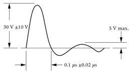
Figure 5.2: Standard pulse within AN/FSQ-7 (see [IBM BASIC CIRCUITS][p. 5])
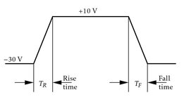
Figure 5.3: Standard levels within AN/FSQ-7 (see [IBM BASIC CIRCUITS] [p. 5])
Throughout AN/FSQ-7 two standard signals were used: A standard pulse and a standard level as shown in figures 5.2 and 5.3. The height of a standard pulse is about 30 V ± 10% while its width is 100 ns ±20 ns. These pulses were used to trigger various circuits like flip-flops etc. The other signal type is the standard level which is either at a potential of +10 V or at −30 V representing the two logical values of BOOLEan algebra.
The basic symbols used in the schematics of AN/FSQ-7 for circuit elements and signals are quite different from what we are used to seeing today. Figure 5.4 shows the four different arrows used to denote standard pulses and levels and their respective non-standard counterparts.283 These symbols are used to denote input as well as output lines of circuit elements.

Figure 5.4: Signal symbols denoting pulses and levels (see [IBM BASIC CIRCUITS][p. 5])
The following sections now focus on the operation of the basic circuit elements used in AN/FSQ-7. In cases where different implementations for similar functions like a flip-flop were used, only one particular or at most few variation have been selected exemplarily for discussion.284 Table 5.1 shows the basic circuit groups covered in the following sections. All basic building blocks can be grouped into logic and non-logic circuits which are then further detailed.

Table 5.1: Grouping of basic circuits (see [IBM BASIC CIRCUITS][p. 3])
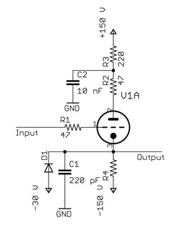
Figure 5.5: Basic schematic of a cathode follower (see [IBM BASIC CIRCUITS][p. 17])
5.2 Cathode follower
One of the most basic vacuum tube circuits of all is the cathode follower285 which has been introduced in section 2.2. Figure 5.5 shows the schematic of such a cathode follower as used in AN/FSQ-7. Due to its high-impedance input and low-impedance output, the cathode follower acts as a non-inverting amplifier with approximately unity gain and accordingly belongs to the power amplifier group.
The deviations of this circuit from the basic cathode follower shown in figure 2.4 are mostly due to the necessity of suppressing parasitic oscillations as described before: First of all, the input signal is connected to the control grid of the triode through a series resistor counteracting the inductance introduced by the input wiring. The RC-COMBINATION consisting of R3 and C2 in the plate circuit of the tube effectively suppresses spikes which could otherwise be coupled to other circuits through the +150 V supply line. The cathode is connected to −150 V through R4 with a diode clamping the output signal to −30 V at minimum. The actual value of R4 varies for different types of cathode followers. The AN/FSQ-7 used eight different variants with typical values of R4 between 17.1 kΩ and 40.1 kΩ or no R4 at all. The capacitor C1 decreases the fall time TF of the output signal, as it provides a low-resistance ground path for high frequency signals. TF is also affected by the size of R4 – the smaller this resistor, the shorter the fall time.
The abstract symbol for such a cathode follower is shown in figure 5.6. Input and output as denoted here are standard levels, and no particular variation of the circuit has been specified. A specific module will be denoted by a small capital letter B, C, D, E, F, G, H, or J to the left of “CF”.
Figure 5.6: Symbol of a cathode follower
5.3 Pulse amplifier
The second element of the power amplifier group is the pulse amplifier.286 This circuit amplifies a standard pulse so that a higher load can be driven. In modern parlance a pulse amplifier increases the fan-out of a signal. AN/FSQ-7 used three different models of this amplifier, denoted by A, B, and C. Type A can drive a constant light load of two to eight load units,287 type B is capable of driving a constant heavy load of five to eleven load units, while type C was used in case of varying light loads between zero and three units. The abstract symbol of a pulse amplifier is shown in figure 5.7. As its name implies, this circuit element requires and yields standard pulses instead of levels.
Figure 5.7: Symbol of a type A pulse amplifier (type B and C would be denoted by “BPA” and “CPA”, respectively)
Figure 5.8 shows a model A pulse amplifier for constant light load. At its heart is the pentode V1 which has its suppressor grid tied to a slightly positive voltage through the RC-combination R6 and C4, while its screen grid is at an even higher potential due to R5 and C3. The output circuit of this pulse amplifier consists of the transformer TO which inverts the polarity of the output pulse and serves as an impedance matching element for the elements connected to its secondary. Its turn ratio is 4:1 resulting in an impedance ratio of 16:1.
The control grid of V1 is biased at −15 V through R3 and R2 (C2 smoothes this bias voltage). The input signal is decoupled from this biased grid circuit through capacitor C1. An incoming standard pulse counteracts this negative grid bias so that V1 begins to conduct. The pulse current flowing through the pentode generates an output-pulse at the secondary of TO. The diode D1 creates a low-resistance discharge path for the input coupling capacitor C1. The resistor R1 terminates the input line to avoid reflection of pulses back to the generating circuit.

Figure 5.8: Type A pulse amplifier circuit (see [IBM BASIC CIRCUITS][p. 26])
The type B pulse amplifier is similar to this type A variant. The only difference concerns the suppressor grid which is tied to the plate by a 10 Ω resistor instead of being tied to the +90 V potential.288 The type C circuit is based on type B with a modified input network.
The input circuit shown in figure 5.8 is a so-called pulsed OR input while a slightly modified input network in which D1 is omitted and R2 is replaced by a resistor in series with a coil was called direct input.289
5.4 Register driver
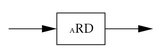
Figure 5.9: Symbol of a type A register driver (type B would be denoted by “BRD”)
The last element of the power amplifier group is the register driver,290 the symbol of which is shown in figure 5.9. Basically this device consists of several pulse amplifiers driven by a common input signal. Types A and B differ only marginally with respect to their input network. The detailed schematic of a type A register driver is shown in figure 5.10.

Figure 5.10: Register driver circuit (see [IBM BASIC CIRCUITS][p. 32])
The only difference with respect to a pulse amplifier is the input stage which decouples the input signal from the biased grids of the output stages by means of the transformer TI. The grids are biased at −30 V through R1, R2, and the secondary winding of TI. A standard pulse applied to the primary side of TI results in a positive pulse at its secondary, followed by a rather large negative undershoot due to resonance effects. This negative undershoot is limited by D1 and R3. The coil L1 in parallel to R1 helps suppressing the generation of a reflected signal at the primary of TI.
5.5 Relay drivers
The next section of the non-logic group contains two relay driver circuits, the thyratron relay driver291 and the vacuum tube relay driver.292 First of all the principle of operation of a thyratron should be explained:
A thyratron is essentially a gas-filled tube which can best be compared with today’s thyristors.293 The thyratrons used as relay drivers in AN/FSQ-7 were Xenon filled tetrodes, i. e. tubes with two grids, one control grid and one shield grid. In contrast to a vacuum tetrode, a positive potential at the control grid can be used to trigger the thyratron in such a way that a conducting path of ions is generated between plate and cathode of the thyratron. As a precondition, the potential difference between plate and cathode must match or exceed the ionization potential of the tube which is determined by various factors such as the tube’s geometry, the filling gas, and its pressure. When a thyratron is conducting, the control grid becomes ineffective due to a cloud of positively charged ions around it, so the only way to switch off a thyratron is to lower the plate-cathode potential difference to a level much lower than the ionization potential. This level is called the extinction potential of the tube.
Figure 5.11 shows the circuit of a model A thyratron relay driver:294 With the circuit breaker closed, the potential between plate and cathode is well above the necessary ionization potential. Since the control grid is negatively biased through R2 and R3, the tube will not conduct. A positive incoming pulse will raise the grid potential through the decoupling capacitor C3, thus triggering the thyratron. As a result of this, the current flowing through V1, R5 and the circuit breaker will activate the relay K1.295 To reset the relay driver, the circuit breaker must be opened either manually or automatically, so that the ionization potential is no longer maintained between plate and cathode. 296
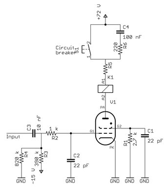
Figure 5.11: Basic form of a thyratron relay driver (see [IBM BASIC CIRCUITS][p. 36])
Figure 5.12 shows the abstract circuit symbol for such a type A thyratron relay driver.297 Due to the high amount of current a thyratron can switch, this type of driver was mainly used to drive multiple relays, print and punch magnets or wire contact relays.298
Figure 5.12: Symbol of a Type A thyratron relay driver
The symbol of a vacuum tube relay driver is shown in figure 5.13. Since the triodes used in this circuit (see figure 5.14) are not capable of driving currents as high as those of the thyratron circuit, typically only a single low-energy relay can be controlled by these drivers. Accordingly, the symbol incorporates the relay contacts.

Figure 5.13: Symbol of a vacuum tube relay driver
The circuit is quite straightforward: The triode V1A is controlled by a standard level applied to its grid through resistor R1. When the grid becomes sufficiently positive with respect to the cathode, i. e. at about +10 V, the tube begins to conduct and the current flowing from cathode to plate energizes relay K1 through R2 and R3. R3 and C2 form an RC-combination to make sure that no spikes from switching the relay will enter the supply rail. An additional means toward this is C1 which slows down the rise time of the grid voltage since the transition from −30 V to +10 V of the input signal must change the charge stored in this capacitor. This results in a slower rise of the current flowing through the relay. The same effect takes place when the input signal falls.
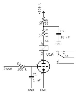
Figure 5.14: Basic form of a vacuum tube relay driver (see [IBM BASIC CIRCUITS][p. 39])
5.6 Level setter
The so-called level setter299 is a member of the restorer group of table 5.1. It employs a cathode follower as its output stage while the input circuit consists of another cathode follower driving a so-called grounded grid amplifier. The purpose of the level setter is to restore proper signal levels of an input signal. There are two types of this device: Model A accepts an input signal with a high-level between +12 V and 0 V and a low-level between −30 V and −8 V, while model B requires an input signal with a high-level between +12 V and +6 V and a low-level between -30 V and −11 V.
Figure 5.15: Symbol of a type A level setter (type B would be denoted by “BLA”)
Figure 5.15 shows the abstract symbol of a model A level setter as used in the AN/FSQ-7 schematics. Figure 5.16 shows the detailed schematic of a model A level setter.
The input stage cathode follower is dimensioned so that a negative input voltage connected through R1 to the grid results in a negative output voltage at the cathode of V1A. The grid of the second triode V1B is connected to a voltage divider consisting of resistors
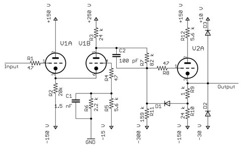
Figure 5.16: Type A level setter circuit (see [IBM BASIC CIRCUITS][p. 22])
R5 and R6, which is connected between the –15 V supply and ground. By means of this voltage divider, the grid is at a slightly negative fixed potential with respect to ground.
When the cathode potential of V1A becomes negative due to a negative input level, the cathode potential of V1B follows. As a result of this, the grid of V1B becomes positive with respect to its cathode and the tube begins to conduct. Thus the plate potential of V1B drops due to the current flowing through R3 and R2. Accordingly, the grid potential of the output stage triode V2A, which is connected to the voltage divider consisting of R7 and R11, becomes negative and the tube stops conducting and its cathode potential will become negative with respect to ground. Due to the clamping diode D2, the output of this last stage is limited to −30 V, the desired standard level potential.
In case of a positive input signal, things reverse: V1A conducts, so its cathode potential will become positive, making the cathode of V1B positive, too. The grid potential of V2A will then be negative with respect to its cathode and V2B does not conduct. As a result, the grid of V2A becomes positive with respect to its cathode and the triode will start to conduct. Its output will rise to a rather positive voltage which is clamped by D3 to +10 V.
The type B level setter differs from type A in various respects: First of all, the cathode of V1B is no longer connected to the cathode of V1A directly but through a voltage divider which replaces R2, thus effectively changing the input signal thresholds. Second, all positive supply voltages are decoupled by RC-combinations consisting of a 220 Ω resistor and a 10 nF capacitor to reduce injection of switching noise into the supply lines.

Figure 5.17: Basic two-input AND circuit (see [IBM BASIC CIRCUITS][p. 42])

Figure 5.18: Symbol of an AND circuit (see [IBM BASIC CIRCUITS][p. 41])
Figure 5.19: Basic two-input OR circuit (see [IBM BASIC CIRCUITS][p. 43])
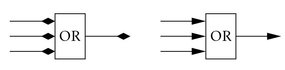
Figure 5.20: Symbol of an OR circuit (see [IBM BASIC CIRCUITS][p. 43])
5.7 Diode AND and OR circuits
Gates implementing logical AND and OR operations belong to the coincidence group of table 5.1 and are based on simple diode networks in AN/FSQ-7. Figures 5.17 and 5.18 show the schematic of a two-input AND gate as well as the abstract symbol for an AND circuit with three input lines.300 The principle of operation is simple: When at least one of the two inputs is at −30 V potential, it will tie the output down to this voltage. Only if both inputs are at +10 V, the output will go high.
In principle, the diode D3 would be unnecessary as it just acts as a third input to the AND gate that is always tied to +10 V. Its purpose is to protect following vacuum tube circuits from excessive grid levels301 in case of inputs to the AND gate being driven way beyond +10 V due to a component failure in an earlier stage. In this case, D3 clamps the output signal to +10 V.
OR gates were based on the same scheme but with reversed diodes and reversed bias voltage as shown in figure 5.19. Due to D3, the output voltage is clamped at a maximum negative voltage of −30 V. If both inputs are at −30 V a current will flow through D1 and D2 yielding −30 V at the output. If, e. g. diode D1 is at +10 V potential at its anode, a current will flow through it, effectively raising the output potential to +10 V, too. If the second input is still at −30 V, D2 will stop conducting since its cathode is now at a higher potential than its anode, thus a single input – more are possible by adding input diodes to this circuit – can force the output to +10 V potential.
The OR circuit exhibits a much faster signal rise time than the AND circuit due to the latter’s higher load capacitances. Accordingly, the OR circuit may be used with standard levels as well as standard pulses as inputs while the AND circuit works only with standard levels. Figure 5.20 shows both variations of the abstract symbol for a three-input OR circuit, the (standard level) diode OR and the pulsed OR.
5.8 Gate tube circuit
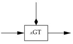
Figure 5.21: Symbol of a model A gate tube
The gate tube circuit302 is part of the logical elements of table 5.1. It implements a coincidence function (quite like an AND) where a standard level input can be used to block or unblock a second input which accepts standard pulses; something that would not be possible with a diode AND due to its slow response time. These two states were called conditioned and non-conditioned respectively. The graphical symbol for a model A gate tube circuit is shown in figure 5.21 – the control input is on the top of the element with the pulse input and output on the left and right hand side.303
The rather straightforward schematic of this circuit is shown in figure 5.22: The active component is a pentode, having its control grid connected to a direct pulse input with an input network similar to those described before, while its suppressor grid is connected to the level input controlling the conditioned and non-conditioned state. The screen grid is tied to +90 V by R2 and C1. The output section is similar to that of a pulse amplifier using a transformer for decoupling and impedance matching. Note resistors R6 and R7 for terminating the pulse input and output lines, respectively.
The use of coil L1 is interesting: During the quiescent state of the circuit, i. e. without an input pulse, the control grid is negatively biased through R4 and L1; R5 and C2 act as a simple low-pass filter. For an incoming pulse L1 exhibits a very high resistance due to its inductance. After the pulse, L1 provides a low-resistance path for biasing the grid and for discharging the coupling capacitor C3, thus reducing recovery time of the overall circuit.

Figure 5.22: Model A gate tube circuit, parts marked with a star may vary as they determine the switching behavior (see [IBM BASIC CIRCUITS][p. 46])
5.9 DC inverter
Figure 5.24: Symbol of a model A DC inverter
The purpose of the so-called DC inverter304 is to accept a level input and output an inverted signal with standard level. The symbol of such an inverter305 is shown in figure 5.24. The circuit shown in figure 5.23 consists of two subcircuits: The input signal controls the grid of a heavily over-driven amplifier306 which performs the actual inversion of the signal. The tube V1A will be blocked for a negative input signal and conduct for a positive one.307 When the tube conducts, the voltage at its plate will be near ground, otherwise it will be at a quite positive potential due to R3.308
The signal at the plate of V1A controls the cathode follower consisting of V1B. The grid of this tube is negatively biased through R7 and R6. This bias can be overridden by a sufficiently positive potential from the plate of V1A.309 The diodes D2 and D3 clamp the output signal to −30 V and +10 V levels respectively completing the output stage.
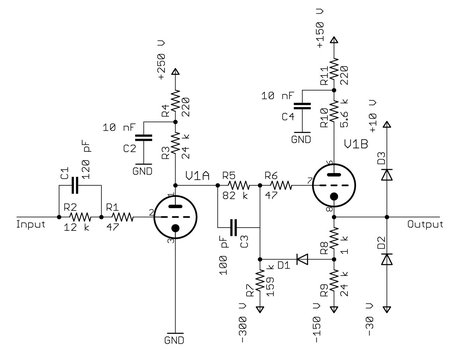
Figure 5.23: Model A DC inverter (see [IBM BASIC CIRCUITS][p. 50])
5.10 Flip-flops
One of the most basic, yet central elements in a digital computer is of course the flip-flop. The AN/FSQ-7 featured three basic flip-flop models310 as shown in table 5.2 which also contains the abstract circuit symbols used to denote these building blocks. Two of these flip-flops are discussed in the following, the model B low-speed311 flip-flop and its model A high-speed counterpart.
The circuit of the low-speed flip-flop is rather simple as it closely resembles that shown in figure 2.6, section 2.2: Two inverting amplifiers, consisting of the tubes V1A and V1B, are connected in a crosswise fashion with the plate of one tube driving the other’s control grid and vice versa. Since the circuit is symmetric in its nature and must exhibit two stable states, the corresponding resistors R7 and R8, R5 and R6, R3 and R12, R2 and R11 must have corresponding values.312
| Logic block symbol | Characteristics | |||
|---|---|---|---|---|
| Model | Pulse input | Level input | Speed | Drive capability |
| A | High-speed | Can drive load directly | ||
| B |  |
Low speed | Cannot drive load directly | |
| C | 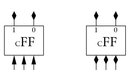 |
Even lower speed | Can drive load directly | |
Table 5.2: Flip-flop types and their respective characteristics (see [IBM BASIC CIRCUITS][p. 51])
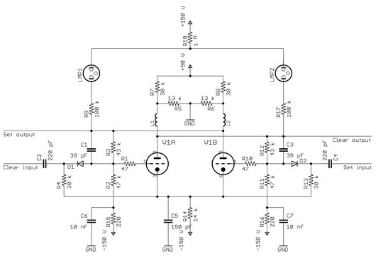
Figure 5.25: Model B low speed flip-flop (see [IBM BASIC CIRCUITS][p. 54])
If the flip-flop is in the set-state, V1A is conducting. Accordingly, the potential at its plate is negative, so that tube V1B is cut off due to the negative potential at its control grid. Thus, the left output is at a positive voltage while the right output is negative. The upper and lower levels for these output lines, +10 V and −30 V respectively, are determined by two voltage dividers for each output. The output voltage for the left output is determined by the voltage divider consisting of R6 and R8 in the plate circuit of V1B and a second divider consisting of the resistors R3 and R2.313 The same holds true for the right signal output, where the voltage dividers are R7, R5 and R12, R11.
A negative transition of the left input will cause a negative pulse at the cathode of D1, due to the differentiation performed by C1 and R1. Only negative pulses can pass diode D1 and will cut off V1A which will in turn change the voltage at its plate to a positive value turning on V2B. Now the right output is at +30 V while the left is at −10 V. To speed up transitions in either direction, resistors R3 and R12 are paralleled by capacitors C1 and C3.314 In addition to that, two coils, L1 and L2, are wired in series to the plates of V1A and V1B, acting as so-called peaking coils.
The input circuits shown here, C2, R3, D1, and C3, 13, D2 are used for level inputs. If this model B flip-flop is to be used with standard pulses as input, each input is connected to the secondary of a pulse-transformer. This secondary winding is shunted by an additional diode against ground so that positive levels won’t reach the differentiating capacitor of the flip-flop. The primary side of each of the two pulse-transformers can be driven by a number of pulse inputs each decoupled by a dedicated diode which is oriented in such a way that only positive pulses can reach the transformer.
The reason that this type B flip-flop cannot drive external loads directly is due to the way the output signals are generated: Since there is no active clamping by diodes, the output voltage will deviate more or less from its nominal values of +10 V and −30 V depending on the load. Thus, this flip-flop can only drive DC inverters or level setters which are then connected to additional circuitry. The difference between this and the model C flip-flop is that the latter uses a slightly different scheme for generating the two output signals including two clamping diodes to ensure a proper output level even under load.
Figure 5.26 shows the detailed schematic of a model A high-speed flip-flop capable of operation at up to 2 MHz pulse repetition rate.315 The main difference to the circuit discussed above is the addition of two cathode follower stages comprised of the tubes V1A and V2A which serve a double purpose: First, they allow driving a load directly at the two output lines. Second, they decouple the control grid of V2B from the plate of V1B and vice versa thus speeding up the overall operation of the flip-flop. Since the cathode follower V1A amplifies the output signal at the plate of V1B, both triodes are contained in the same glass envelope to minimize wire length and thus stray capacitances in the circuit further speeding up its operation. Another difference to the model B flip-flop is the higher plate voltage of +150 V.
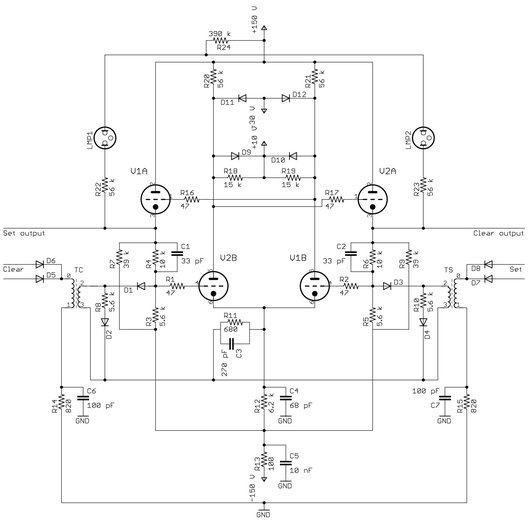
Figure 5.26: Model A high-speed flip-flop (see [IBM BASIC CIRCUITS][p. 58])
5.11 Single-shots
A single-shot316 as has been used in AN/FSQ-7 is triggered by a standard pulse and generates a (non-)standard level output signal with a specified duration t. This output signal can either be at a negative level during the quiescent state of the single-shot and raise to a positive level or vice versa. Three different models, B, C, and D, were used as standard components. Figure 5.28 shows the abstract circuit symbol of such a single-shot. As before, the particular model is denoted by a small capital letter.
Figure 5.27 shows the different behavior of the model B, C, and D single-shots. All three are triggered by a standard pulse shown at the very top of the figure. While model B and C generate a standard level output signal, type D yields an output signal swinging between −42 V and +17 V. Since single-shots exhibit only one stable state they are also known as monostable multivibrators, one-shot multivibrators,317 or gating multivibrators.
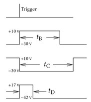
Figure 5.27: Single-shot behavior

Figure 5.28: Symbol of a model B single-shot
Figure 5.29 shows the detailed schematic of a model B single-shot, yielding a positive amplitude with a duration of tB at the standard level output when triggered. The heart of the circuit consists of the tubes V1A and V1B. V2A is just an output stage based on a basic cathode follower. While the single-shot is in its stable (quiescent) state, V1B is conducting since its grid, being at ground potential, is more positive than its cathode. Accordingly, the junction between R8 and R9 is at −30 V due to the clamping diode D5 so that diode D3 conducts. This holds V1A in its cutoff state as its grid is now more negative than its cathode which is clamped to −15 V by means of D2, so the single-shot remains in its current stable state.
An incoming standard pulse trigger is inverted by transformer TI. A negative pulse reaches the plate of V1A through D1 (the coil L1 is a high resistance path for such a pulse while it exhibits low DC-resistance). From there it reaches the grid of V1B through C3 thus lowering the current through this tube, which results in a rise of its plate potential. This causes the negative potential at the grid of V1A to rise accordingly, and V1A starts to conduct.
This, in turn, decreases the plate potential of V1A which increases the effect of the initial negative pulse as it couples through C3 to the grid of V1B. Eventually, V1B will be cut off completely. The high plate potential at this tube is clamped by diode D4 to +10 V and amplified by the cathode follower V2A which yields the output signal which is now positive.
Now that V1B is cut off, the coupling capacitor C3 is discharged through R6, so the time-constant of the RC-network determines the length of the standard level output signal generated by this circuit. As a result, the potential at the grid of V1B rises to the point where the tube starts conducting again. Thus the potential at the junction of R8 and R9 falls to −30 V since it is clamped by diode D5 which causes the output of the cathode follower V2A to go low, too. In addition to this, V1A is cut off again through D3 and R4.
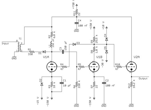
Figure 5.29: Model B single-shot (see [IBM BASIC CIRCUITS][p. 64])
The resistors R4, R5, and R10 suppress parasitic oscillations which could be caused by the inherent grid-capacitances of the tubes. R11, C4 and R7, C2 form basic decoupling networks for the positive and negative supply lines while C1 creates a low reactance path for the cathode of V1A, reducing its switching time.
The input circuit shown in figure 5.29 – consisting of TI, R1 and D1 – is the so-called low-speed input as it is used for output signal-widths 4 µs ≤ tB ≤ 105 µs with 68 pF ≤ C3 ≤ 500 nF and 220 kΩ ≤ R6 ≤ 700 kΩ. In cases where a much shorter output-pulse width 1 µs ≤ tB ≤ 4µs is required, this simple input circuit does not suffice. An active input circuit is necessary then:318 A fourth triode is added which is connected with its plate to the plate of V1A, while its cathode is connected to +10 V. The grid of this tube is connected to the secondary of an input transformer like TI. This transformer does not invert the trigger pulse so that this tube conducts heavily during an input pulse, pulling down the plate of V1A faster than with the simple input circuit shown in figure 5.29.
The model C single-shot is based on model B with an additional inverter for the output signal, while model D features an output stage consisting of two paralleled cathode followers capable of driving high loads.

5.12 Pulse generators
While a single-shot converts a standard pulse into a standard level signal, a pulse generator 319 does more or less the opposite: An incoming pulse or a standard level signal which may be generated by a manually operated button or a cam-controlled switch, is converted into an output pulse. All in all, five different pulse generator models, denoted by letters A through E, were used. The symbols for these devices are shown in figure 5.30.
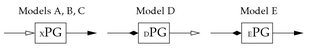
Figure 5.30: Pulse generator symbols
The models A, B, and C feature a non-standard pulse input and are based on a thyratron – their circuit, shown in 5.31, is rather similar to that of a thyratron relay driver: Pressing the switch S1 causes a positive going pulse through C1 which ionizes the thyratron, lowering its plate potential. This, in turn, generates an output pulse on the secondary side of TO. The main difference to the thyratron relay driver is the RC-COMBINATION R7, C2: During the quiescent state, C2 is at +250 V through R8. When the thyratron ionizes, a rather large current flows through V1. This discharges C2 until the potential difference between anode and cathode of the thyratron is below the ionization threshold thus extinguishing the thyratron automatically.
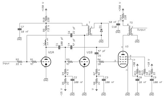
Figure 5.32: Model E pulse generator (see [IBM BASIC CIRCUITS][p. 75])
In some cases, due to a bouncing switch S1 etc., this simple reset circuit is not sufficient since multiple output pulses might be generated through a single activation of S1. In such cases a normally closed (NC for short) switch is connected in series with R8. This switch is then built as part of S1 in such a way that it opens just before S1 closes, so only the energy stored in C2 is available to generate a single output pulse.
The models A and B differ only with respect to R4 which is 200 kΩ for a type B pulse generator. Model C does not feature the switch input circuit consisting of S1, R5, and R4, instead the input pulse is coupled directly to capacitor C1.
The model D and E pulse generators are based on the principle of the so-called blocking oscillator.320 Figure 5.32 shows the detailed circuit diagram of model E which expects a standard level input of +10 V during its quiescent state and generates an output pulse when this level drops to −30 V. Its output stage is straightforward and consists of a pentode driving a pulse transformer TO. The interaction of the two triodes V1A and V1B deserves more attention: With a +10 V input level, V1A is conducting since its grid is well above ground potential, while V1B is cut off since its grid is tied to −15 V by the resistors R3, R4, and R5.
When the input signal changes to −30 V, V1A is cut off and its plate potential rises to +150 V. This signal is differentiated by C1 causing a positive pulse at the grid of V1B which begins to conduct. This causes a current to flow through the primary of transformer T which results in a positive going pulse at its secondary. This triggers the output pentode through C5 and causes the grid of V1B to rise even higher. This increase in grid potential causes a grid current to flow thus charging both coupling capacitors
C1 and C4. Since the transformer T actually performs a differentiation operation, the pulse generated at its secondary will fall back to ground potential causing the right hand side of C4 to be grounded. This adds to the negative grid bias of V1B, effectively blocking the tube. As soon as C1 and C4 have discharged through R4 and R5, the pulse generator is ready for the next falling edge of its input signal.

Figure 5.33: Basic schematic of a discrete-constant delay line (see [IBM BASIC CIRCUITS][p. 77] and [HUGHES 1949][p. 730])
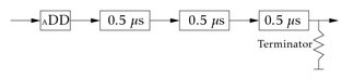
Figure 5.34: Typical delay line setup (see [IBM BASIC CIRCUITS][p. 78])
5.13 Delay lines and delay line drivers
So-called delay lines had been in use since World War II to delay complex signals like those delivered from radar devices for several µs.321 Basically, a delay line consists of a series of LC-filters, combinations of coils and capacitors as shown in figure 5.33.322 An arrangement which is called a discrete-constant line.323
An incoming pulse charges C1, thus raising the potential across C1. As a result, a current starts to flow through L1 which in turn charges C2 and so on. The resistor R1 terminates the output of this discrete-constant delay line so that a pulse will not be reflected back to the input again. A typical so-called delay unit exhibits a delay of 500 ns while the taps T1, T2, and T3 allow shorter delays, too. Figure 5.34 shows a typical delay unit arrangement where three 500 ns delay units are connected in series giving an overall delay of 1.5 µs.
While single delay units can be driven by a standard pulse amplifier as shown in section 5.3, chains of delay lines require a special driver circuit, the so-called delay line driver. Figure 5.35 shows the schematic of such a driver: The control grid of the pentode V1 is negatively biased at −30 V through R3, the secondary of TI, and the parasitic suppressor R1, making sure that V1 is cut off initially. An incoming pulse at the primary of TI will cause a positive pulse on its secondary which in turn causes V1 to conduct. The current flowing through R6, the primary side of TO, and V1 causes the generation of a high-power output pulse on the secondary of TO which is connected to the input of the delay unit chain to be driven. Since the suppressor grid of V1 is connected to the anode, the pentode is actually operating as a tetrode allowing a higher current to flow through V1.
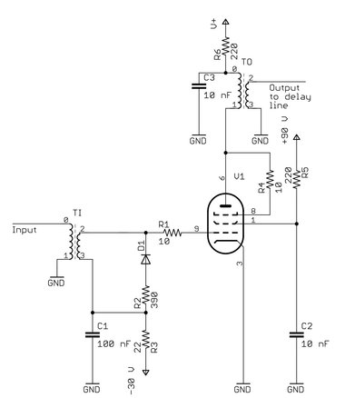
Figure 5.35: Delay line driver circuit (see [IBM BASIC CIRCUITS][p. 78])
5.14 Special circuits
Although the basic circuits described above were the main building blocks of an AN/FSQ-7 installation, there was a plethora of so-called special circuits324 necessary for various purposes: Core memory row-, column-, and inhibit-drivers, sense amplifiers amplifying the tiny currents induced in the sense wires, core shift circuits to convert parallel data into serial data-streams suitable for data transmission over telephone lines, pulse shapers for amplifying the amplitude and reducing the width of pulses, binary decoders325 to generate the deflection voltages for the various displays, deflection amplifiers, drivers, and vector generators for displays, amplifiers for area discriminators and light guns, crystal oscillators, data transmission and receiving circuits, drum reading and writing amplifiers, SCHMITT trigger circuits, tuning fork oscillators to generate stable low-frequency signals, and even sine-cosine approximators used in the input equipment for processing azimuth data.326
Neither these circuits nor the intricate regulated power supplies, voltage failure detectors, missing-pulse detectors, etc. will be described in detail in the following. Some additional information will be given in sections where units incorporating such devices are covered.
5.15 Pluggable units
Combinations of the basic devices described in the previous sections were mostly packaged in standard plug-in modules, called pluggable units as shown in figure 5.36. There were two basic variants of this basic packaging unit: One capable of holding up to nine vacuum tubes and one designed for six tubes. The mounting of the tubes is particularly noteworthy: The front plate of such a module has holes for the tubes which exhibit a larger diameter than the tubes themselves. Thus cold air supplied from the air conditioning equipment entering the computer’s frames will escape through these gaps forming a cooling sheath of air around the tubes. The necessary passive components like resistors, capacitors, diodes, and coils were mounted behind the tubes on both sides of phenolic base cards – forerunners of today’s printed circuits boards.327 These cards were populated with the passive components and then dip-soldered during the manufacturing process. Compared with other digital computer modules from the same time frame, these modules look rather bulky and do not exhibit a density as high as similar modules of commercial computers like the IBM 701. The reason for this was maintainability: Tubes could be changed without the necessity of removing such a pluggable unit. More complex faults could be solved in a matter of minutes at most, by swapping a defective unit with a known good one. The low mean time to repair was very well worth the price of a larger footprint of the overall machine.
Figure 5.37 shows a module being repaired. Each AN/FSQ-7/8 installation featured repair workbenches like that shown in figure 5.38 which contained the necessary power supplies for operating single modules, as well as measurement equipment including a Vacuum Tube Voltmeter (VTVM) and an oscilloscope. External connections could be made on a patch field which contained a jack for every connection of the module as well as some signal sources like standard pulses and levels etc.

Figure 5.36: Typical nine-tube plug-in module (see [IBM BASIC CIRCUITS][p. 7])

Figure 5.37: Plug-in module undergoing service (see [Armed Services Press 1979][p. 10])

Figure 5.38: Front view of the module tester (courtesy of Mr. RON BRUNELL)
Figure 5.39: FETRON as a replacement for a 6AK5 pentode (see [Teledyne 1972] and [BURMAN 1972])

Figure 5.40: Production steps of a FETRON (see [Teledyne 1973][p. 4])
5.16 The FETRON
An interesting, yet short-lived development began in May 1977 at McChord AFB: A $ 100,000 testing program was set up to determine if the life-time of its AN/FSQ-7, affectionately called “CLYDE” by its staff, could be extended while reducing the overall operational costs by replacing a substantial part of its vacuum tubes, mainly pentodes, with a solid state device known as “FETRON”.328
Development of the FETRON started in early 1970 at Teledyne Semiconductor with the aim of creating a pin-compatible semiconductor-replacement for vacuum tubes which were still used abundantly in various equipment and caused increasing maintenance efforts in those years.329
The FETRON is based on the junction field-effect transistor – the simplest field-effect transistor of all which already exhibits a vacuum-tube-like behavior. Figure 5.39 shows the simplified schematic of a FETRON suitable as a replacement for 6AK5 pentodes: At its heart is a cascode configuration of two JFETs, the lower left one determines the input characteristics of the device while the upper right JFET increases the ability to withstand the high voltages found in typical vacuum tube circuits. Not shown in the schematic is a tantalum fuse in the plate line to protect the surrounding circuitry in case of a failure.330 Figure 5.40 shows the various production steps of a FETRON: The JFETs are mounted on a thick film substrate forming a hybrid circuit which also holds the tantalum fuse and optional RC-networks to tailor the device’s performance to that of a specific vacuum tube to be replaced. The connectors of the FETRON protrude through its bottom plate and allow a one-to-one replacement of vacuum tubes under ideal circumstances.331
CLYDE’s circuitry proved to be more challenging than other areas of application where FETRONs fitted in rather easily. About 9,000 diodes had to be replaced by more modern types to allow the replacement of more than 40,000 vacuum tubes. It was estimated that the break-even point regarding the expenses for this massive retrofit including the vast amount of manual labor would be reached after only 19 months of operation due to savings in power, air conditioning and lower maintenance efforts.332
As successful as this conversion of CLYDE proved to be – eventually, about 70% of CLYDE’s tubes were replaced by FETRONs under a $ 400,000 contract333 – it had no substantial effect on the life-time of the remaining installed AN/FSQ-7 base – the last machines were shut down for good in 1983.
5.17 Troubleshooting
Troubleshooting a machine as complex as a duplex AN/FSQ-7 central computer is by no means an easy task and would have been impossible without the aid of marginal checking and intricate diagnostic software routines. MIKE LOEWEN, a former computer maintenance technician remembers:
“The final part of [the] training program involved pulling a random tube from the standby system, and having me deduce its location using the Duplex Maintenance Console (DMC) and available diagnostics procedures.”334
In some cases, troubleshooting could become a nightmare, especially when the problem was intermittent, as DAVID E. CASTEEL remembers:
“In a more serious vein, we had a problem with the B computer for several months. Although it always passed its maintenance checks, when it was active and processing the Air Defense picture, every so often very strange things would suddenly happen: Sometimes the displays would just fly to the edges of the Situation Display; sometimes features that had been selected to operate would just drop out of operation; or the converse – features that had not been selected would suddenly begin functioning. For a couple of months no one could find what was causing these strange things to happen. Eventually, [it turned out] that at least some of problems were associated with a pick or drop of one particular bit [. . . ] – the features starting or stopping were all associated with that bit in a [control] word [. . . ] We organized a plan to remove and replace every one of the pluggable units in the B computer associated with movement or changing that particular bit (dozens of them) and each was marked with where it had been mounted. Then over time we put each of those units back into its original position and left the machine to run. Eventually, we reached a point where the problems returned and thereby could identify the defective unit. Close examination revealed that there was a resistor with a hairline crack in it that sometimes was in contact and other times was not, producing spikes in the signal passing through it. That resistor was replaced and the problems stayed fixed.”335
Despite the unique challenges of maintaining these intricate computers, the reliability achieved was (and still is – even from today’s perspective) extremely remarkable: [BELL 1983][p. 14] quotes an uptime of 99.83% for a simplex machine and 99.97% for duplexed operation. Detailed performance and availability figures were collected for the last seven AN/FSQ-7 installations from March 1978 to February 1980:
“The average percentage of time that both machines of a [duplex] system were down for maintenance was 0.043 percent, or 3.77 hours per year. The average percentage of time both machines were down for all causes, including air conditioning and other situations not attributable to the computers, was 0.272 percent, or 24 hours per year.”336