
6 Central processor
The AN/FSQ-7 central processor consists of a number of interconnected elements as shown in figure 6.1. Basically, it is a classic VON NEUMANN-architecture with a central memory subsystem holding instructions as well as data. Depending on perspective, the AN/FSQ-7 can be seen with some justification as a 16 bit computer or a 32 bit computer: The memory word-length is 32 bits plus a single parity bit for error checking purposes, while the basic operations of the computer itself work on 16 bit values in one’s complement. It has been designed this way because the air defense application required a high amount of coordinate transformations. Accordingly, it was decided to implement an arithmetic unit337 capable of working on two 16 bit values at a time. So while single data words are restricted to 16 bit in length, the AE, consisting of a left and a right AE, processed two such quantities at a time thus requiring a 32 bit memory data path. Correspondingly, a memory word is divided into a left half-word and a right half-word of 16 bits each.338 Such a half-word x has the same structure as the machine word of Whirlwind as shown in figure 3.1, section 3.1. It is interpreted as a value -1 + 2-15 ≤ x ≤ 1 - 2-15.
The basic timing unit is the 6 µs memory cycle denoting the time necessary to read or write a word from or to memory.339 One to three such memory cycles make up a so-called instruction cycle, the time necessary to execute a single instruction. In this case these cycles are called machine cycles to distinguish them from the timing units required for pure memory accesses. While some instructions, like transferring a value from one internal register to another, can be completed in a single memory cycle, other instructions require up to three cycles to fetch or write operands etc. These are denoted as Program Time (PT), Operate Time A (OTA), and Operate Time B (OTB) respectively, see figure 6.2.
A machine cycle is subdivided into twelve timing pulses, TP 0 to TP 11,340 which control the generation of either instruction pulses controlling the execution of an instruction (PT, OTA, OTB), or breakout or break-in pulses which control the transfer of data from memory to an output unit or from an input unit to memory.341 Quite similar to the control of Whirlwind,342 the actual execution of an instruction does not start with TP 0 but with TP 7. TP 0 to TP 6 belong to the preceding instruction, allowing an overlapped instruction fetch from memory. Accordingly, a single memory cycle operation will start at TP 7 and will end at TP 6 of the next machine cycle. Since the following instruction has already been fetched during TP 0 to TP 6 of this cycle, its execution starts with the next pulse TP 7.
Figure 6.1: Basic circuit groups of the AN/FSQ-7 (see [IBM CCS I][pp. 235 f.])


Figure 6.2: Memory/instruction cycles and cycle types
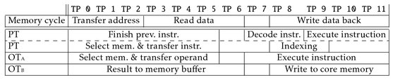
Figure 6.3: Typical sequence of machine cycles during instruction execution (see [IBM CCS I][p. 90] and [IBM CCS XD][p. 29])
Figure 6.3 shows a typical sequence of timing pulses controlling the execution of an instruction. The first eight pulses used for the instruction fetch look like this:
TP 0: This is actually PT 0 and causes the memory address register343 to be cleared in preparation of the following transfer of a new memory address.
TP 1: The memory buffer registers are cleared and the contents of the program counter are transferred to the memory address register initiating a read access which takes four pulse times to complete.
TP 6: The operand-address and operation registers344 are cleared.
TP 7: The instruction read from memory is transferred to the operand-address (right half-word of the memory buffer) and operation registers (left half-word);345 the program counter is incremented to prepare for the next instruction fetch. Since readout is a destructive operation in core memory systems, the remaining cycles TP 7, . . . , TP 11 are used by the memory subsystem to write the word just read back to the core stack.
Some instructions, like multiplication, division, and shifting required more time than the 18µs of three consecutive memory cycles. These were implemented by suppressing the generation of timing pulses for a predefined duration. During this arithmetic pause all other central computer activities were paused. A multiplication took 32 timing pulses to complete, corresponding to 16 µs while a division instruction required 104 pulses (52 µs).

Figure 6.4: Detailed, partial view of the second floor of a SAGE building, housing the central computer system (see [IBM AN/FSQ-7][p. 36])
The following sections will now focus on the various subsystems of the central computer system as shown in figure 6.1: The memory element, the instruction control element, the program element, the arithmetic element, the selection element, the input /output element, and finally, the various manual control facilities necessary to control the duplexed computer system, the power supply and marginal checking system. Figure 6.4 shows the arrangement of the central subsystems of the computer itself on the computer room’s floor.
6.1 Memory element
The so-called memory element was based on the core memory system developed for Whirlwind. Figure 6.5 shows a typical core plane as used in the early core memory systems for AN/FSQ-7. This plane contains 26 × 26 = 4096 individual cores. 36 such planes were stacked above each other, but only 33 of these were used for a 32 bit memory word and parity – the remaining three planes were used as spares and could be used to replace failed planes by rewiring the memory stack without the necessity of dismantling and rebuilding the stack as a whole.

Figure 6.5: A single 64-by-64 core plane (see [IBM MEMORY ANALYSIS][p. 5])
Figures 6.6 and 6.7 show a complete memory element from its back (wiring) and front (plug-in) side. The shower stall containing the central core stack as well as the necessary 64 row and 64 column line drivers – clearly visible as groups of 16 tubes above and below the stack on all sides – can be seen in figure 6.6.
One driver out of each of these two groups of 64 driver circuits was selected by the two six bit halves of a twelve bit address by means of a diode decoder circuit similar to that shown in figure 3.12 in section 3.1.2.346 In addition to these drivers, 33 so-called digit plane drivers are necessary to control the inhibit wires of the 33 planes of the core stack. In addition to this, the 33 sense wires require 33 differential amplifiers.
XD-1 and XD-2 were originally equipped with two such memory elements for a total of 8192 words of 32 bits plus parity of memory. It soon became clear that this was not sufficient for the solution of the air defense problem as HERBERT D. BENINGTON remembers:
“[W]hen we had the XD-1 (the prototype of the AN/FSQ-7 computer) operating and had 8000 words of core[, ] I started realizing then that we couldn’t get the job done because there would have to be so much paging in and out from drums that we’d spend too much of our available time doing that. I was also having lunch with my boss that day, and I told him my conclusions. JAY [W. FORRESTER] dropped by at lunch and said, ‘Well we’ve been developing a 65,000-word core memory, so we’ll put it in.’ That eightfold increase made the program possible.”347

Figure 6.6: 4 k Core memory system, wiring side (see [IBM MEMORY ANALYSIS][p. 4])
Accordingly, one of the 4 k memory elements was replaced by a 64 k memory element, 348 a massive and complex retrofit which affected nearly every part of the overall computer system due to the longer addresses required.349 Figure 6.8 shows the core stack enclosure of such a 64 k memory system. With one 64 k and one 4 k memory a 17 bit address was necessary while the system was originally designed for a 16 bit address. Thus, all parts of the computer involved with address handling had to be modified. As a part of this change the AE was modified adding a special mode in which both 16 bit halves of the arithmetic element could work together on a 17 bit value instead of working in parallel on different data at a time.

Figure 6.7: 4 k Core memory system, plug-in side (see [IBM MEMORY ANALYSIS][p. 3])
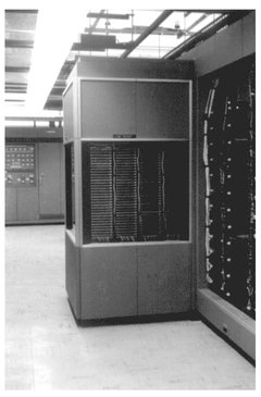
Figure 6.8: 64 k core memory array (courtesy of Mr. PETE KARCULIAS)
Eventually, two systems, the XD-1 which was used by System Development Corporation (SDC) for software development, and the AN/FSQ-7 installation at Luke AFB, were even further extended by replacing the remaining 4 k memory element by a second 64 k element. This was necessary as Luke AFB became the primary programming site and thus required more memory than the other DCs.
In addition to this core memory element, AN/FSQ-7 featured a so-called test memory . It contained 16 read-only memory locations of 32 bits each which could be programmed manually using a patch panel similar to those used in contemporary punch card equipment. In addition to this, the test memory embraced two manual toggle switch registers, each consisting of 16 switches mounted on the maintenance console, and one 16 bit flip-flop register. The latter register was the only memory location in test memory which could be written under program control. Of these 19 memory locations, only 16 could be addressed at one time. Using four control hubs on the patch panel, basically every combination of these 16 read-only memory cells, the two toggle registers and the flip-flop register could be mapped to this 4 bit address space comprising the test memory.350 The test memory was typically used during maintenance operations to store small test programs. These programs would normally test the core memory system and after this had been found fully operational, larger and more intricate test programs could be run from core memory, testing the overall computer system.
6.2 Instruction control element
The instruction control element351 resembles what would be called a microprogrammed control unit today. It has been aptly described as being “the internal control center of the computer since it contains the master-timing and control circuits which are necessary to sequence, co-ordinate, and control all internal operations required to execute the stored program.”352

Figure 6.9: Principle of operation of the instruction control element (see [IBM CCS XD][p. 63])
As shown in figure 6.9, it is controlled by the bit pattern representing an instruction as read from core memory. The heart of the instruction control element is the so-called DC level generator which consists of a number of diode matrices receiving individual parts of an instruction.
Each AN/FSQ-7 instruction is specified by a class code denoting the class (like add, shift, etc.) the instruction belongs to, a variation code specifying the particular variant of the instruction, and several index bits controlling which – if any – of the available index registers is to be used for address calculations. Accordingly, the instruction control element contains three decoder matrices.353 These matrices, in turn, generate a variety of DC level output signals controlling gate tube circuits.354 These gates also receive fixed timing pulses at their respective pulse inputs. The output pulses of these circuits are then used to control the various components of the computer system. Accordingly, these gate tube circuits are called command generators.
Figure 6.10 shows one of these decoding matrices, the variation matrix, in detail: Four bits of the operation register are decoded by means of a number of diode AND gates connected to the normal and inverted outputs of the register’s flip-flops. All in all, the instruction control element is capable of issuing 162 different so-called commands in order to execute the 59 different AN/FSQ-7 instructions.355
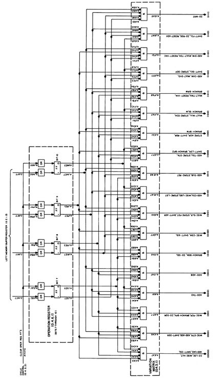
Figure 6.10: Implementation of the variation matrix of the instruction control element (see [IBM CCS XD][p.75])
Having a look at the detailed floorplan of an AN/FSQ-7 installation shown in figure 4.10 reveals that the instruction control element, unit 4, occupied a frame holding eight logic bays, each capable of holding up to 20 plug-in modules and one power distribution section. This frame contained 40 nine-tube modules of the type shown in figure 5.36, and 117 six-tube plug-in modules.
6.3 Selection and IO control element
The selection element356 extends the instruction control element as it takes care of six special machine instructions which differ from the remaining instructions in that they control or sense external circuitry. These instructions are the following:
BSN: Branch on sense – depending on the current state of a so-called sense unit a conditional branch can be executed, altering the program flow.357
PER: Short for operate, this instruction controls operate units like condition lights, intercommunication equipment, interlock logic, magnetic tapes, line printers, card punches and readers, marginal checking equipment, etc.358
TOB and TTB: The test one bit and test two bits instructions compare one bit or two consecutive bits in a 32 bit word stored in core memory with a specified pattern and conditionally skip the following instruction.359
SEL and SDR: The select and select drum instructions select input/output devices and drums for subsequent data transfers to and from the central computer.360
Figure 6.11 shows the simplified block diagram of the selection element: It is controlled by the six so-called index interval bits of the instruction currently being executed and generates the necessary control signals for selected devices etc. The PER SEL BSN-matrix is a diode decoder matrix similar to those used in the instruction control element.
The IO control element is part of the input/output subsystem of AN/FSQ-7 and provides the actual interface to input/output devices under control of the select instructions (SEL and SDR) and the instructions to load the input/output address counter (LDC, load IO address counter), and to read (RDS) or write (WRT) data from and to input/output devices. In contrast to most of its contemporary computer systems and even many of today’s computers, AN/FSQ-7 did not support direct input/output in which data is transferred synchronously under program control between the computer system and some input/output device.

Figure 6.11: Block diagram of the selection element (see [IBM CCS I][p. 177])
Instead, such outbound transfers were implemented as break-in (from an external device to the central memory) or breakout transfers. To initiate such a transfer, address information must be supplied and an input/output element must be selected. Following this a break cycle will be initiated, causing the central computer to suspend operation for a 6 µs cycle, during which an automatic transfer of one data word takes place.361 Accordingly, the IO control element would be called a direct memory access362 controller today. It should be noted that AN/FSQ-7 did not support any interrupt processing at all, so it was not possible to interrupt a running program by an external event to perform some interrupt service routine. These break-cycles only halted a program for a single memory cycle after which program execution continued seamlessly.
6.4 Program element
While other digital computers of the 1950s had only one central control unit taking care of instruction decoding and execution, as well as of controlling the overall program flow, these tasks were handled by two different units in AN/FSQ-7. In addition to the instruction control element it featured a so-called program element363 being responsible for selecting memory addresses for reading instructions and data, keeping track of the overall program flow, coordinating input/output operations and indexed addressing. Therefore the program element not only contains the program counter but also address counters for input/output operations, input/output buffer registers, and index and address registers as shown in figure 6.12.
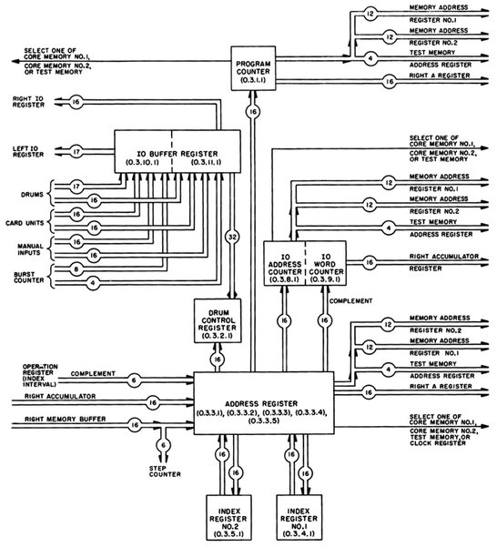
Figure 6.12: Block diagram of the program element (see [IBM CCS XD][p. 211])
The address register receives data from a variety of sources like the address part of an instruction word, from index registers, or the right accumulator. Its main purpose is to supply address information to the memory system and the program counter in case of branches. It also furnishes address information for accessing the magnetic drums. The IO address counter and the IO word counter shown in figure 6.12 are used for break-in and breakout transfers resembling today’s DMA transfers. Not shown is the index adder which is used for computing a memory address from the contents of the right accumulator and one of the available index registers.

Figure 6.13: Implementation of the program counter (see [IBM CCS XD][p. 220])
The original implementation of the program counter of XD-1 and XD-2 is shown in figure 6.13. Since these machines had two 4 k core memory systems, a 13 bit program counter was sufficient and, accordingly, only bits 3 to 15 had been implemented. The individual address bits are implemented as flip-flops, each feeding the conditioning input of a gate tube circuit. Since these gate tubes are conditioned by the 1-output of the flip-flops, they effectively propagate any carry signals generated during one increment operation.
Figure 6.14 gives an overall impression of the instruction decoding process showing the interplay of all elements discussed so far.
6.5 Arithmetic element
The arithmetic element364 was the heart of the AN/FSQ-7 computer – it implements all of the basic data manipulations operations like add, subtract, multiply, divide, shift, and many more. AN/FSQ-7 had to perform a lot of coordinate transformations from polar coordinates as delivered from the radar stations to Cartesian coordinates as required by the display subsystems. In contrast to most scientific digital computers of the 1950s, featuring long machine words of 36 or 40 bits, a short word length of 16 bit was sufficient for this type of processing given the limited precision of incoming radar data. To speed up the data processing, two such 16 bit words were stored in one 32 bit memory cell. Accordingly, the arithmetic element was implemented as two 16 bit arithmetic units working in parallel on both halves of a 32 bit word.
Figure 6.15 shows the block diagram of the arithmetic unit: Each half is quite similar in structure to the arithmetic element of Whirlwind and consists of an A-register (AR), a B-register (BR), and an accumulator (AC) for storing data. The central data processing element is the adder which is connected to the AC and the AR. Both halves can exchange data by shifting single bits from the left accumulator to the right or vice versa. The left and right memory registers shown at the very top of figure 6.15 are actually part of the arithmetic element to reduce the overall wire count and to keep wire lengths down at a minimum. In addition to these registers, the arithmetic element contains left and right IO registers, test registers, and a clock register.365

Figure 6.14: Instruction decoding in AN/FSQ-7 (see [IBM PGM][p. 44])
The implementation of a single bit full-adder366 is shown in figure 6.16. The left and right adders each contain 16 of these building blocks as well as a lot of other equipment to implement other instructions like shift, multiplication and division. The two flip-flops at the left hand side of figure 6.16 hold two corresponding bits of the AC and the AR of one side of the arithmetic element. Their inverted and non-inverted outputs drive four AND gates corresponding to the four possible bit combinations during an add operation. Since 1+0=0+1, two of the AND gates feed an OR gate, so that this first stage of the adder generates three mutually exclusive output signals.

Figure 6.15: Block diagram of the arithmetic element, left and right half (see [IBM CCS I][p. 114])
Six gate tube circuits then combine these three output signals with the non-inverted and inverted carry signal from the preceding stage, yielding six output signals which are then combined to generate the sum and carry outputs. A short example may clarify the this circuit’s operation: Assume that the upper flip-flop is set to 1 while the lower one is 0. Assume further that the preceding stage has generated a carry: Since this combination of AC- and AR-bits activates the second AND gate, the OR gate will yield the value 1 at its output. Accordingly, the two center gate tube circuits are in the conditioned state. Since a carry signal is present from the preceding stage, the right gate tube driven by the OR gate generates an output pulse. This causes a pulse only on the inverted sum output line denoting the sum 0. In addition to this, a pulse is also generated on the non-inverted carry output line, denoting a set carry bit for the following adder stage.367
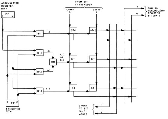
Figure 6.16: Single bit adder stage of the arithmetic element (see [IBM CCS XD][p. 144])
To get an impression of the complexity of the left and right arithmetic element, figure 6.17 shows the block diagram of the circuitry necessary to implement the instructions ADD, SUB, TAD (twin add), and TSU (twin subtract).368 Similar to Whirlwind, the B-register is used for shift operations – its sign bit portion is shown on the far right, connected with the accumulator and the adder stages. As can be seen, the AC, AR, and the adder form a single functional unit with the A-register holding one source operand for an operation and the accumulator holding the other operand. The result of the operation will then be stored in the accumulator.
A more careful inspection of figure 6.17 reveals an interesting feature: The result of an add operation is written back to the accumulator, shifted one bit to the right! This highly unusual feature was implemented to speed up multiplication which relies on such right shifts during each single multiplication step. Yet, an add or subtract operation with this feature would yield an erroneous result being wrong by a factor of 2. Therefore ADD, SUB, and their variations required a corrective left shift to counteract this implicit right shift. Since this additional shift fit quite well into the timing scheme of the basic operations, no additional memory cycle was necessary so that this corrective operation did not slow down these basic operations.
Figure 6.17: Implementation of ADD, SUB, TAD and TSU (see [IBM CCS XD][p. 163])
Unfortunately the same does not hold true for division which needs a left shift instead of the right shift so advantageous for multiplications. While the iterative multiplication process can save one shift per iteration, division has to perform two left shifts significantly slowing down this particular instruction.369 DAVID E. CASTEEL, Captain, USAF (ret), remembers:370
“One may think that this technique would be counterproductive, but a major part of the CPU’s time was devoted to making polar-to-rectangular coordinate conversions of the incoming radar data, and each such point conversion required 2 multiplications.371 With each of up to 16 radars reporting as many as 500 data points each antenna scan (nominal 12 seconds at 5 rpm), that is a need to perform 80,000 multiplications each minute, and the designers were looking to save time any way they could. Division on the other hand, was typically used to provide the speed value of a track, and would occur much less frequently.”
The complexity of the arithmetic unit is best demonstrated in figure 6.18 which shows the front and back view of the left arithmetic element: 13 bays, each holding about 20 plug-in modules, were necessary to implement the circuitry shown on the left half of figure 6.15. The leftmost bay on the front view is typical for all frames used in an AN/FSQ-7/8 and contains literally hundreds of circuit breakers. These were used to remove power from a particular plug-in module to allow replacement without having to power down the rest of the frame or even the computer. The telephone visible on the side of the frame is part of the intercom system which allowed technicians working in different areas of the large (and noisy) computer room to communicate with each other.
Figure 6.18: Back and front view of the left arithmetic element (see [IBM CCS I][p. 9])