
3
Embedded Wafer‐Level Ball Grid Array (eWLB) Packaging Technology Platform
Thorsten Meyer1 and Steffen Kroehnert2
1 Infineon Technologies AG, Germany
2 Amkor Technology Holding B.V., Netherlands
3.1 Technology Description
Wafer‐level packaging (WLP) is one of the fastest‐growing packaging technologies on the market today. The performance and dimension shrink requirements of today’s advanced products fit WLP technology better than other packaging platforms for many applications and markets. WLP is packaging on the wafer as received from the wafer fabrication (FAB) facility. In comparison with other packaging technologies, the wafer is not separated into individual die before packaging. Solder balls are attached to the active side of the wafer after under‐bump metallization (UBM) is applied. For WLP, two options are known as shown in Figure 3.1, WLP with and without copper redistribution layers (RDL).
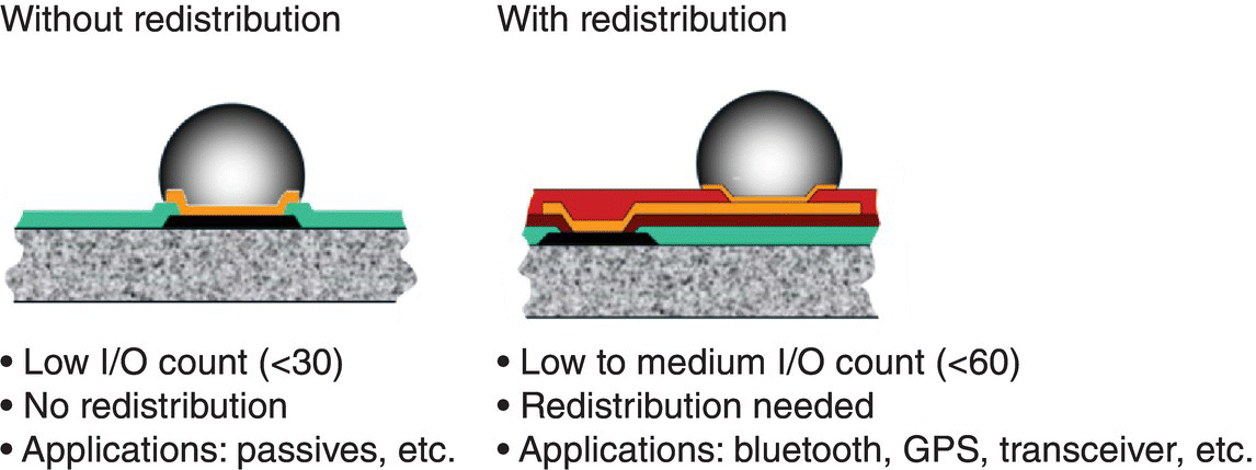
Figure 3.1 Principle of WLP with and without redistribution layer (RDL).
No redistribution is required if the die pads are located at the desired positions of the BGA balls and the die size is smaller than 3 mm × 3 mm – only a UBM and a solder ball are applied. For die with peripheral pad‐out, like typical for wire‐bondable designs, RDL is required. RDL is typically applied with thin film technology, well known from the front‐end processing. A passivation layer (dielectric layer) is normally applied by spin coating, one or more RDL are manufactured by sputtering and electroplating (semi‐additive process), and a final passivation layer again by spin coating.
Finally a UBM may be applied before attachment of the solder ball. Front‐end‐based process steps such as spin coating, lithography, sputtering, and electrolytic plating are the major contributors to this packaging technology. Figure 3.2 shows a sketch of a typical WLP with two RDL (RDL1 and RDL2).

Figure 3.2 RDL stack with UBM for WLP.
A major restriction of WLP is the real estate available for solder balls on the die. All solder balls must fit on the die area. For large pitches or small die, the available space may not be sufficient to position all balls on the die surface, so the use of WLP would not be possible. In order to overcome this ball count and pitch dilemma for WLP, a fan‐out WLP (FO‐WLP) began development in 2005. The version of FO‐WLP technology reviewed in this chapter is called eWLB for embedded wafer‐level ball grid array.
FO‐WLP is the extension of WLP and provides higher input and output (I/O) capability. An area around the die is created prior to the application of the RDL and serves as a fan‐out area for these additional I/O, which typically would not fit on a WLP. All performance and dimension advantages of WLP are enriched by the fan‐out region due to the addition of I/O and, as later discussed, system integration capability. Figure 3.3 indicates the driving factors for FO‐WLP.
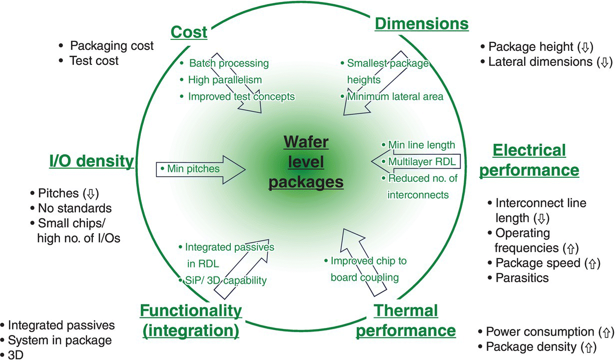
Figure 3.3 Driving factors for FO‐WLP development.
FO‐WLP has been developed primarily for the mobile application market. Infineon was the first company to introduce an FO‐WLP technology called eWLB to the market in 2009. Today, eWLB is in high volume manufacturing at multiple contract assembly suppliers, and many other FO‐WLP variants are offered by other suppliers including foundries and integrated device manufacturers (IDM) in addition to assembly suppliers and are reviewed in this book. Many of them, including those invented by consortiums and universities and also included in this book, are still in the development phase, but some of them recently also started high volume production. The most prominent technology is the integrated fan‐out (InFO) package from silicon foundry TSMC. It was introduced in 2015 and is a high volume product in the mobile arena now.
FO‐WLP can be classified as chip‐first and chip‐last technologies as well as chip face‐up or chip face‐down assembly approach during the wafer reconstitution process. Chip‐first starts with the placement of the die on a temporary mold carrier laminated with an adhesive tape. Afterward, the die on the mold carrier with adhesive tape is embedded with mold compound using a wafer molding process, and after carrier removal, the RDL and solder balls are applied.
In the chip‐last FO‐WLP technology, a thin, typically high density RDL is deposited on a temporary carrier first, and then the die are attached to this layer using typical flip‐chip attach and solder reflow technology. Finally, the mold compound is applied for encapsulation of the die. Chip‐last FO‐WLP is in development and not currently offered in high volume manufacturing. All technologies in production at the time of publication are chip‐first. This is because the first and most prominent member of the FO‐WLP technologies (eWLB) was first to market 10 years ago. The ability to create the thin film and fine line and space dimensions of chip‐last fan‐out has only been developed in recent years.
Chip‐first technology can be distinguished in two different categories: die face‐down or die face‐up assembly approach during the construction of the molded wafer, also called the reconstituted wafer. In the face‐down variant, the die is placed with the active side down on the adhesive tape on the temporary mold carrier. This way, the active side is protected and the mold compound embeds five sides of the die. After removal from the carrier, the reconstituted wafer is coated with the dielectric layer, and the RDL connects to the die pads directly. With this approach, all dies, and potentially other components, placed on the reconstituted wafer have the active side with the die pads on the same plane. Also, multiple die of different thicknesses can be easily embedded in mold compound in the face‐down assembly method.
In face‐up assembly, the active side is placed faceup on the carrier and molded, embedding the active side in mold compound. In order to do this, application of copper pillars is required at the wafer level prior to wafer singulation. For example, copper pillars are typically electroplated copper cylinders on the wafer surface with a height of 20–60 μm and a diameter of 60 μm. After Cu pillar application and wafer saw, the die are placed faceup on the adhesive tape on the mold carrier. This way, the mold compound embeds all five sides of the die. In comparison with chip‐first face‐down FO‐WLP, the active side of the die is now embedded and the die backside is not. A molded wafer grinding step is required to expose the copper pillar and make it accessible for contact by RDL. Both variants are in high volume production: eWLB for chip‐first face‐down FO‐WLP and InFO for chip‐first face‐up FO‐WLP. There are multiple FO‐WLP products on the market. The first product being introduced was a baseband die (see Figure 3.4).
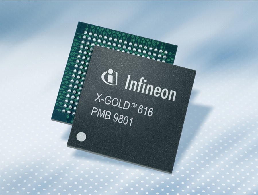
Figure 3.4 X‐GOLD 616 baseband product in eWLB package technology.
The baseband X‐GOLD 61x‐series were monolithically integrated, low power 65 nm baseband devices that included all the digital, analog, and power management functions. Following products in the market packaged in FO‐WLP – face‐down and face‐up assembly approaches – have been RF, audio codec, power management, filters and switches, and combinations in FO‐WLP‐based wafer‐level system in package (WL‐SiP) up to application processors (AP) for the mobile communication market. FO‐WLP started to enter other markets such as automotive, medical and health care, bio‐devices, Internet of things (IoT), and security. Also, microelectromechanical systems (MEMS) have been packaged using FO‐WLP technologies.
3.2 Basic Package Construction
Wafer‐level packages are produced at wafer level, meaning in wafer form, utilizing wafer FAB equipment typically used in front‐end process technology and now also in the back‐end ones. The term front end is used to describe the area and process of processing wafers, e.g. the formation of transistors directly in the silicon. The term back end is used for area and process blocks from wafer separation through packaging until component test. The main innovation in the step from classical WLP to FO‐WLP was the introduction of an artificial molded wafer to generate the fan‐out area. This process is called reconstitution.
Figure 3.5 shows the basic construction of an FO‐WLP. The die is embedded in the mold compound on five sides. RDL, embedded in isolating dielectric layers, redirect the die pads to the interconnect positions for the solder ball. These balls can be placed in the fan‐in zone on the die or in the fan‐out zone on the mold compound.
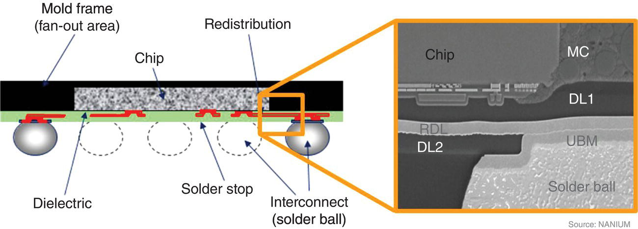
Figure 3.5 Basic construction of FO‐WLP.
FO‐WLP can be used to meet many packaging challenges of today. The reconstituted wafer diameter is independent from the size of the incoming wafer. The reconstituted wafer allows for heterogeneous integration of silicon, GaAs, or SiGe die as well as glass parts, discrete passives, or other packaged parts, like prefabricated vias or prefabricated routing layers. The fan‐out area is adaptable to the area needs, defined by the assembly distance between the die in the reconstitution process.
The challenge of z‐height reduction in mobile applications can be addressed. Package thicknesses below 0.3 mm are possible, because a laminate substrate is not needed for rerouting the signals and the reconstituted wafer can be ground after application of the RDL. The redistribution with shortest interconnects provides best electrical performance and highest interconnect density capability, compared with classical packages. Finally, FO‐WLP is best suited for integration purposes, multi‐die packages, passive integration (in the RDL or as discrete components), and also stacking approaches. In general, the advantages of FO‐WLP are listed below [1].
3.2.1 Cost Performance
FO‐WLP achieves an excellent packaging cost position, especially for small packages. Since it is a fairly new packaging technology on the market, additional opportunities for cost reduction are still available (such as substrate size increase, material cost improvements, equipment efficiencies, and yield improvements). WLP cost is sensitive to the package size, because the process steps mainly are parallel process steps. The cost for one process step is divided by the number of good die on the wafer. FO‐WLP also uses wafer‐level processes, but cost is dependent on the package size or number of good packages per reconstituted wafer rather than the number of good die per wafer. FO‐WLP is cost competitive to flip‐chip chip‐scale packages (FC‐CSP) and wire‐bond chip‐scale packages (WB‐CSP) up to a certain package size, because of the parallel process steps and the absence of a substrate and an additional interconnect element. However above a certain package size, FO‐WLP is more expensive than WB‐CSP and FC‐CSP.
3.2.2 Electrical Performance
The electrical performance of FO‐WLP generally is very good because of short, low resistance connections and very low parasitics. Due to the highly conductive redistribution and the possibility of very short interconnections, FO‐WLP is superior to classical packages like WB‐CSP or FC‐CSP with respect to electrical performance. Also, FC‐CSP cannot provide a similar performance (see Section 3.6).
3.2.3 Interconnect Density
Thin film technology, as used for FO‐WLP interconnects, is based on highly accurate and reproducible process steps. Due to this high accuracy, very high package interconnect density can be achieved. FO‐WLP can address even the smallest pad pitches of today’s most advanced front‐end technology nodes. Due to the thin film redistribution technology, small lines and spaces can be realized. 20 μm lines and spaces are standard today, and the leading‐edge products are already providing 5 μm line width and space. A limitation of FO‐WLP is the shift of the die during reconstitution, which limits the capability to fit the redistribution to the die. Flip‐chip interconnects, which typically are soldered to the substrate, benefit from a self‐centering effect of the solder interconnect.
3.2.4 Thermal Performance
Due to the thin stack‐up of FO‐WLP, there is good thermal dissipation into the board. The thermal dissipation is characterized by the sum of the thermal resistances of the individual contributors. Due to the absence of a laminate substrate and very thin layers of the RDL, the thermal resistivity of FO‐WLP is low. The heat flow into the customer board therefore has less resistance than is the case for other comparable package technologies, like WB‐CSP or FC‐CSP.
3.2.5 Board‐Level Reliability
FO‐WLP has reliability limitations similar to WLP at board level. The coefficient of thermal expansion (CTE) mismatch between printed a circuit board (PCB) of ~16 ppm °C−1 and a silicon die of ~3 ppm °C−1 has to be buffered by the solder ball interconnects between the package and PCB. The temperature cycling on board (TCoB) reliability requirement is common in the electronics industry. FC‐CSP and WB‐CSP do have the advantage of having the substrate as a CTE buffer between the silicon and the PCB. This buffering reduces the stress in the interconnects (e.g. solder balls), which is mainly caused by the mismatch of the different coefficients of expansion in a final configuration. Therefore the reliability of traditional substrate laminate packages like FC‐CSP and WB‐CSP is higher than the reliability of FO‐WLP and WLP.
It is also very important to have high package coplanarity and low package warpage at the reflow temperature when the package is soldered to the PCB in order to achieve a high PCB assembly yield, especially for package‐on‐package (PoP) applications. Low warpage change up to reflow temperature is a key feature of FO‐WLP (see Section 3.6).
3.2.6 System Integration
FO‐WLP is best suited for system integration, and multiple different options are available for the integration of passives, actives, or special features into an FO‐WLP. Since multiple active and passive components can be placed very close together during the reconstitution, integration with very short interconnects is possible. Heterogeneous integration – the assembly and packaging of multiple separately manufactured components onto a single package – is possible, and the RDL can easily be used for the implementation of passives like coils, baluns, or similar. Multiple options for connections in the z‐direction can also be realized, which allows the realization of stacked components. This includes methods like the filling of laser‐drilled vias with conductive material or the embedding of prefabricated via blocks. For the first mentioned option, vias are drilled in the mold compound by a laser. These holes are then filled with metal, typically by electroless plating or electroplating. The second option is the integration of known good vias in prefabricated via blocks using PCB technology or through‐silicon via (TSV) blocks, which are embedded next to active or passive components. These via blocks can be tested for functionality before embedding it into the mold compound.
The integration capability of FO‐WLP is superior to any other packaging technology, while the highest electrical performance and smallest dimensions can be maintained. FO‐WLP competes mainly with FC‐CSP due to the similar field of application and performance. A comparison between both packages is shown in Figure 3.6.

Figure 3.6 Comparison between FC‐CSP and FO‐WLP (example: eWLB).
FO‐WLP is typically used in applications with a small package body size and a pin count (I/O count) below 600 pins. Since FO‐WLP is produced on the wafer level with mainly parallel process steps, the package size has a direct impact on the cost of the package. The sweet spot for FO‐WLP therefore is below 600 pins [1]. Automotive, mobile, and IoT applications are sweet spots of the technology. Figure 3.7 shows this product package position for WLP and FC‐CSP.
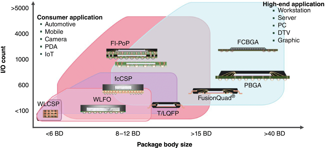
Figure 3.7 Product package position for WLP and FC‐CSP [1].
Source: Courtesy of Amkor Technology, Inc.
3.3 Manufacturing Process Flow and BOM
FO‐WLP is generated in four major process blocks: reconstitution, which itself includes four major process steps; RDL; solder ball application and package singulation; and electrical test. In reconstitution, a tested wafer is sawn into separate components, while in parallel a double‐sided adhesive foil is attached to a carrier, typically by lamination. The adhesive foil is releasable and loses its stickiness by addition of energy (e.g. by heating). Then, tested known good die are picked from the singulated silicon wafer and are placed on sticky tape on the carrier. The die spacing defines the fan‐out area of the package. It can be small or large, depending on the final package size required. Next, mold compound in liquid, granular, or sheet format is applied onto the die. By using a compression molding process, the die are embedded into mold compound, filling the gaps between the die and forming the artificial wafer. The artificial wafer consists of silicon die and mold compound and is round like a semiconductor wafer with a notch or flat as rotation indication. The wafer is cured. Finally, the foil is debonded from the carrier. Figure 3.8 shows the reconstitution process flow of eWLB as an example. Other technologies have similar process flows.
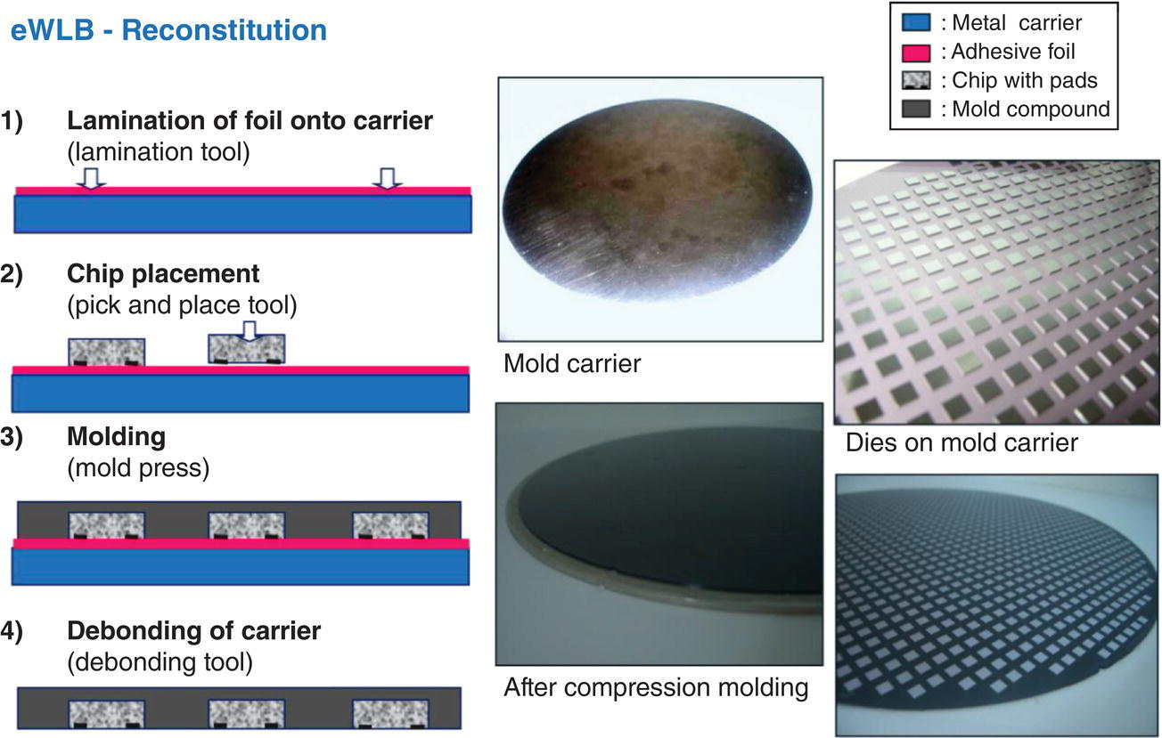
Figure 3.8 Reconstitution of artificial wafer [2].
Source: Reproduced with permission of IEEE.
The typical process blocks of FO‐WLP technologies are shown in Figure 3.9. After the reconstitution, the artificial wafer is processed like WLP. A dielectric is applied by spin coating. Due to the limited temperature stability of the mold compound, a low temperature cure material is used (see chapters later in this book on low temperature cure dielectric materials). Imaging vias in the dielectric can be done by laser direct imaging (LDI) or lithography. In eWLB, lithographic stepper technology is used for the exposure of the dielectric layer. The vias are the openings in the dielectric above the pads of the die as well as in the dicing street.

Figure 3.9 eWLB cross section and process overview [2].
Source: Reproduced with permission of IEEE.
The RDL is applied using thin film technology. An adhesion promoter layer such as titanium or titanium–tungsten is applied using sputtering. Next, a copper seed layer is sputtered. A plating resist is applied by spin coating and is photoimaged to create the pattern for the RDL circuitry. In eWLB, a stepper technology is used for the exposure of the plating resist. After development of the resist, the copper redistribution is now plated on the seed layer in the openings of the plating resist. Thicknesses between 4 and 8 μm of copper layer are typical. Next, the plating resist is removed and the two seed layers are etched away one after the other.
The last dielectric layer covers the redistribution and defines the landing pads for solder balls. Then the solder ball application is done at wafer level. Flux is applied onto the landing pads, typically in a printing process with a stencil, and then preformed solder balls, which are available in many different diameters, are rolled into openings of a stencil above the positions of printed flux. The solder balls stick in the flux and the wafer is transported into a reflow furnace. After melting, the solder balls are connected to the redistribution.
Finally, wafer thinning by standard wafer grinding and polishing is completed, and then laser marking on the die backside, reconstituted wafer dicing, and final test of the components. Figure 3.10 shows a cross section of the final package.
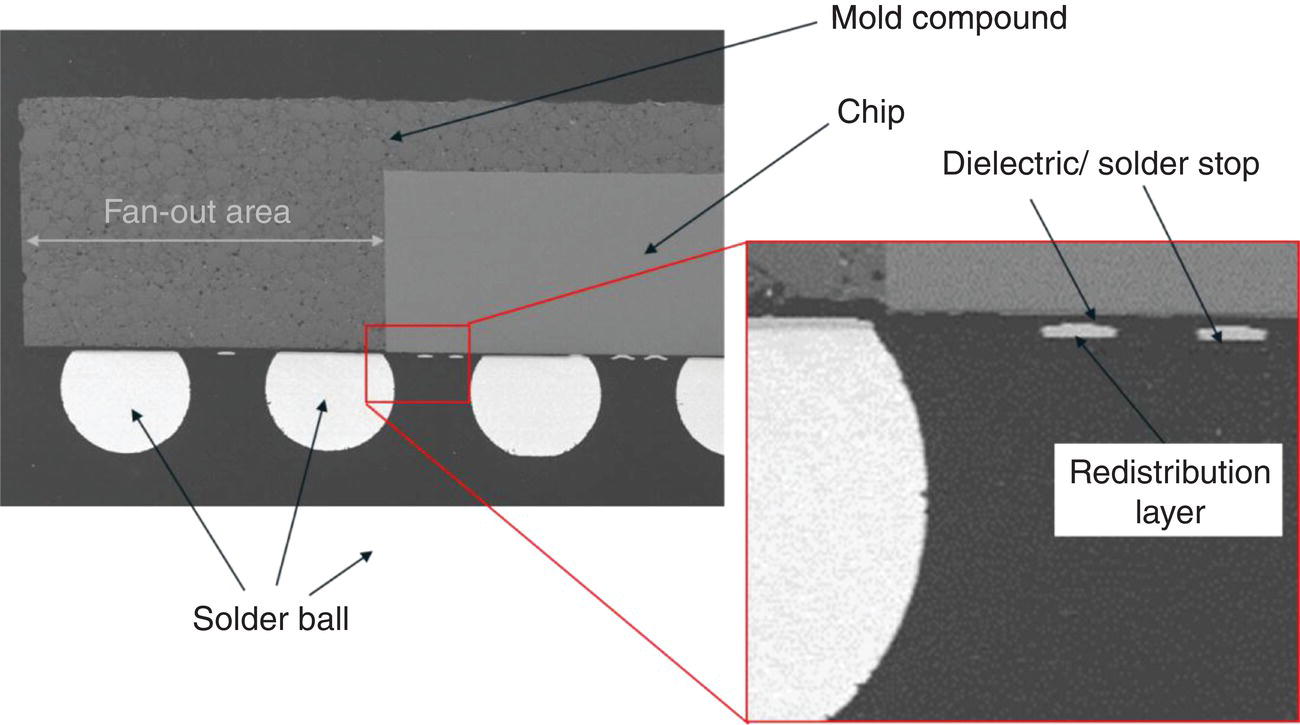
Figure 3.10 Cross section of eWLB.
The bill of materials (BOM) for FO‐WLP contains the following basic materials:
| Material | Function | Typical material class |
| Mold compound | Fan‐out area, die protection | Liquid epoxy mold compound, granular epoxy mold compound |
| Dielectric layer | Isolation, mechanical buffering | Polyimide, epoxy, silicone |
| Redistribution | Electrical contact, ball pad, passive structures | Electroplated copper |
| Solder stop | Isolation, ball pad definition | Polyimide, epoxy, silicone |
| Under‐bump metallization | Solder ball landing pad | Electroplated copper or copper/nickel/gold |
| Solder ball | Customer interface, second‐level interconnect element | Lead‐free SAC (tin, silver, copper) with different contents (e.g. SAC105, SAC305, etc.) |
3.4 System Integration Capability
FO‐WLP is best suited for system integration: both horizontal multi‐die packages as well as for vertical stacked integration of active and passive components. SiP applications are realized by placing two, three, or more active die in one package, for example, baseband, power management unit, and an RF module. Also, the integration of passive devices like surface‐mount devices (SMD) and integrated passive devices (IPD) saves significant space on the application board and improves electrical system performance. Multiple components can be placed side‐by‐side above the die, or face‐to‐face on the active die area without increasing z‐height. Furthermore coils, capacitors, resistors, and especially antennas can be directly formed using the RDL. Coils and antennas in particular can be realized in the fan‐out area with an excellent quality factor since they are isolated over mold compound instead of over the die.
Side‐by‐side integration is already well known in the industry for classical package technologies. FO‐WLP can provide performance and dimensional advantages due to the fine width and space of the redistribution lines and resulting high packaging density. Multiple die can easily be placed into the mold compound, next to each other and very close. Die distances at and below 50 μm have been achieved to date. Die of different front‐end nodes can be used, as well as active or passive components. Figure 3.11 shows a two‐die test vehicle with a die‐to‐die distance of 300 μm. The redistribution connects the two die as well as connecting to the solder balls. This way, multiple connections with very tight pitches can be realized.

Figure 3.11 Side‐by‐side approach of FO‐WLP.
The example above is only one flavor of realized side‐by‐side FO‐WLP. In order to achieve a higher interconnect density, different package types have been developed. Amkor’s silicon wafer integrated fan‐out technology (SWIFT) is one example of a chip‐first, RDL‐first fan‐out multi‐die package (see Figure 3.12) [3]. With its fine feature photolithography and thin film dielectrics, SWIFT bridges the gap between TSV and traditional wafer‐level FO‐WLP. Since very tight pitches can be realized, SWIFT offers strong improvements in form factor, signal integrity, power distribution, and thermal performance compared with classical packages. SWIFT incorporates an RDL‐first process, which means that the RDL are generated before the silicon is attached.

Figure 3.12 Side‐by‐side approach of SWIFT [3].
Source: Courtesy of Amkor Technology, Inc.
FO‐WLP is also suitable to be used for PoP stacking. Typically, a memory package is placed on the backside of a bottom package, which often contains a processor or another logic die. Top‐to‐bottom connections can be realized by laser‐drilled through‐mold vias or by placing prefabricated contact bars in the fan‐out area of the bottom die. Also, by implementing a backside RDL with landing pads and connection to the frontside, an area array can be achieved. The very stable coplanarity over temperature is another big advantage of this technology for package stacking.
The most prominent example for a PoP package is TSMC’s InFO package. InFO is a chip‐first face‐up FO‐WLP using copper pillars to provide 3D interconnections to connect the bottom RDL circuitry to the topside of the package, so a DRAM package can be attached on top of the applications processor for a mobile phone. Figure 3.14 shows another example of system integration in FO‐WLP. Oscillators as well as discrete passive components of different dimensions (e.g. 0201 or 01005) are embedded in the mold compound next to each other. Also, components from tape and reel can be picked and placed onto the mold carrier next to silicon die, as shown in Figure 3.13.

Figure 3.13 Heterogeneous system integration [3].
Source: Reproduced with permission of Amkor Technology, Inc.
The integration of MEMS or nanoelectromechanical systems (NEMS) components often requires special packaging solutions. MEMS structures often are sensitive to mechanical stress in production or later in application and also often require mechanical decoupling, shielding, or hermetic housings. FO‐WLP offers special capabilities for those applications. For example, a pressure sensor with a mechanically sensitive membrane can be embedded in mold compound close to an ASIC, but may not be connected to the board by solder balls, as indicated in the sketch in Figure 3.14. This way, the sensitive sensor is decoupled from the mechanical mismatch of CTE between the die and package and board. ASIC and MEMS are integrated, which requires codesign, a design focusing not only on the single die but also on the design of the complete system. Products like this actually are under development, not in high volume production.
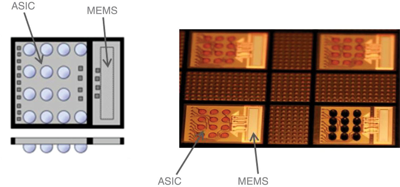
Figure 3.14 Heterogeneous system integration of ASIC and MEMS.
3.5 Manufacturing Format and Scalability
FO‐WLP in high volume manufacturing today is typically produced in 300 mm wafer format. Some users still produce in 200 mm wafer format due to availability of the production line, but the low economy of scale of this smaller size is not cost competitive. One supplier of FO‐WLP has moved to 330 mm round format after adaptation of toolings and handling systems. The additional economy of scale lowers the production cost.
A strong trend of the recent past is the move to panel format for low‐end FO‐WLP. Multiple companies are moving to rectangular substrate formats in order to increase the economy of scale further and therefore reduce packaging cost. Table 3.1 shows the area scaling factors for different dimensions. So far, no standards have been set for this production technology. The first panel technologies in high volume manufacturing are expected in 2018.
Table 3.1 Formats and area scaling factors for different substrate formats.
Source: Reproduced with permission of IEEE.
| Format | Dimensions | Area scaling factor |
| Round | 300 mm Ø | 1× |
| 300 × 300 mm2 | 1.64× | |
| Square | 500 × 500 mm2 | 4.54× |
| 600 × 600 mm2 | 6.5× |
3.6 Package Performance
As indicated earlier, FO‐WLP offers many advantages in comparison with traditional WB‐CSP or FC‐CSP. In this section, the warpage behavior and the electrical and thermal performance of different package platforms will be compared. The lack of warpage change over temperature of FO‐WLP is a distinct advantage. While the warpage of the FO‐WLP changes little with temperature, strong and very strong warpage change over temperature is documented for embedded die and for FC‐CSP [4]. This can be a strong advantage for testing, assembly, reliability, or 3D technologies, for example, PoP. For high yield package assembly or PoP stacking, warpage of the package is critical. If the warpage is too large, open solder joints may occur between the bottom package and the board or between the two stacked packages. Therefore, not only warpage at room temperature is a concern, but also the warpage at solder reflow temperatures (up to 260 °C) should be considered. As a result, warpage control at both temperature extremes is critical for package assembly [4].
From an electrical point of view, FO‐WLP shows lower RLC package parasitics (resistance, inductance, and capacitance) compared with WB‐CSP and FC‐CSP. This is mainly because FO‐WLP has shorter interconnects due to its substrate‐less design. In Figure 3.15, package resistance and inductance of the interconnects from die to package and the package construction are compared for the different packaging platforms in simulation. Resistance and inductance values have been extracted from the simulation. For the comparison, packages with the same functionality have been chosen according to existing package design rules. The simulation of the interconnect compares aluminum wire bond with a solder‐bumped flip‐chip interconnect on a two‐layer substrate with a one‐layer RDL for the FO‐WLP.

Figure 3.15 Electrical performance comparison (resistance, inductance) [5].
The direct current (DC) resistance and the electrical resistance at 5 GHz of the wire‐bonded package is a factor of 10 higher than the resistance of the flip‐chip interconnect with solder bump with a diameter of 150 μm. The electrical resistance of the FO‐WLP interconnect is even reduced by a factor of 2 compared with the flip‐chip interconnection. For the inductance, of the three interconnects, a similar picture is seen. It is reduced for the flip‐chip interconnect compared with the wire‐bond variant, but again improved by the FO‐WLP due to the laminate substrate‐less design. Translated to a potential package solution, this leads to lowest electrical resistance and inductance for the FO‐WLP.
Comparing the thermal performance between WB‐CSP, FC‐CSP, and FO‐WLP leads to a similar picture as the electrical performance comparison (see Figure 3.16). Simulations of the thermal resistivity (Rth) consider constant power dissipation for all packages and a constant die size for all platforms. In Figure 3.16, a comparison of Rth is shown. A wire‐bond BGA with two‐layer substrate, a flip‐chip package with two‐layer substrate, and an FO‐WLP with one‐layer redistribution are compared in simulation. The simulation model contains constant die sizes, and package size is chosen according to standard package design rules. FO‐WLP shows better thermal performance compared with WB‐CSP and FC‐CSP because of the thinner package, the absence of an isolating substrate, and less interfaces between the die and the heat sink (board).
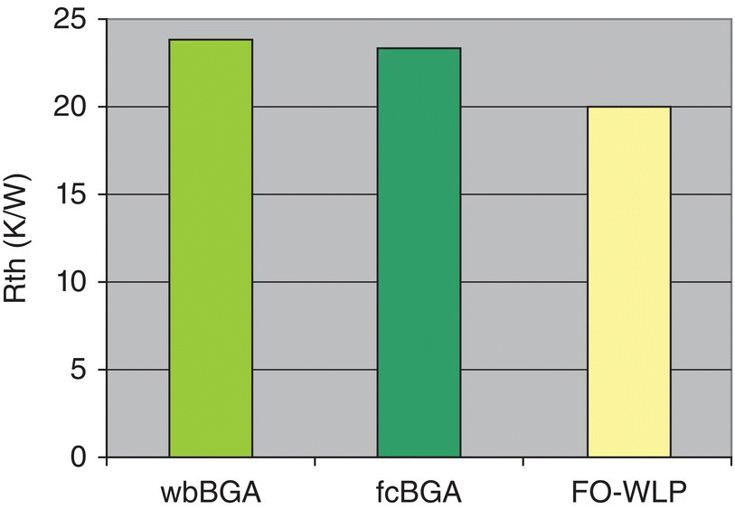
Figure 3.16 Thermal performance comparison.
3.7 Robustness and Reliability Data
The excellent electrical and thermal performance of FO‐WLP is caused by short and direct interconnects, the absence of a board with additional thermal resistance and electrical performance reduction, and a reduced number of interconnects. This causes a performance advantage, but it causes challenges as well. The package is directly connected to a PCB, without buffering layers. Therefore, the mismatch of CTE between the silicon die, the mold body, and the PCB has to be compensated by the solder balls and a thin dielectric layer. The major hurdle for WLP is the TCoB, where the component is attached to a standardized PCB and exposed to thermal cycling (e.g. −40 to 125 °C).
Package boundary conditions like die and package size, package thickness, number of solder balls, solder ball material and size, and many more influence the reliability results. Table 3.2 shows an overview of typical reliability tests for consumer products. In this case, the following boundary test vehicle conditions have been used:
Table 3.2 Overview consumer reliability performance of FO‐WLP.
| Stress test | Standard/spec | Pass criteria |
| Moisture sensitivity level (MSL) | EIA/J‐STD‐020C (Level 1) |
MSL 1 |
| High temperature storage (HTS) | JESD22‐A103 (Ta: 150 °C) |
1000 h |
| Temperature cycling (TC) | JESD22‐A104 (Cond B: 55–125 °C) Preconditioned (Level 1; Tr: 260 °C) |
1000× 1500× |
| Unbiased HAST (uHAST) | JESD22‐A118 (Cond A: 130 °C/85% RH) Preconditioned (Level 1; Tr: 260 °C) |
96 h 188 h |
| Temperature humidity bias (THB) | JESD22‐A101 (85 °C/85% RH, VCC) |
1000 h |
| Temperature cycling on board (TCoB JEDEC) | IPC 97‐01 (−40 °C/+125 °C, 1 cy h−1) |
500× 1000× |
| Temperature cycling on board (TCoB NOKIA) | NOKIA spec. (−40 °C/+125 °C, 2 cy h−1) |
FF > 500 cycles |
| Drop test | JESD22‐B111 | <10% fails at 20 drops |
| Package size | 9.25 mm × 8.80 mm |
| Die size | 5.28 mm × 5.62 mm |
| Ball pitch | 0.5 mm BGA pitch |
| Construction | Single die, one‐layer‐Cu‐RDL, polyimide dielectric, no UBM, 122 solder balls |
The described FO‐WLP passed all required tests. This allows a move toward automotive applications with higher reliability requirements.
FO‐WLP has entered the automotive market for radar applications. The package is best suited for high frequency applications due to the thin film RDL with very reproducible properties and low parasitics. Also, the solder ball interconnects can be placed on the fan‐out area, an important feature for electrical performance at high frequencies. Figure 3.17 shows the 77 GHz radar component in eWLB package technology. The die in the center of the package contains only four thermal balls, and all other interconnects are placed over the fan‐out area. It can be seen that a redundant ball concept is used and multiple solder balls from center to edge are connected by the RDL. This way, all solder balls carry the same signal. During temperature cycling, stress will occur in the solder balls due to the mismatch of CTE of the package (3–9 ppm °C−1) and the PCB (14–20 ppm °C−1). The highest stress will occur in the solder balls with the largest distance to the center of the package or distance from neutral point (DNP). This stress will cause the solder balls with largest DNP to crack first, but redundant balls are continuing to transfer the signals. With the redundant ball concept, connected solder balls can take over the transmission of the signal with no impact on the electrical functionality due to the cracked solder ball. This way, the redundant ball concept improves the TCoB performance strongly.

Figure 3.17 eWLB 77 GHz radar package.
FO‐WLP passed automotive standard AEC‐Q100 Grade 1 for advanced driver assistance systems (ADAS). Table 3.3 gives an overview of the reliability test results.
Table 3.3 Overview automotive reliability performance of FO‐WLP.
| Test | Conditions | Criteria | Result |
| Temperature cycle | −65 °C/+150 °C | 1000 cycles | Pass continued up to 1500 cycles |
| Temperature cycle on board | −40 °C/+125 °C | 1300 cycles | Pass 1st fail at 2215 cycles/first 6 fails up to 2500 cycles |
| Drop test | JEDEC JESD22‐B111 |
Pass 1st fail at 120 drops | |
| uHAST | 130 °C/85% | 192 h | Pass |
| HTS | 150 °C/175 °C | 2000 h 1000 h |
Pass |
3.8 Electrical Test Considerations
The proof of electrical functionality is an important milestone for any package platform. CSP packages are tested after singulation into discrete packages. This flow is indicated in Figure 3.18 as Flow 1. A wafer from the front end is tested on wafer level and diced after test. Functional die are then assembled in the package. After package singulation, the package test is performed. Defects caused by dicing will be testable in this flow. For FO‐WLP, a reconstituted wafer test is possible as well, as indicated in Flow 2 of Figure 3.18. However, FO‐WLP can also be tested after package singulation like CSP (Flow 1) as shown in Flow 3.
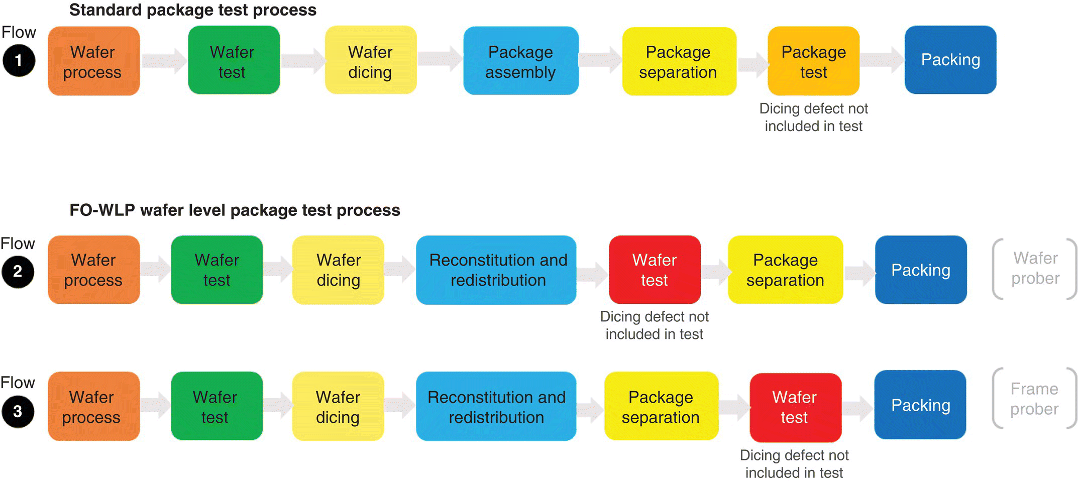
Figure 3.18 Electrical testing flows for (1) CSP and (2) and (3) for FO‐WLP.
Flow 2 is a wafer‐based test flow. The front‐end wafer is tested and diced. The wafer‐level testing is important to find known good die for reconstitution. This way, the reconstituted wafer starts with typically 100% yield. After the reconstitution and the application of dielectric, RDL, and solder balls, the reconstituted wafer can be tested using a wafer prober. After this, package singulation is performed. Due to the singulation after testing, potential defects due to the singulation process are not detected. Since package singulation is done through mold compound and not through silicon, this is seen as low critical. In order to avoid discussion of yield loss due to dicing defects, frame prober testing can be carried out. It follows the same steps as Flow 2, but package singulation is done prior to the final testing. This is then done with a frame prober on the dicing tape/frame, and it also indicates potential defects from the singulation process.
3.9 Applications and Markets
End customer acceptance of new package types and multi‐sourcing strategies impede the introduction of new packaging technologies like FO‐WLP. Most important, packaging cost for large FO‐WLP is still high. Packaging cost reduction is a major target for FO‐WLP technologies at the low end. Therefore, the switch from round wafer format to rectangular panel format using cost‐effective PCB process technologies will be a next step in this area. Even with a PCB‐technology‐related lower pattern density and a possible need for additional RDL, the lower process costs and the much higher process economy of scale will improve the cost per package significantly.
Continuous shrinking of the silicon nodes leads either to reduced die sizes or to higher I/O counts due to increased functionality. In both cases, a need to switch from the die‐size‐limited WLP to the much more flexible FO‐WLP technology arises. Therefore, the future focus for high‐end FO‐WLP will move from the single‐die package, using one RDL, to highly integrated SiP, using multiple routing layers on the package frontside and for package stacking technology (PoP), also additional routing layers on the package backside. This will speed up the integration of sensors and MEMS close to the AP or at least to bundled modules.
References
- 1 Kroehnert, S. (2017). Fan‐Out SiP Solutions – WLSiP and WL3D. Inaugural Conference and Exhibition on SYSTEM‐IN‐PACKAGE (SiP) TECHNOLOGY, Doubletree Sonoma Wine Country, Sonoma, California, USA (27–29 June).
- 2 Meyer, Th., Pressel, K., Ofner, G., and Römer, B. (2010). System integration with eWLB. Electronic System‐Integration Technology Conference (ESTC), Berlin, Germany (2010).
- 3 Huemöller, R. (2015). Amkor’s SLIM & SWIFT Package Technology. Semicon Taiwan.
- 4 Prashant, M., Liu, K., Jin, Y. et al. (2010). Next generation eWLB (embedded wafer level BGA) packaging. Electronics Packaging Technology Conference (EPTC), Singapore (2010).
- 5 Pressel, K., Beer, G., and Meyer, T., (2010). Embedded wafer level ball grid array (eWLB) technology for system integration. IEEE CPMT Symposium, Japan.