
17
Process and Equipment for eWLB: Chip Embedding by Molding
Edward Fürgut1, Hirohito Oshimori2, and Hiroaki Yamagishi2
1 Infineon Technologies AG
2 Apic Yamada Corporation
17.1 Introduction
Today, semiconductor devices with rapidly changing features are the basis for applications that deliver comfort, communication, mobility, environmental, and medical care. New requirements for reliability or environmental constraints are the driving factors to develop new materials, processes, and equipment. During recent years, molding process development has became increasingly important. The development of new encapsulation methods including processes and materials allowed manufacturing of high performance, reliable, and cost‐efficient microelectronic devices.
In this chapter a short history of molding is provided, which highlights that the introduction of compression molding was a major change for semiconductor assembly and packaging. Why compression molding was the key for the implementation of the innovative extended wafer‐level ball grid array (eWLB) technology in 2006 is described. Next, the compression molding process for the new fan‐out technology and the principle challenges are introduced. Finally, processing solutions that enable fully automatic compression molding with newly developed equipment are described. The new compression molding system was a significant breakthrough in semiconductor assembly and packaging technology. Conclusions and next steps complete this chapter.
17.2 Historical Background Molding
Up until the 1960s, hermetically sealed metal and glass packages were standard. In these early years of microelectronics, encapsulation by liquid glob top material was used to protect wire‐bonded semiconductor devices from environmental influences [1]. Encapsulation material improvements, especially in ionic purity, mechanical properties, thermal stability, and minimization of hazardous contaminants, resulted in enhanced long‐term device reliability and performance.
In the 1980s, transfer molding was introduced for microelectronic packaging (see Figure 17.1). During transfer molding, the encapsulation material is transferred from the pot into the cavity by plunger pressure. The material is usually in the form of a pellet. In the early days of transfer molding, cost‐efficient manufacturing was considered a higher priority than component reliability. The transfer molding method was first possible with mono plunger systems based on a hydraulic press. These mono plunger mold tools were designed and manufactured mainly by semiconductor companies.
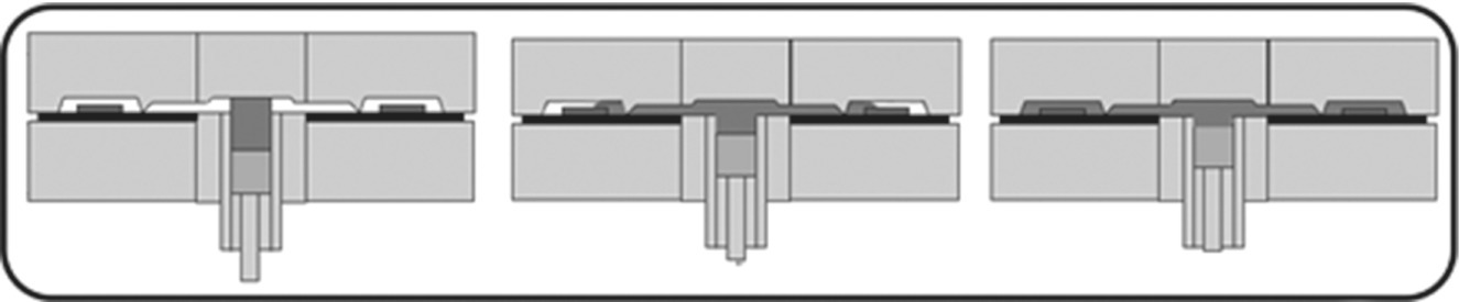
Figure 17.1 Transfer molding process schemes for single cavity lead‐frame packages showing three process steps: (left) pellet melting inside pot, (middle) mold flow through runners and gates, and (right) complete mold filling of all mold tool cavities.
In the late 1980s, new requirements in the semiconductor industry, e.g. higher quality and yield combined with the request for miniaturization and increased functionalities, caused the need for the development of multi‐plunger mold tools with a toggle press. These multi‐plunger mold tools were designed and produced at pure toolmakers because of their high complexity. The mold tool is the main part of the process; therefore some of the former pure toolmakers are today’s full equipment suppliers. Because of the proven advantages in terms of productivity, material waste minimization, and proper maintenance efforts, the transfer molding process with multi‐plunger systems became a standard [1]. During the 1990s, the need to encapsulate larger and thinner chips showed the limit of transfer molding for long material flow distances. Thus, new encapsulation methods were required.
In 1997, Apic Yamada introduced compression molding for encapsulation of large and thin cavities using liquid molding compound (LMC). This latest innovation of introducing LMC and compression molding in semiconductor encapsulation was first used for wafer backside coating. The introduction of compression molding was a major change in assembly and packaging technology. The origin of compression molding was the bakery industry followed by the general plastic industry. The plastic industry used compression molding first to replace metal with plastic parts. The typical applications were to manufacture parts such as rubber boots, scoops, fenders, and spoilers, as well as smaller and more complex parts.
The compression molding concept combines compound forming and pressure in a mold cavity. The compound is placed directly into a heated mold cavity. During closing and applying force, the compound is softened and formed by the mold cavity [2]. Figure 17.2 schematically shows the compression molding process.

Figure 17.2 Compression molding scheme of a molded array package (MAP) based on substrate: (left) the molding compound is deposited on the chips that are fixed to a carrier, (middle) the unmolded device is placed on the bottom mold tool, and (right) the liquid molding compound fills the space between the chips fixed to the carrier and the cavity to shape the MAP.
In the next chapter the importance of compression molding for the eWLB technology (fan‐out WLP) is demonstrated.
17.3 The Molded Wafer Idea: Key for the Fan‐Out eWLB Technology
For standard wafer‐level packaging (WLP), solder balls are mounted on semiconductor wafers. These wafers with solder balls are then diced and mounted on a printed circuit board. Before solder ball mount, an additional thin film redistribution layer (RDL) can be added (see Figure 17.3). These technologies successfully entered into the semiconductor industry mainly for small chips (< 5 mm × 5 mm). The major obstacle for WLP was the transfer of the high density pin count (I/O) on chip level to the printed circuit board (PCB). Due to the large difference in coefficient of thermal expansion (CTE) between silicon (3 ppm K−1) and the PCB (typically 14–20 ppm K−1), chips with an area larger than 5 mm × 5 mm as a rule of thumb require underfill to achieve sufficient board reliability. Thus, we need a fan‐out area for small and high pin count chips. This leads to the fan‐out eWLB package as shown in Figures 17.3 and 17.4.
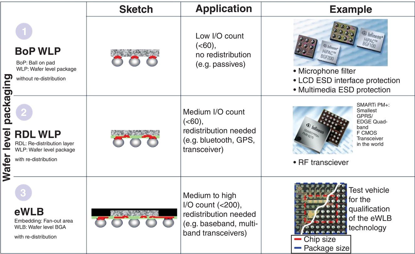
Figure 17.3 Comparison of ball on passivation (no RDL) WLP, RDL WLP, and fan‐out eWLB technologies.
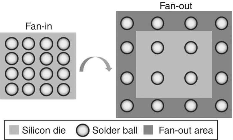
Figure 17.4 From fan‐in to fan‐out technology.
The fan‐out eWLB technology fills the interconnect gap, allowing for the ongoing miniaturization of the pitch on the chip and the typically non‐changing pitch on the application board [3].
Infineon was the first company to successfully investigate and introduce a fan‐out eWLB package into the market. The basic idea of this new package concept was to dice the wafer into single chips and embed these chips in molding compound to form a reconstituted molded wafer. Figure 17.5 shows on the left the four main processes for creating the reconfigured wafer: tape lamination on carrier, chip placement, encapsulation (molding), and debonding. On the right of Figure 17.5, an image of the final reconfigured wafer with the die embedded in mold compound is demonstrated [4].

Figure 17.5 The four main processes for creating the reconfigured wafer via compression molding: tape lamination on carrier, chip placement, encapsulation and debonding (left) and image of the final reconfigured wafer with the die embedded in molding compound (right).
This molded wafer (reconfigured wafer) is the core of the new fan‐out eWLB technology. The introduction of this molded wafer applying compression molding led to the launch of fan‐out WLP. Further details on compression molding to manufacture the molded wafer are presented in the next section.
The new eWLB packaging concept based on a fan‐out molded wafer enables new design opportunities in comparison with WLP. The concept offers the following main advantages:
- Integration of chips with different sizes in a standardized predefined package (example: memory chips of different generations).
- Embedding of different chips side‐by‐side into one system in a package (SiP).
- Elimination of bump and wire bond to improve the electrical and thermal performance of the package.
SiP using eWLB technology provides products with high integration potential capability, design flexibility, and high interconnection density. Figure 17.6 shows a plot of the chip size versus package size [5]. The advantage of the molding process is the capability to cover a large range of chip and package sizes. A new package platform is generated, which also allows multi‐chip integration. The following Figure 17.6 shows the dimension restriction of WLP in comparison with the dimension flexibility of eWLB. The package and chip have the same size (see the WLP line with slope 1) for the WLP package platform. The eWLB package platform offers improved flexibility with respect to chip size and multi‐chip side‐by‐side integration (see the application below the WLB line, e.g. with slope <1). A multi‐chip solution with 3D integration is required to address the slope >1.
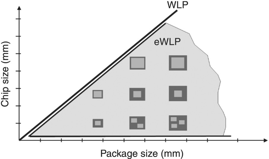
Figure 17.6 Flexibility of the eWLB package platform in comparison with the limitation of the WLP package platform.
Wafer front‐end manufacturing has a significantly higher degree of automation compared with assembly and packaging manufacturing (back end). The development target was an encapsulation process with the highest possible automation to enable a manufacturing environment similar to front‐end production. The high degree of automation for the eWLB package enables a high manufacturing yield in spite of the significantly increased number of process steps compared with typical back‐end manufacturing.
The existing manufacturing methods within the semiconductor industry did not provide the following required features to fabricate a molded wafer:
- Temporary bonding of chips.
- Molded wafer with thermal stability.
- Molded wafer with identical dimension to SEMI specification [6].
Thus, a complete new manufacturing concept and encapsulation process had to be developed. Different encapsulation methods as shown in Figure 17.7 were considered.
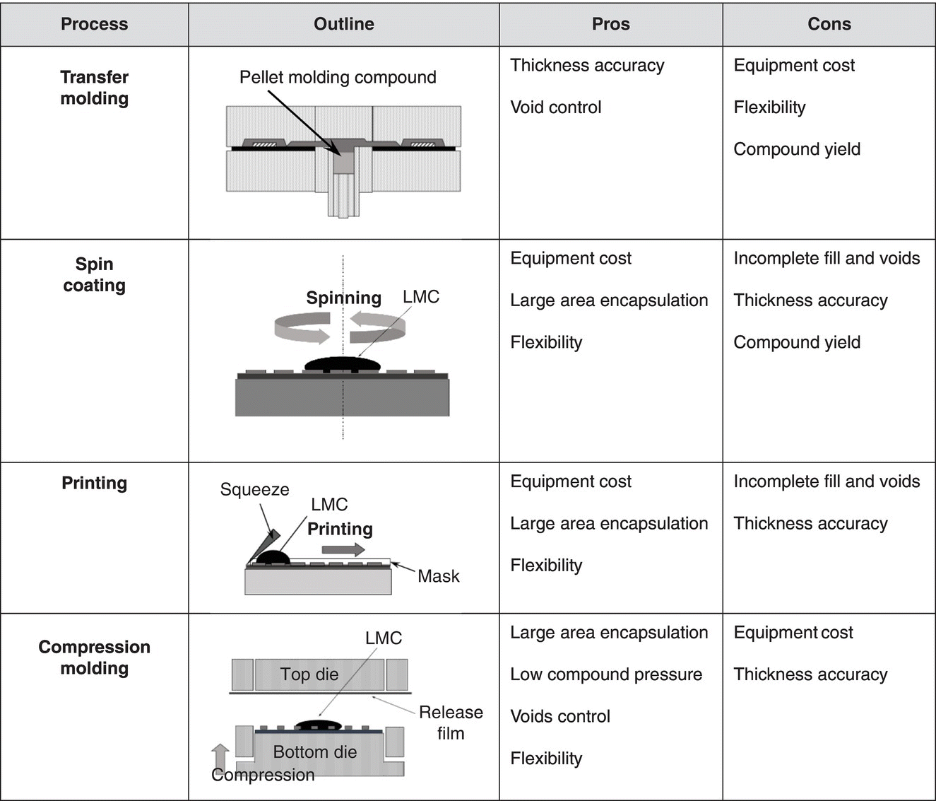
Figure 17.7 Molded wafer encapsulation methods with their pros and cons.
The investigation and evaluation of the complex and new manufacturing process required many years of systematic feasibility studies in materials, processes, and automation. This included, for example, careful studies of die shift, wafer warpage, large and thin wafers, etc. Figure 17.8 shows an example of a die‐shift optimization; Figure 17.9 shows an example of a warpage optimization [5].

Figure 17.8 eWLB die shift before (left side) and after (right side) optimization.
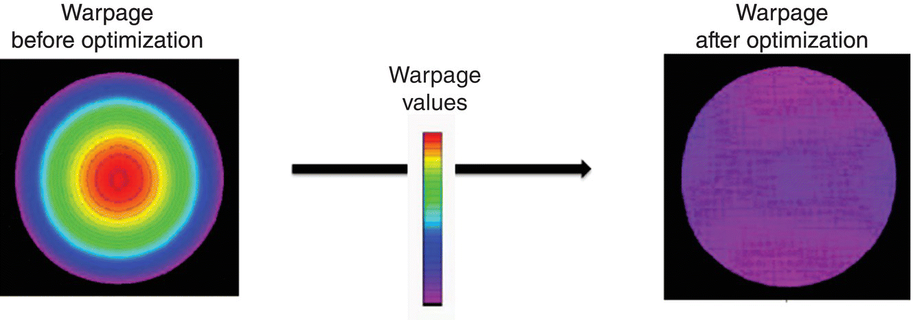
Figure 17.9 eWLB warpage before (left side) and after (right side) optimization (left side).
Figure 17.8 demonstrates the eWLB die shift before and after optimization. The die shift before optimization (left side) increases from center to wafer edge:
The die shift is related to mold area to chip area ratio. The die shift after optimization (right side) is improved due to the linear die‐shift correction:
The model for Ccorrection is a function for chip area to molding area ratio [5].
Figure 17.9 shows the eWLB warpage before (left side) and after (right side) optimization. The molding compound area to chip area ratio influences the wafer warpage (CTE mismatch). The warpage after optimization shows the wafer warpage of improved molding compound (low CTE in combination with low E‐modulus). The molding and debonding is also optimized to achieve a low warpage [5].
Based on the research, the following main topics were identified as crucial:
- Temporary rigid carrier (carrier system)
- LMC
- Compression molding process
A new manufacturing concept to encapsulate chips in a molded wafer was developed. Figure 17.10 schematically illustrates the cross‐sectional scheme of a molded wafer and the carrier system [5].
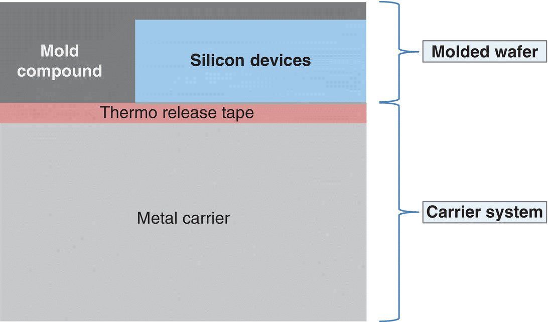
Figure 17.10 Schematic cross section of a molded wafer with carrier system.
The manufacturing concept is based on a carrier system that consists of a metal carrier and a thermal release tape (see Figure 17.10). The silicon devices are placed face‐down on the thermal release tape prior to compression molding with LMC. Below, the two main parts are described in detail, the carrier system and the molded wafer, as well as the debonding processes.
17.3.1 Carrier System
The carrier system consists of two components, the metal carrier and the thermal release tape. The CTE of the metal carrier and molded wafer, which consists of the LMC and silicon die, needs to be properly adjusted to each other. The CTE of LMC is in the range of 6–14 ppm K−1, whereas the CTE of the silicon die is about 3 ppm K−1. Therefore, thermal expansion of the molded wafer may be described by an effective CTE of 4–12 ppm K−1. Additional properties required of the metal carrier are handling robustness and low warpage.
The thermal release tape fixes the chips during molding and defines the active side of the molded wafer. The thermal release tape is a double‐sided adhesion tape with different properties on both sides. On one side, a thin layer with pressure‐sensitive adhesive glue is applied. On the opposite side, a thin layer with thermal release adhesion glue is applied. Figure 17.11 shows a cross‐sectional scheme of a thermal release tape that is a key material for the eWLB manufacturing concept.
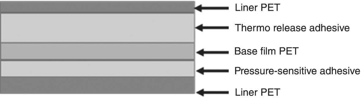
Figure 17.11 Cross‐sectional scheme of the thermal release tape; multiple layers are required for the tape processing (lamination).
The unique tape function is called thermal release, which means a high adhesive adhesion (fixing of the die during molding) is changed to no or very low adhesive adhesion (debonding of the carrier system) at a defined temperature. Figure 17.12 shows the adhesion force of a thermal release adhesive glue layer in relation to the heat treatment temperature.
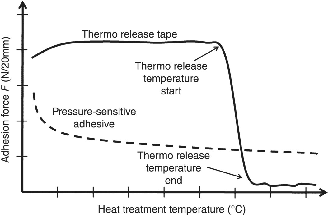
Figure 17.12 Adhesion force of a thermal release glue and a pressure‐sensitive glue in relation to the heat treatment temperature.
The thermal release temperature must be above the molding and post mold curing (PMC) temperature to avoid any separation or delamination of the thermal release tape before debonding. The debonding of the molded wafer from the carrier system is done by a temperature process. To enable a mechanical stress‐free separation of the molded wafer from the carrier, the debonding temperature has to be higher than the thermal release temperature.
17.3.2 Molded Wafer
The molded wafer consists of LMC and silicon die. The semiconductor chips are placed either face‐down or face‐up on the carrier system (metal carrier and thermal release tape). The opportunity to place only the known good die (KGD) enables an increased package yield especially in multi‐chip configurations. Key factors are position accuracy between the chips and accuracy of the whole chip array. The carrier system consists of very accurate global alignment marks for pick and place and location holes to assure an accurate compression molding (see the Chapter 16 on pick and place by BESI). Figure 17.13 shows a 3D sketch (left) of the carrier system with the die after pick and place. On the right, the corresponding scheme of the cross section is shown.

Figure 17.13 Carrier system with chips after pick and place (left) and the corresponding cross‐sectional scheme of chips mounted face‐down on the carrier system (right).
The LMC is the key element of the molded wafer. The molded wafer consists of LMC and chips. Therefore the LMC properties define the molded wafer features like warpage and temperature stability. Compared with solid molding compounds, the LMC allows molding at lower temperatures. Details about the LMC material are described in the separate chapter of this book called “The Role of Liquid Molding Compounds in the Success of Fan‐Out Wafer Level Packaging Technology” by Nagase.
After placement of semiconductor chips onto the mold carrier system, the encapsulation process takes place. The molding starts with dispensing of the LMC in the center of the carrier system. In the next step, the compression molding takes place. This is followed by PMC to enhance LMC cross‐linking. Figure 17.14 shows the final molded wafer together with the carrier system below. The compression molding process will be explained in more detail in the subsequent sections.

Figure 17.14 3D sketch of the molded wafer together with the carrier system below (left) and a scheme of the cross section (right).
17.3.3 Debonding
After compression molding, the molded wafer will be separated from the carrier system using high temperature. The thermal release tape is removed at a defined high temperature. Figure 17.15 shows the molded wafer after debonding.
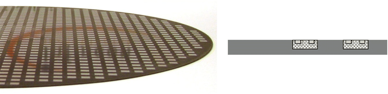
Figure 17.15 Photo of molded wafer after debonding (left) and the corresponding scheme of a molded wafer after debonding (right).
17.4 The Compression Molding Process
In this chapter, first the molding compound ingredients are introduced. Then, an overview of molding compound states of aggregation, cavity‐down and cavity‐up processing methods, molding compound preparation, temperature of compression molding, cavity filling, and mold release is given. This chapter concludes with a discussion of a comparison between transfer molding and compression molding capabilities.
17.4.1 Molding Compound Ingredients
Generally, the compression molding process can be performed with different polymer types like thermoplastic and thermoset materials. In the following, thermoset materials (molding compound) are the focus, which are most important for semiconductor packaging. The reasons are the required high temperatures (>175 °C) during package soldering and the high resistance to the environment. The molding compound consists of a multitude of different ingredients. The most important ingredients are the filler and resin, including hardener. In addition, optional ingredients are flame retardant, wax, adhesion promoter, catalyst, stress absorber, coloring agent, and others. Figure 17.16 shows typical ingredients of a molding compound, content (wt%), major functions, and typical agents.
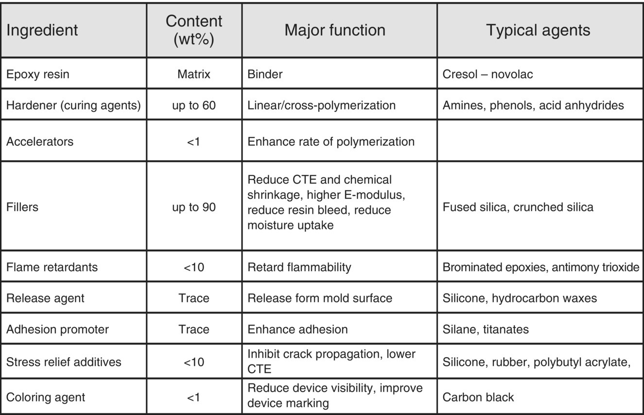
Figure 17.16 Ingredients of molding compounds that are used for encapsulation of semiconductor devices.
The mechanical properties like CTE and chemical shrinkage are influenced mainly by the filler content, which can be typically up to 90 wt%. The lowest CTE and chemical shrinkage requires the highest filler loading. The highest filler loading can be achieved by, for example, a tribology of spherical fillers. Figure 17.17 shows a cross section of a typical molding compound used for semiconductor packaging.

Figure 17.17 Cross section of a typical molding compound for semiconductor device application.
17.4.2 Molding Compound State of Aggregation
Compression molding is able to process molding compound with different states of aggregation. The mainly used states of aggregation for molding compounds are:
- Granulate molding compound (GMC)
- LMC
- Sheet molding compound (SMC)
The most commonly used material for compression molding in the back end is the GMC. This aggregation state is based on a solid molding compound. The liquid state of aggregation is used mainly in front‐end production for photomasks or polyimide passivation via spin coating. The sheet molding compound is well known for lamination in the PCB industry. Figure 17.18 shows the pros and cons of the three states of aggregation used for compression molding.
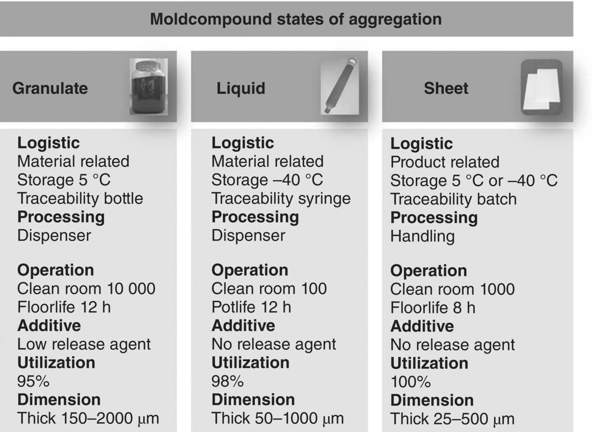
Figure 17.18 Molding compound states of aggregation for the compression molding process.
17.4.3 Processing Methods
Compression molding is a forming process, in which a plastic material is placed directly into a heated metal mold, then is softened by the heat, and is pressed into the mold cavity during mold closing (see Figure 17.19). The melting of the mold compound, forming, and final pressure is formed within the mold cavity. There are two different relevant methods for compression molding. Figure 17.19 shows the two different cavity molding process methods: cavity‐down and cavity‐up [2].
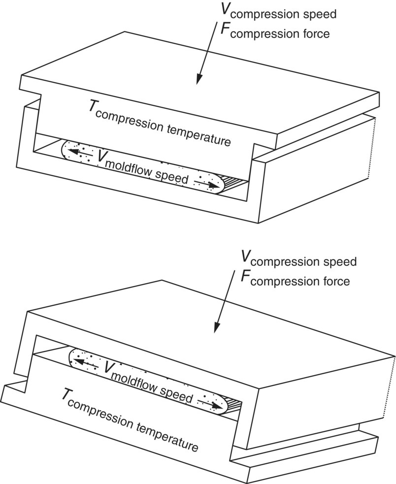
Figure 17.19 Compression molding methods cavity‐down (top) vs. cavity‐up (bottom).
The cavity‐down approach (Figure 17.19 left) places the molding compound directly into the bottom cavity. This approach is usually used for GMC and SMC. The reason is the fast handling capability that allows a direct placing into the bottom mold cavity. For this cavity‐down processing method, the carrier system is placed face‐down onto the top mold tool. The LMC is not used for the cavity‐down approach because of the tackiness of the uncured LMC and the relative long dispense time compared with GMC and SMC. The advantage of the cavity‐up approach is the possibility to distribute the molding compound over the area to minimize the mold flow. This method is also called compression molding by dipping. For the cavity‐up approach (Figure 17.19 right), the molding compound is placed onto the carrier system prior to compression, usually using LMC.
17.4.4 Molding Compound Preparation
Before the cavity filling process can start, certain procedures must be accomplished to prepare the molding compound to be molded. This typically involves dispensing, weighing, and placement of the molding compound [4]. In the past, these processes were mainly done manually. To ensure the required quality and throughput for the semiconductor market, the processing must be automated. Slight changes in the amount of the molding compound or displacement can lead to unacceptable results.
GMC is usually dispensed by a vibration mechanism. GMC can be easily distributed over the area to reduce mold‐filling issues. The GMC dust generation has to be managed by the molding equipment – especially by the dispenser. LMC is usually applied by a volume dispensing mechanism. Dispensing of GMC and LMC is time consuming. Therefore it is performed under room temperature before starting the molding process. A weight control loop is recommended to ensure accurate dispensing. The required molding compound weight (g) is implemented very precisely via software control. This is a main advantage compared with molding compound pellets that are used for transfer molding. The in situ weight control reduces the molding compound logistic complexity.
SMC can be tailored at the supplier or directly prior to the molding. Fully automatic handling is critical for SMC because of the flexibility and tackiness of the uncured sheet. The logistic complexity is increased due to product‐related variants, e.g. package thickness, chip dimension, etc. A variation of packages end up in several different SMC dimensions, for example, sheet thickness and sheet size. The molding compound volume in combination with the mold tool dimension defines the thickness of the compression molded part. The volume (cm3) is calculated by the product of the molding compound weight (g) and specific gravity (g cm−3). The deviation of molding compound volume results directly in a thickness deviation. In addition, the placement accuracy has a strong impact on the cavity filling behavior of the molding compound. Displacement of the SMC can result in incomplete fill (mold flow too long) or mold flash (mold flow too short).
Although the molding compound preparation step may seem trivial, it has the potential to be the root cause of many problems that appear throughout the entire molding process. This eventually leads to flaws in the molded part, for example, incomplete fill or internal voids [4]. Careful analysis and control of this step must be taken to assure that it does not create unnecessary problems like flow marks or molding compound segmentation. The molding compound preparation process has to be developed to have no impact to the cycle time of the overall compression molding process [2].
17.4.5 Compression Molding Temperature
Compression molding of thermosets uses a constant and homogeneous temperature within the top and bottom mold tool. The automatic temperature control technique of the mold tool ensures a surface temperature with low deviation. The surface temperature has to be controlled within ±5 °C or even ±3 °C to ensure a constant process quality. The molding temperature is related to the molding compound used. LMCs are usually processed in the range of 120–150 °C. GMCs are usually processed in the range of 150–190 °C.
The mold tool temperature combines two different functions. First, the mold tool temperature heats up the molded part and molding compound. The GMC requires melting (molding compound condition changes from solid to liquid) before it can be processed. The LMC can be processed at room temperature or between room temperature and the molding temperature. The viscosity of the molding compound is related to the temperature. Higher molding temperatures reduce the viscosity of the molding compound in the beginning and shortens the processing time due to the high degree of molding compound cross‐linking. A lower molding temperature enlarges the processing time and has a negative impact on the molding compound viscosity during mold filling. Figure 17.20 shows the viscosity of GMC and LMC materials vs. molding process time.

Figure 17.20 Viscosity of GMC and LMC material vs. molding process time.
Second, the mold tool temperature drives cross‐linking of the molding compound. The molding compound has to be sufficiently cross‐linked to enable proper release and robust handling. A higher molding temperature increases the cross‐linking speed of the molding compound. Thus, it reduces the required curing time. The mold tool curing time mainly determines the throughput of the whole molding process.
17.4.6 Cavity Filling During the Compression Molding Process
The solid molding compound (e.g. GMC) curing reaction and its mechanism of solidification create a network of tightly connected molecules. Molding compounds are typically placed on the bottom mold tool that is 175 °C at least and starts melting during the heating‐up process. The temperature can be seen as a catalyst for the curing process of any epoxy molding compounds. Once the molding compound is in full contact with the molding tool, the temperature transfer into the molding compound takes place immediately. The molding compound is a bi‐stage material. This means it includes a solid and a fluid state of aggregation. As a result of heating up the molding compound, the fluidic stage of the material ratio is drastically increased. This means the molding compound can be considered as fluid. This stage of aggregation is most important to be used for filling the cavity. The curing of the molding compound is continuously ongoing and strongly temperature dependent: commonly an increase of 10 °C will double the reaction speed, whereas a decrease of 10 °C will halve the reaction speed. As an effect, the molding compound changes its stage of aggregation back to solid where the ratio from fluid stage declines and the solid stage increases again. The molding compound viscosity curve is shown in Figure 17.20. The compression is related to the viscosity of the material and the molded area. A high‐end pressure is required to obtain a solid bulk molding compound with as little air entrapment as possible. LMC behaves differently from the GMC because of its low viscosity, and its workability at lower temperatures (even at room temperature) is already given. In addition, the LMC enables the whole encapsulation process to be driven at lower temperatures.
The flow speed of the molding compound has an important role for proper cavity filling. The optimized flowing speed of the material should be in the range of 1–10 mm s−1. The molding compound distribution prior to the filling of the cavity reduces the impact of molding compound flow speed significantly. This is mainly used for GMC and SMC with the cavity‐down concept. This is the so‐called “dipping” compression molding process concept.
The GMC distribution prior to material filling for cavity‐up has some limitations. Figure 17.21 shows the relation of compression speed versus molding compound flow speed. Especially for large and thin cavities, the compression needs to be specifically low to ensure an optimized molding compound flowability. The mold flow can be calculated as seen in Figure 17.21.
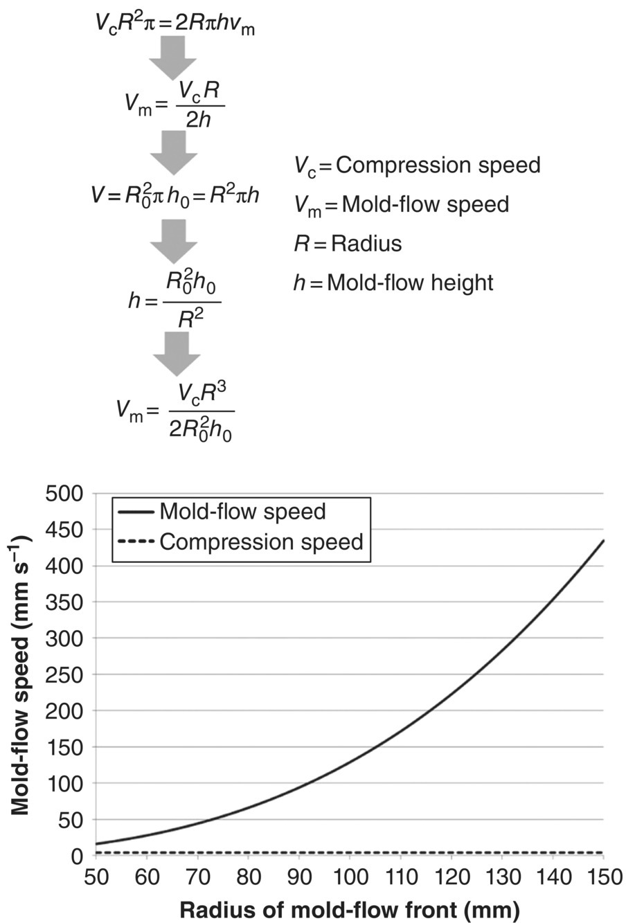
Figure 17.21 Mold flow speed vs. compression speed.
Another important parameter to ensure proper cavity filling is the end pressure. The final pressure reduces the internal and external voids and brings the molding compound into the final shape. In the compression molding process, the final pressure is in the range of 20–50 bar. Therefore it is significantly lower than in the transfer molding process where it is in the range of 50–100 bar. The lower final pressure results because the pressure is inserted directly into the cavity. The final pressure in the compression molding process p (N mm−2) depends on the clamp force F (N) and the molding compound area A (mm2):
The required clamp force for a cavity area with a diameter of 300 mm is, for example, in the range of about 300 kN.
The mold tool design can be separated into two different concepts as shown in Figures 17.22 and 17.23.

Figure 17.22 Mold tool design for spring‐loaded cavity: during clamping the ring is touching the carrier system (left) and during final pressure (right).
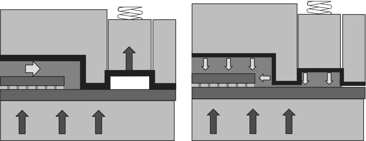
Figure 17.23 Mold tool design with overflow mechanism: (left) during clamping the ring is touching the carrier system and (right) during final pressure.
17.4.7 Mold Tool Release During Compression Molding
The solidification process of thermoset materials is dominated by an exothermic chemical reaction – the curing reaction. The curing reaction is an irreversible process that results in a cross‐linked structure of molecules. Thermoset materials are mainly used for semiconductor packaging. As known from the previous explanation, curing of thermoset materials is activated by temperature. The release from the molding tool is only possible when the molding compound achieves a certain curing stage. The cross‐linking also determines the hot hardness of the material used. As the temperature of a molding compound increases, hardness decreases, and at the glass transition temperature (Tg), a drastic change in hardness occurs. The hot hardness of a molding compound is the hardness at the molding temperature. Two different methods are used in semiconductor packaging to separate the package from the mold tool.
Separation from the mold tool can be done by ejector pins. It is mainly used for standard packages, for example, BGA, QFP, QFN, etc. The limitations are very thin and large cavities or high adhesion molding compounds like LMCs. The reason for this limitation is that the molded device has to withstand the release force and bending during ejection from the mold tool cavity.
Separation by release film is used for dedicated packages like for LED packaging, MEMS packaging, or WLP. The release film advantages are a low separation or release force even for high adhesion molding compounds like LMCs and that the process can be controlled much more easily with repeatable stability.
17.4.8 Transfer Molding vs. Compression Molding Capability
Figure 17.24 shows a comparison of design rules between transfer molding and compression molding. The design rules of compression molding are better than those for transfer molding. For example, the design rules of transfer molding are strongly related to the mold‐flow behavior of molding compound due to the long molding distances.
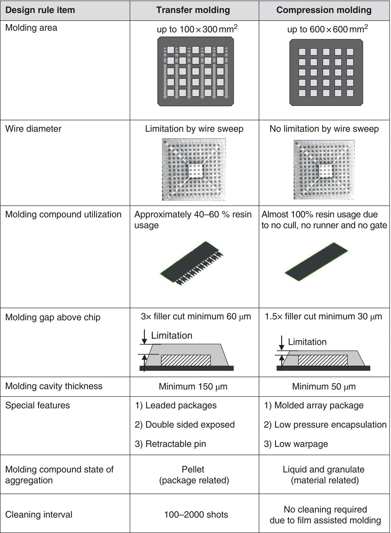
Figure 17.24 Comparison of design rules for transfer molding and compression molding.
17.5 Principle Challenges for Chip Embedding with Compression Molding
17.5.1 Cavity Filling of Large Area
The moldability of large area compression molding like for 300 mm eWLB strongly depends on the mold‐flow speed. This mold‐flow speed has to be controlled in the range of 3–7 mm s−1. If the mold‐flow speed is too low, the mold compound viscosity increases during mold filling, which leads to incomplete cavity filling. If the mold‐flow speed is too high, the risk of mold compound bleeding or internal voids can occur. Therefore, the mold‐flow speed has to be controlled very accurately and must be very slow in order to achieve optimized cavity filling especially for increasing wafer diameter or distances. The mold‐flow speed is related to the compression speed. Figure 17.25 shows a carrier system with chips, the dispensing of LMC, mold filling by compression molding, final pressure, and the molded wafer with mold carrier.
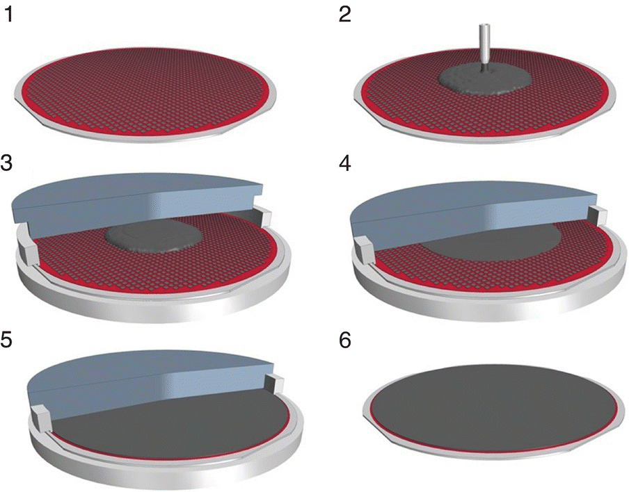
Figure 17.25 . Carrier system with chips (1), the dispensing of LMC (2), the mold filling by compression molding (3 and 4), final pressure (5), and the molded wafer with carrier system (6).
To ensure the optimized mold flow in the range of 3–7 mm s−1, a compression speed of 0.1 mm s−1 has to be applied, for example, for the 300 mm eWLB. Figure 17.26 shows the optimized compression speed depending on the diameter of the molded wafer.

Figure 17.26 The optimized compression speed (left) in relation to the diameter of the molded wafer (right).
The original toggle press could not achieve the required compression speed. Toggle presses use the so‐called toggle effect: the farther the toggle is stretched, the slower but more powerful the movement of the press becomes. The toggle press closing speed does not follow the servo motor target speed during the final closing. The reason was that the toggle mechanism focuses on the press clamp force. Figure 17.27 shows a sketch of a state‐of‐the‐art toggle press mechanism.

Figure 17.27 The toggle press mechanism was optimized on press clamping force.
The challenge was to develop a very accurate direct drive, which can control very low speeds.
17.5.2 Planarity of Large Area
The planarity of transfer molding is related to the mechanical accuracy of the mold tool. The transfer mold press has an influence on molding responses like mold flash or mold bleed and not on the dimensional accuracy of the molded part. Thus, the molding tool accuracy is a key issue for the transfer molding process. Figure 17.28 shows a sketch of a transfer mold tool concept focused on the package thickness.
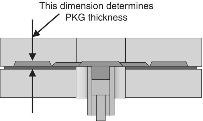
Figure 17.28 Cross‐sectional scheme of a transfer mold tool concept including the determination of package thickness.
The planarity of compression molding is related to the mechanical accuracy of the mold tool in the case of using the compression molding overflow concept. The overflow concept is pressing out the excess mold compound in a separate overflow cavity outside of the device cavity. This concept requires de‐gating after molding. The de‐gating process breaks the overflow cavity away from the device cavity. This is usually done directly after molding within automatic molding equipment. The mold tool cavity has to be spring loaded to avoid such an overflow concept and therefore the de‐gating process. The planarity of the spring‐loaded mold tool is related to the mechanical accuracy of the mold tool and the planarity of the molding press. Figure 17.29 shows the cross‐sectional scheme of a compression molding press including a mold tool and the impact of the molded part parallelism.

Figure 17.29 Compression molding cross‐sectional scheme of a parallel press (top) and insufficiently parallel press (bottom).
The challenge was to develop a very highly parallel press mechanism.
17.5.3 Dimensional Accuracy
For transfer molding, the mold tool dimension determines the mold thickness and accuracy. Compound weight deviation is absorbed by the cull thickness. The cull thickness is defined by the runner thickness and the remaining mold compound generated by the plunger stroke. Figure 17.30 shows cross‐sectional scheme of transfer mold tool including the molding compound weight deviation absorbed by the cull thickness.
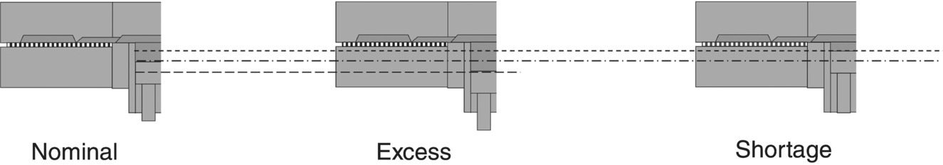
Figure 17.30 Cross‐sectional scheme of transfer mold tool and how the molding compound weight deviation is absorbed.
For compression molding the molding compound weight and the mold tool volume determine the package thickness. If the mold compound is too much, the mold thickness will be too high. If the molding compound weight is too low, the mold thickness is too thin. Figure 17.31 shows the relation between the molding compound weight and the molded part thickness for a spring‐loaded mold tool by compression molding.

Figure 17.31 Cross‐sectional scheme of the molded part thickness: target thickness (left), upper thickness deviation (middle), and lower thickness deviation (right).
The challenge was to develop a dispense method that very precisely controls the molding compound weight, even at high amounts.
17.5.4 Molded Wafer Identical to SEMI Specification
The molded wafer must be identical to the SEMI specification of a silicon wafer, because this allows the use of standard front‐end tools. This means the wafer edge should not have any irregularities like an air vent or an ejector pin. The air vents are required to bring the internal and external mold voids under control. Molding compounds with very low viscosity or with fine filler have a limitation on the air vent height due to the mold‐flow behavior. The ejector pins are required to have a proper mold release after molding compound curing. Large and thin molded areas are very critical to release due to the high mold release force and high bending properties under molding temperature. Figure 17.32 shows typical irregularities of molded parts.

Figure 17.32 Transfer molded package with typical irregularities: (left) required air vents and (right) required ejector pins.
The challenge was to develop a molding process to achieve an outer dimension identical to the SEMI specification of a silicon wafer.
17.6 Process Development Solutions for Principle Challenges
17.6.1 Cavity Filling of Large Area
The mold filling of a large area requires a very low compression closing speed down to 0.1 mm s−1. This is solved by the change of the molding press mechanism from toggle to direct‐drive ball screw. The direct‐drive ball screw press mechanism is able to achieve a very high position accuracy. This is required especially for the spring‐loaded mold tool concept. Figure 17.33 shows the construction of compression molding press with direct‐drive ball screw mechanism.
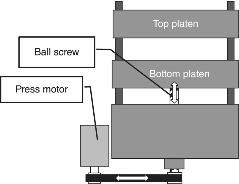
Figure 17.33 Sketch of a direct‐drive ball screw press mechanism.
17.6.2 Planarity of Large Area
The planarity of large molded areas by compression molding with spring‐loaded mold tool concept requires, a high parallelism of mold tool and mold press. To overcome this issue, a four‐corner direct‐drive ball screw press mechanism was developed instead of using the available press toggle drive. This four‐corner direct‐drive ball screw mechanism can be easily adjusted on‐site by software and enables a closed‐loop position control. Figure 17.34 shows a cross‐sectional scheme of a four‐corner direct‐drive ball screw press mechanism.

Figure 17.34 Four‐ball screw drive press mechanism that is optimized for precise press planarity during compression speed and final pressure.
17.6.3 Dimensional Accuracy
A very accurate LMC dispenser for high viscosity and for high amounts of mold compound was developed to ensure minimal thickness deviation. The dispensing accuracy is around ±0.3 g to ensure thickness control in the range of 10 μm. Due to the fact that the mold carrier system weight deviation is already more than few grams, the molding compound dispenser needs a weight‐controlled closed‐loop system. The pinch valve nozzle is very effective in terms of dispense speed improvement, especially for high viscosity LMC. Figure 17.35 shows an LMC dispenser with closed‐loop system and pinch valve nozzle.
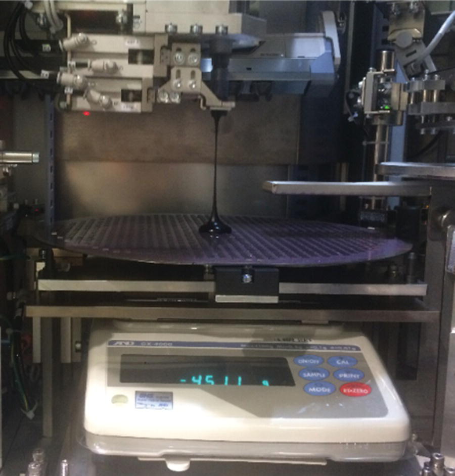
Figure 17.35 Liquid compound dispenser that is optimized for accurate dispensing and dispensing speed.
The high performance cavity vacuum was developed to eliminate incomplete fill and air vents of the molded wafers. This ensures molded wafers with identical dimension to SEMI specification. The high performance cavity vacuum will evacuate the air completely before closing. Absolute vacuum values below 20 mbar have to be achieved during compression. Figure 17.36 shows a high performance vacuum pipe system.
Figure 17.36 High performance vacuum pipe system.
The mold tool is covered completely by a release film to avoid ejector pin imprints. In addition, the release film enables a smooth releasing of the molded part from the mold tool. The release film material is usually from the resin family of ethylene tetrafluoroethylene (ETFE) or polyethylene terephthalate (PET). The important release film properties are the releasability, elongation to break, and expansion during heating up. The film‐assisted unit handles the release film automatically, and the suction into the cavity is done by a vacuum system. The mold tool is designed to ensure fully automatic wrinkle‐free processing. Figure 17.37 shows a cavity‐up mold tool covered completely with a release film.
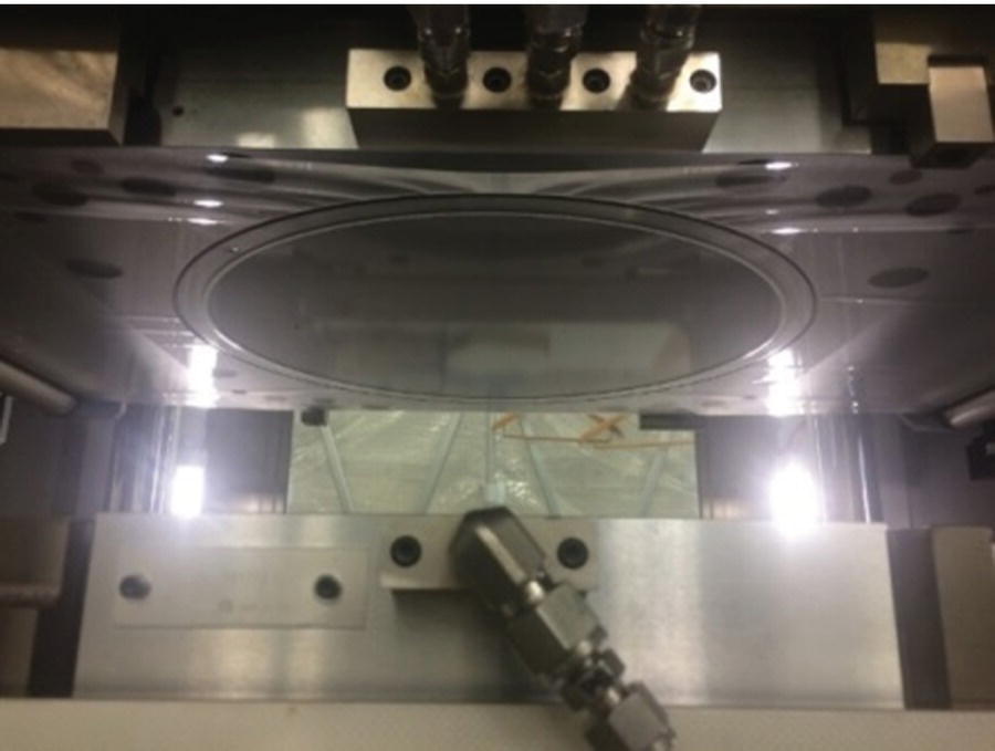
Figure 17.37 Top mold tool covered completely with release film.
17.7 Compression Molding Equipment for Chip Embedding
The compression molding for fan‐out eWLB technology required a complete new equipment development. All required challenges necessary to achieve a robust process have been addressed. In addition, the processing of bare silicon wafers (e.g. TSV, wafer bump protection, backside protection) has also been considered. The equipment consists of two newly developed compression molding presses. These presses are equipped with a four‐corner direct‐drive ball screw press mechanism to ensure the highest planarity in combination with optimized mold‐flow speed. The liquid dispensing unit is able to run very high viscosity LMCs. A granular dispensing unit can be selected as an option. The equipment has integrated PMC and post mold inspection. The handling is based on a commercial flexible robotic unit. Thus, the conversion effort is minimized. Figure 17.38 shows the fully automated compression molding system optimized for fan‐out eWLB and fan‐in WLP (bare silicon wafer).
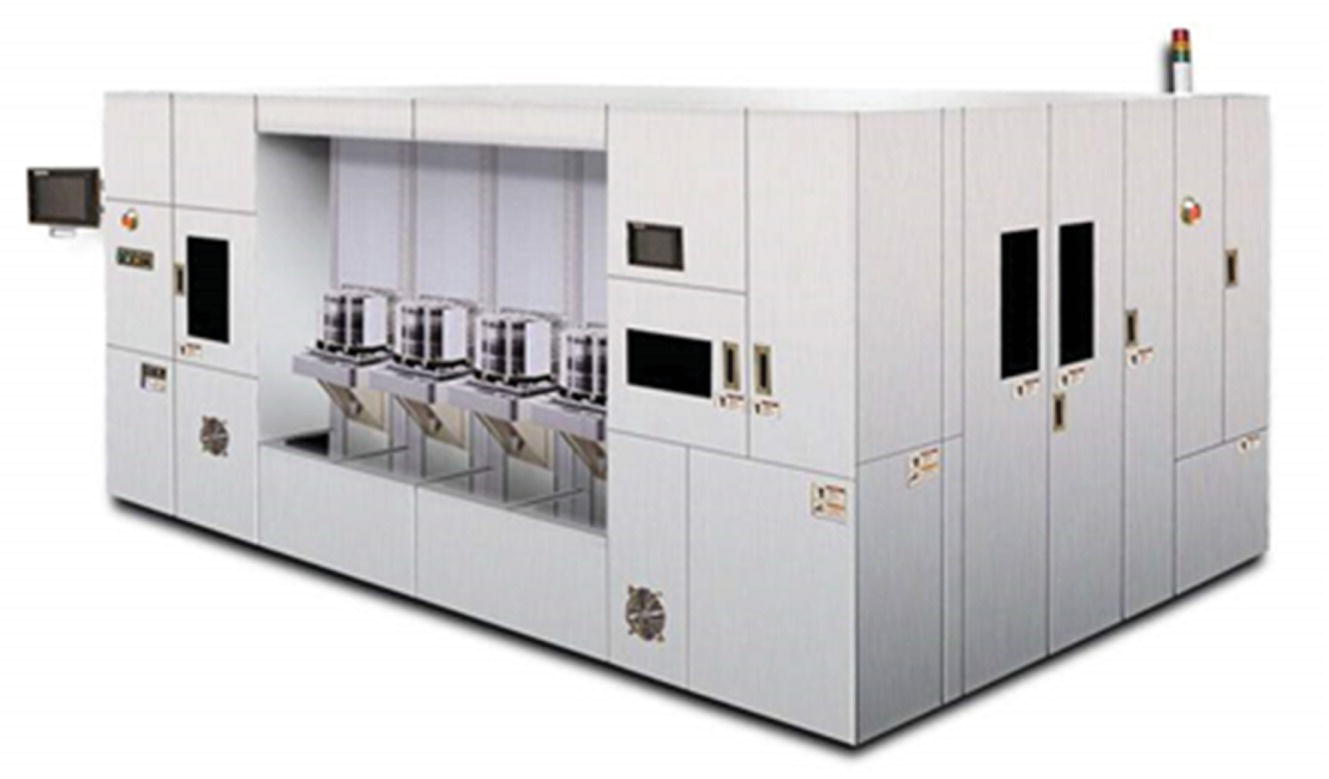
Figure 17.38 Compression molding equipment optimized for chip embedding (WCM‐300 from Apic Yamada).
This equipment, named WCM‐300, is able to process fan‐out and fan‐in wafer‐level packages with a diameter up to 300 mm (round shape). The equipment is able to operate in a clean room environment down to class 1000. Automatic magazine loading and unloading, which is required by front‐end production, can be applied. In addition, panels with a length up to 300 mm (square shape) can also be encapsulated. For larger panel dimensions, further equipment is under development.
17.8 Chip Embedding Features Achieved by Compression Molding
Applying compression molding, the results shown in Figure 17.39 for features of eWLB molded wafers with a diameter of 300 mm could be achieved.

Figure 17.39 eWLB features with corresponding results for 300 mm molded wafer technology.
The data in Figure 17.40 compare package type, total thickness variation, wafer diameter, and the overall equipment efficiency (OEE) for volume production.

Figure 17.40 Total thickness variation, wafer diameter tolerance, and overall equipment efficiency for different package types.
17.9 Conclusions and Next Steps
This chapter demonstrated the importance of compression molding for developing the fan‐out eWLB technology. The development and setup of the proper encapsulation equipment and process was of outstanding importance. The importance of the right molding material was also highlighted. The temporary rigid carrier together with the thermal release tape, the liquid mold compound, and the compression molding process were identified as the most critical parts that had to be solved in the first years of the fan‐out eWLB technology to construct the molded wafer. Special challenges that had to be solved for compression molding equipment were large area cavity filling, planarity of the large area, dimensional accuracy, and SEMI specification compliance of molded wafers.
In the future, main trends will focus on cost requirements, thinner devices, and higher system integration. System integration, i.e. the integration of more functionality into smaller volume, will be a major trend. This will include technologies like side‐by‐side, 3D integration, and integration of passives and antennas into one package. The encapsulation equipment combined with new mold material must be designed properly for this trend. One example is equipment that can position chips side‐by‐side with less than 50 μm spacing in between. Another example is preparing equipment that offers 3D stacking capabilities. For further cost reduction, the large size molding process is investigated with respect to introducing square panel format. The development of fan‐out panel‐level packaging (FO‐PLP) up to 600 mm × 600 mm or even more (see Figure 17.41) is expected to provide a significant cost reduction. In addition, material improvements are under investigation, e.g. in respect to molded wafer warpage. The industry is presently introducing new types of molding compound aggregations such as granulate (GMC) or sheet (SMC). Figure 17.41 compares front‐end‐like round wafer with square back‐end strip and PCB panels.
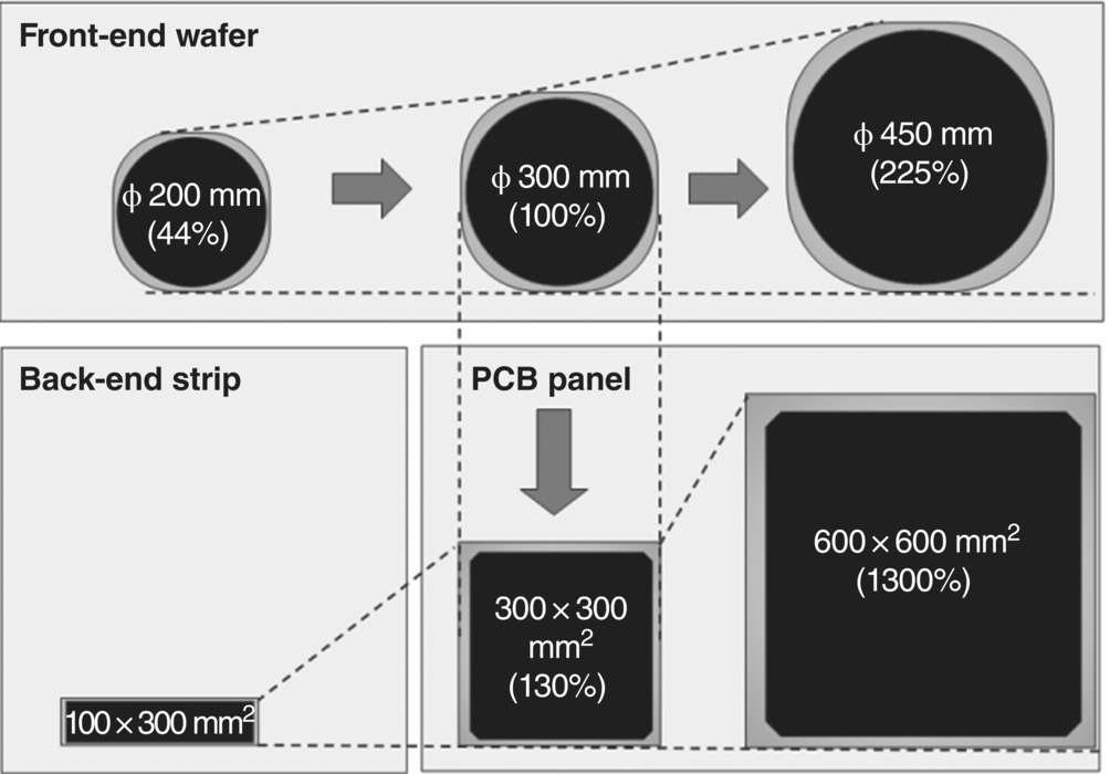
Figure 17.41 Front‐end‐like round wafers compared with square back‐end strip and PCB panels.
Acknowledgments
Infineon Technologies gratefully acknowledges the partial funding of molding processes by the project SIPHA, funded by the German BMBF (grant number 01M3177A), and by the project ESIP, funded by the ENIAC JU (grant number 120227) and the German BMBF (grant number 16 N10971).
References
- 1 Bartholomew, M. (1999). An Engineering’s Handbook of Encapsulation and Underfill Technology. Electrochemical Publications LTD ISBN 0 9011150 38 X.
- 2 Davis, B., Gramann, P., Oswald, T.A. et al. (2013). Compression Molding. Gardner Publications ISBN‐13 978‐3‐446‐22166‐6.
- 3 Brunnbauer, M., Meyer, T., Ofner, G. et al. (2008). Embedded wafer level ball grid array (eWLB). International Electronics Manufacturing Technology Conference 2008.
- 4 Fürgut, E., Beer, G., Brunnbauer, M., and Meyer, T. (2006). Taking wafer level packaging to the next Stage. SEMI Europe 2006 Advanced Packaging Conference.
- 5 Fürgut, E. (2010). eWLB reconstitution from idea to volume production. SEMI Europe 2010 Advanced Packaging Conference.
- 6 SEMI M1‐1016 (2016). Specification for polished single crystal silicon wafers; latest publication April 2016.