
1
History of Embedded and Fan‐Out Packaging Technology
Michael Töpper, Andreas Ostmann, Tanja Braun, and Klaus‐Dieter Lang
Fraunhofer IZM, Berlin, Germany
1.1 Introduction
The fabrication of microelectronic systems purely monolithically on a wafer is limited by the need for mixed technologies and redundancy. Multi‐chip modules (MCMs) provided an alternative in achieving high density interconnects (HDI) being originally developed in the 1980s for aerospace applications, where size and weight were critical requirements [1]. The core idea of MCM was therefore the reduction of the interconnection length between different electronic components like integrated circuits (ICs), passives, and others like optoelectronic components. In 1990, silicon devices of 16 mm × 16 mm were the limits of manufacturability in volume production – far from the wafer‐scale integration goals necessary for large electronic systems. Therefore, multiple ICs were needed, which resulted in a hybrid manufacturing process. Standard packaging technologies have used single packaged ICs that are mounted on the printed circuit board (PCB). The electrical signals have to travel from the IC through the package and through the PCB to the next package, limiting the high‐speed performance of the systems. This translates to long interconnection lengths between devices and a corresponding increase in propagation delay. MCM was the first approach to eliminate the package and to use a high density routing substrate instead of PCB. All ICs and also the substrates can be pretested to ensure a high yield module process.
The interconnection of the bare ICs to the MCM substrate can be done by direct chip connection using wire bonding (WB), tape‐automated bonding (TAB), or flip‐chip (FC) bonding. The basic MCM concept was first proposed by IBM in 1972 as an “active silicon chip carrier” [2]. There were three main approaches for MCM processes developed: MCM‐laminate (MCM‐L), in which a multilayer prepreg laminated board was used; high density ceramic MCM (MCM‐C), in which a multilayer co‐fired ceramic substrate was used; and thin film deposited MCM (MCM‐D), in which a thin film metal/dielectric substrate was used. The reason for building MCM‐D in the late 1980s will still sound familiar today: providing off‐the‐chip interconnect bandwidth matching the semiconductors clocking rates, decreasing power dissipation in input and output (I/O) drivers with matched impedance, and reducing the volume and size of the circuits. The difference between then and now is a major push for low fabrication costs to satisfy the consumer markets. System in packages (SiP) can therefore be viewed as an extension of an MCM. In addition, the lack of availability of known good die (KGD) for the different applications was a major hurdle to get functional MCMs with a sufficient yield. All of these types were in principle “chip‐last” technologies in which the interconnection substrate is manufactured before the chip attachment being done by FC, WB, or less used TAB. “Chip‐first” is the usage of an embedding process where the chips are placed under the interconnection layer. The chips have to be placed onto or within a base substrate prior to the fabrication of the interconnect structure that is then a direct metallurgical contact eliminating FC, WB, or TAB. With such an electrical interconnect, a reference ground plane can be deposited directly onto the chip pads, which provide a very well‐matched high frequency interconnect structure. The inductance and the capacitance are over 10 times lower compared with FC, TAB, and WB.
Therefore embedding‐type MCMs have been developed to bypass the yield issue for monolithic wafer‐scale integration. Main pioneering work was done by Wayne Johnson from Auburn University and Ray Fillion from GE Research. Johnson et al. proposed a hybrid that uses pretested ICs mounted into cavities etched in a silicon wafer [3]. A schematic of this concept is shown in Figure 1.1.

Figure 1.1 Schematic of an embedded MCM proposed by Johnson et al. [3].
Source: Reproduced with permission of IEEE.
The chips are interconnected with planar thin film process steps. An additional metallization layer is used for the interconnection to the next packaging hierarchy. The cavity is etched anisotropically into a silicon wafer using standard MEMS technology, which gives 54.74° sidewall angles. A 15 μm thin Si membrane was left to facilitate the deposition of the metal routing on the top Si surface. This membrane was removed by dry etching before chip embedding. The components are inserted from the backside and glued inside the thermally oxidized Si carrier with an adhesive (epoxy resin with 75% inorganic filler). In one of these first embedding approaches, benzocyclobutene (BCB) was deposited on top of the Si wafer containing four ICs for planarizing the surface of the substrate for the subsequent routing process. The low curing temperature is of great benefit for this embedding‐type approach due to the low thermal stability of the epoxy resin used for gap filling. After curing the BCB was structured by reactive ion etching (RIE). To correct for chip‐to‐wafer misalignment occurring during die mounting from the backside of the substrate, a computer program was written that automatically calculated a corrected pattern generator file for mask making.
An even earlier approach for embedding was patented in 1968 by Ties Siebolt Te Velde and Albert Schmitz from Philips in Eindhoven in the Netherlands called semiconductor circuit having active devices embedded in flexible sheet [4]. The invention relates to a semiconductor device comprising a layer having a number of semiconductor components that are separated from one another by an electrically insulating material and are connected together on at least one side of the layer by mutually separated conductors that are located at least partly on the insulating material and adjoin surface parts of the components that are free from the insulating material. Pictures from the patent are shown in Figure 1.2.
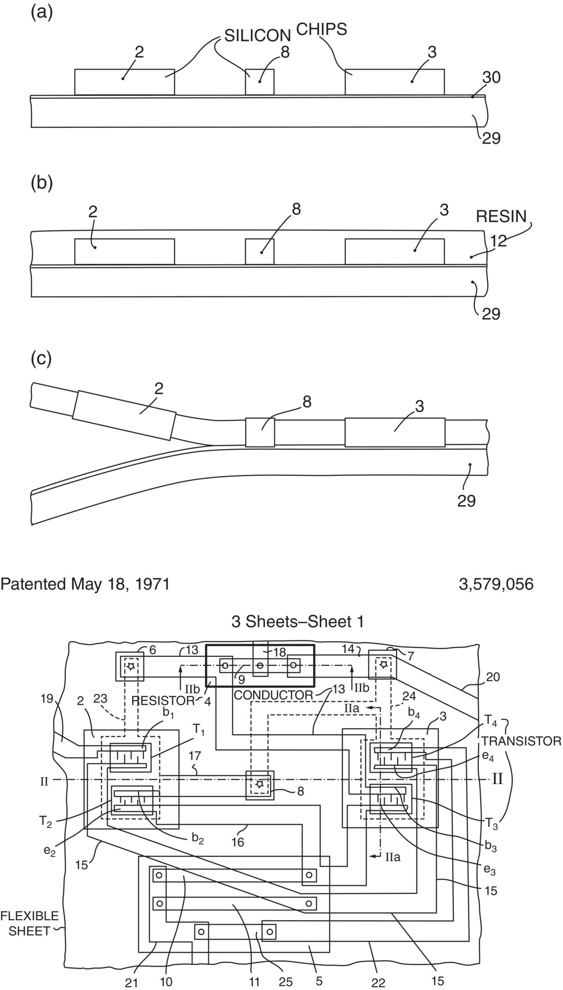
Figure 1.2 Pictures from US Patent no. 3,579,056.
The components were glued on a temporary support substrate preferable a flex (a). A layer of resin (polyurethane, for example) was then provided between and across the components (b). The temporary adhesive was dissolved to remove the embedded substrate (c). At that time, the focus for the semiconductor components was on diodes, transistors, resistors, and capacitors. Even an extensive search in the literature has not disclosed further information on this approach. It is not clear whether this technique has been further published or presented.
On the following several pages, early embedding technology developments will be summarized and grouped together in two categories: the first being more influenced by thin film technology used for the MCM‐D and the other more laminate based. There are certainly more examples being developed in the last 30 years. Unfortunately for some technologies, only limited details have been published. For sure, some technologies that also have a longer history like extended wafer ball grid array (eWLB) from Infineon or redistributed chip packaging (RCP) from Freescale are discussed in separate chapters in this book.
1.2 First Embedding Technologies Based on MCM‐D Concepts
1.2.1 GE High Density Interconnect
General Electric (GE) was a pioneer in the embedding technology [5–7]. In the mid‐1980s, GE was the first company to commercialize the embedding concept called the GE HDI technology to address harsh military environments and/or high performance computing. The HDI MCM technology embeds bare chips into a substrate under a polymer/metal multilayer that interconnects the components directly without the need for wire bonds, TAB, or solder bumps (Figure 1.3).
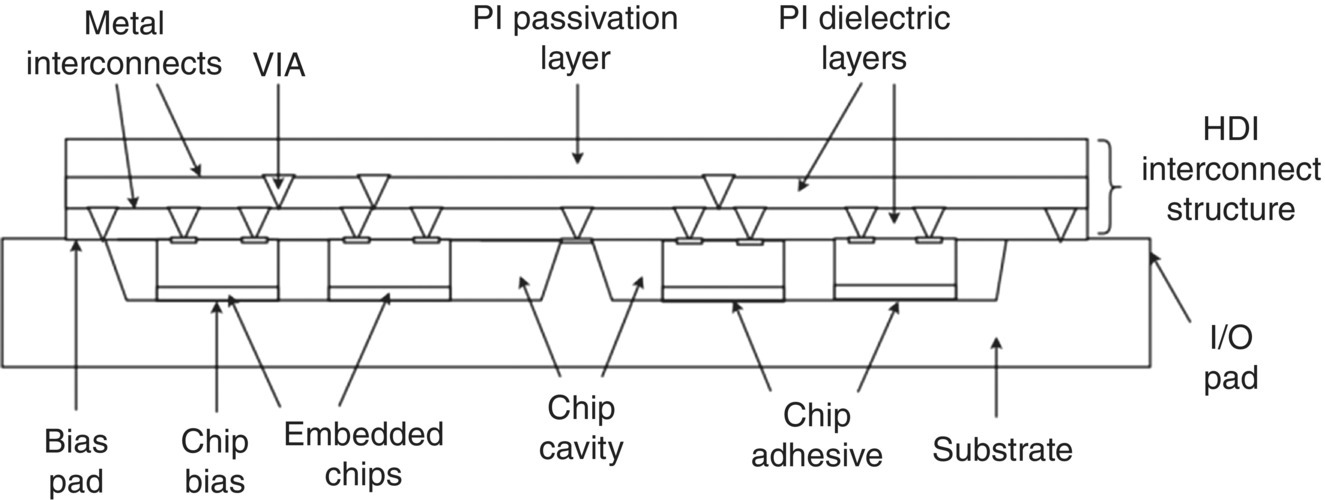
Figure 1.3 Principle of the GE HDI embedding technology.
GE used Kapton polyimide (PI) films for the dielectric isolation, and laser technology was used for the via formation. Texas Instruments had installed the HDI technology into a merchant market MCM foundry in Dallas. The process flow of the GE HDI embedding technology is shown in Figure 1.4.

Figure 1.4 GE HDI embedding process flow [8].
Source: Reproduced with permission of John Wiley & Sons.
The basis of this technology is the placement of chips of various types nearly edge to edge in cavities milled into a ceramic substrate [6]. A multilayer thin film interconnection structure is built on top of the chips and the ceramic substrate starting with a glued PI film on top of the embedded chips. The overlay film was bonded in a high temperature press under vacuum and bridges the gaps between chips and the ceramic frame. Laser ablation (5 W ultraviolet [UV] laser at 351 nm) was used to open the bond pads of the ICs. The laser system was able to accommodate the 25–75 μm misplacement of the embedded chips. An optical microscope was attached to the laser system and was used to measure the actual chip positions including rotations. A software then adapted the via locations and interconnect (metal trace) artwork to conform to each unique substrate. Vias were formed by the laser with 25 μm width on the top and 12 μm at the bottom. In addition, the long focal depth of up to 200 μm of the laser could easily accommodate the 50 μm nonplanarity inherent with the embedded chip structure due to tolerances on the cavity depth, die thickness, and die attach bond line thickness. A standard PI/Cu thin film multilayer process of spin‐coating PI and a fully subtractive metal process by sputtering (Ti/Cu) and electroplating Cu (4 μm thick) with a subsequent sputtered Ti layer to prevent Cu migration were used. The photoresist for the metal etching process was also structured by laser scanning using the data from the optical inspection. Already in 1990, this technology had been applied to more than 20 different circuits. These included radiation test structures, daisy chain test cells, 6‐ and 9‐chip digital signal processing (DSP) modules, 25 chip random‐access memory (RAM) modules, 36‐chip multiprocessor circuits, analog functions, 16‐ and 52‐chip image processing circuits, a 13‐chip data processor circuit, and power modules like DC‐to‐DC power converter [5, 9].
A further development project started at GE in the early 1990s to lower the cost of the first HDI technology. Different possibilities were discussed, including a modified process that utilizes an FR‐4 PCB as the substrate, eliminating the milling step for the ceramic substrate. FR‐4 has been one of the standard flame‐retardant (FR) (class 4) PCB materials since the 1970s. Most promising was the plastic encapsulated HDI MCM [9]. The process flow is shown in Figure 1.5.
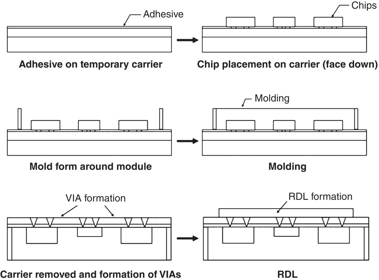
Figure 1.5 GE plastic encapsulated HDI process flow.
The bare chips or passives were mounted facedown onto an adhesive‐coated polymer film. An industry standard epoxy blend encapsulant was selected with a coefficient of thermal expansion (CTE) of 6 ppm K−1 closely matched to silicon by a 70% solid content. The material was 100% compatible with the other HDI multilayer materials. A mold form was then placed around the chips, and a molding material was deposited into the mold form. The substrate was formed out of the combination of components and cured polymer. A polymer/metal multilayer was then deposited on the flipped embedded substrate to interconnect the different embedded components. A major advantage of the plastic encapsulated process compared with the ceramic approach was the much higher planarity of the surfaces, including filling of all open gaps. The issue of high power dissipation of the chips could be eliminated by using thermal plugs made out of a high thermal conductance material such as AlN, copper, or a composite structure, which were attached directly to the exposed backside of the embedded module. Also, through package vias were under discussion in 1994 by embedding metal pin grids into the mold. The first modules were demonstrated on 150 mm square size in 1994 with the outlook on 12–18 in. in the future [9]. One commercial product was a phased array radar application [10]. EPIC was founded in 1994 by former GE employees. They developed a technology called “EPIC Chip First” and started production in 1996 primarily for government systems in low volume.
1.2.2 Fraunhofer IZM/TU Berlin
The chip‐first approach developed at the Fraunhofer IZM/TU Berlin since the early 1990s was different than the HDI from GE due to the aligned bonding of the components to the ceramic opening that opened the possibility of using masks for the later lithography [11, 12]. The process flow is shown in Figure 1.6.

Figure 1.6 Process steps of the embedding process: laser cutting of the ceramic, chip placement using optical alignment, and filling of the gap between embedded components and substrate by an epoxy.
The chips were inserted into windows of ceramic (Al2O3, AlN) or silicon substrates. The windows for the active and passive components were laser cut by computer‐controlled Nd:YAG laser equipment. The windows were around 100 μm larger than the components in the x/y‐direction. A PI film with an adhesive was then laminated on the frontside of the substrate. The substrates were fixed to a glass mask. Using an optical alignment system, the components were inserted face‐up into the windows. They were fixed in their position by the tacky PI film. The accuracy in x/y‐direction of the positioning was better than 5 μm. Different from the HDI approach from GE, a mask process already used in high production for bumping and redistribution could be used to open the vias above the chip pads and to define the interconnection lines that contact the chips. No laser processing was required. The substrate was turned upside down, and a filled epoxy was dispensed into the gap between the substrate and the components. After curing the epoxy and lapping the back of the substrate, the auxiliary film was removed. The surface was cleaned with a short plasma step. The highly planar embedded substrate was now ready for the thin film wiring, starting with a layer of photosensitive polymer. Therefore, spin‐on polymers rather than dry films could be used, which broadens the range of materials being used for the routing. Especially, spin‐on low‐k polymers were needed for RF applications [13]. A low‐k polymer is a material with a dielectric constant smaller than that of silicon dioxide, enabling faster switching speeds and lower heat dissipation by reducing parasitic capacitance. An example of an embedded SRAM is shown in Figure 1.7.

Figure 1.7 Embedded SRAM in AlN (SEM) and with the first photosensitive BCB and copper layer (SEM; BCB is etched for visualization).
To demonstrate the compatibility of the embedding technology, an MCM with eight SRAMs and four surface‐mount device (SMD) capacitors (220 nF, size 1210, thickness 600 μm) was fabricated using AlN as the embedding substrate. The components were interconnected by a four‐layer metallization. The dielectric polymer was mostly photosensitive BCB (10 μm thick) due to the low curing temperature of below 250 °C. A higher curing temperature would degrade the epoxy‐filled gap. The copper lines were 30 μm wide and 5 μm thick. Figure 1.8 shows the first three metal layers over the chip, the metallization over the gap, and a cross section through the four‐layer metallization interconnecting the embedded components.

Figure 1.8 Multilayer metallization (Cu/BCB) over the SRAM (video print). Metallization over the gap (BCB was etched for SEM); cross section of the four‐layer metallization interconnecting the embedded components.
On the embedding substrate, the redistribution is no longer limited to a fan‐in, but the rerouted pattern and the final package can exceed the die size, enabling fan‐out packaging structures [14]. Embedding in a carrier substrate is not restricted to only one die size, but different die from different technologies can be inserted at the same time. When a fan‐out redistribution is deposited, the die itself will be completely encapsulated by ceramic and gap filler material. So the die is no longer exposed to mechanical damage risk by pick and place handling. Examples of such fan‐out single chip packages using embedding technology are shown in Figure 1.9.
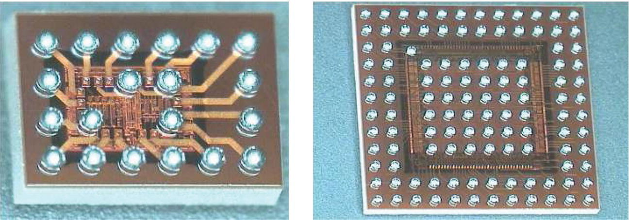
Figure 1.9 Small die with fan‐out BGA pitch of 0.5 mm (left) and large die embedded with 0.4 mm BGA pitch with a package size of 9.6 mm × 9.6 mm (right).
To accommodate 300 μm solder balls, the under‐bump metallurgy (UBM) dimensions were chosen as 250 μm in diameter and with a thickness of 5–10 μm. The Ni surface is protected against oxidation by a 100 nm chemical Au deposition before placement of the solder balls. Crosscuts of such fan‐out packages are shown in Figure 1.10.

Figure 1.10 Crosscut of fan‐out embedding die with a completely encapsulated die and revealing package details above embedding interface (Cu routing, Ni‐UBM, PbSn solder ball).
This planar integration of hybrid technique was also employed to achieve a stackable MCM. Vertical integrating systems of such high complexity with the shortest chip‐to‐chip interconnects require numerous electrical feedthroughs in the MCM substrate and vertical interconnects between mating submodules. For that purpose, prefabricated miniaturized contacting elements (thin film Cu/polymer routing) that provide the required high number of vertical electric connections were embedded in the embedded substrate materials [15]. The invention allowed vertical electric connections to achieve the high quality of usual horizontal thin film routing (Figure 1.11).
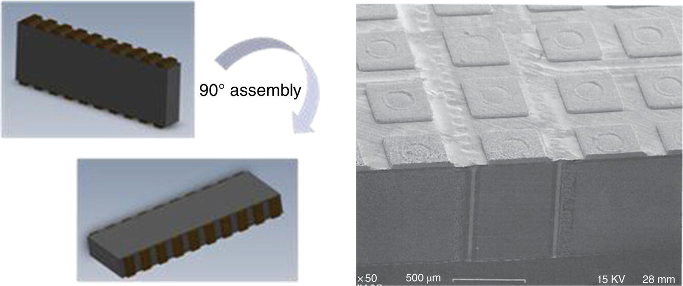
Figure 1.11 Vertical interconnect element (VIE) (manufacturing, sawing, 90° turning) and SEM of such a VIE (30 μm × 50 μm).
The contacting elements had been embedded in the substrate materials by the same planar junction technique. Such separately pretested submodules with a dual‐sided bump‐array metallization had been stacked to realize the shortest interconnects between a large number of ICs [16]. To accomplish repair or system changes, removable elastomeric connectors were sandwiched between mating substrates and kept under moderate pressure. The process is shown in Figure 1.12. Compared to common 2D integration, reduced signal delay and reduced parasitic effects like resistance, capacitance, cross talk, and inductance resulted in better electrical performance. In 1997 and 1998, results indicated that the impact of small variations in geometry caused by the technological embedding process on the line parameters meets the practical requirements in terms of signal transmission. Microstrip structures for the wiring on the embedded substrate using BCB as dielectric are well suited for high frequency applications in the 20–30 GHz range [17, 18]. Small pretestable subunits, with a moderate number of integrated components and their easy exchange in the stack, should lead to a high system yield.
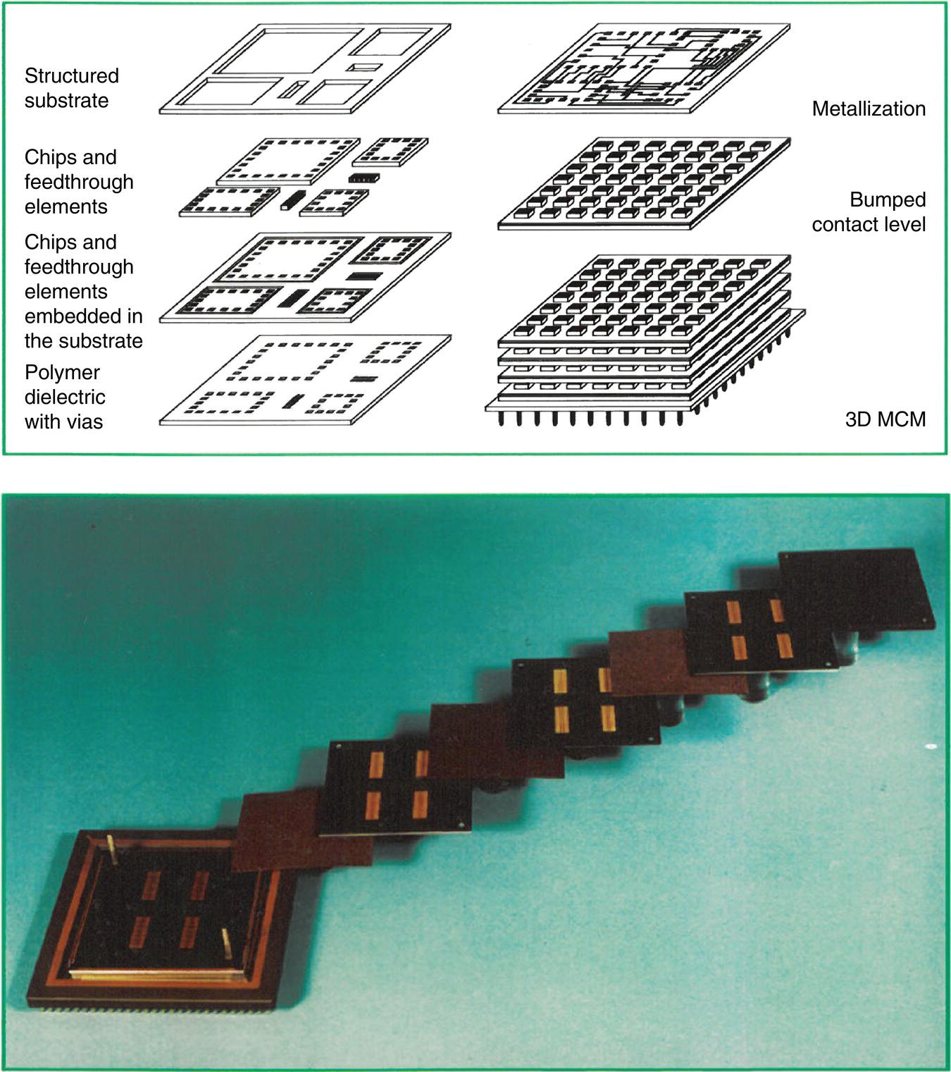
Figure 1.12 Schematic of the 3D concept of the embedding technology and view of submodules and elastomeric conductive interlayers mounted on a PGA [16].
This embedding technology is also an excellent solution for one of the most crucial issues in power module designs, which is the assembly of large structural components – the circuit substrate and the heat sink – together. In addition, the thermal expansion mismatch between the components could be absorbed by the embedding process. A process modification was done for such power modules that involved the embedding of high power dissipating ICs in a substrate that was thinner than the chips and mechanical planarization of the substrate backside [19]. The process flow is shown in Figure 1.13. A homogeneous low thermal resistivity contact to the cooling body could be accomplished simultaneously for all embedded components due to the planar backside finish.
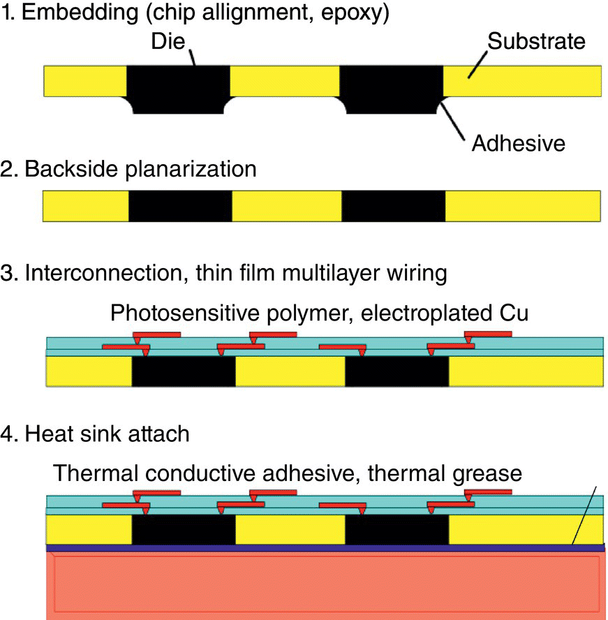
Figure 1.13 Process flow of the planar embedding technology for power modules: (1) embedding with epoxy, (2) backside planarizing, (3) thin film multilayer wiring, and (4) low thermal resistance heat sink attach.
Using this technology, high power MCMs were fabricated with a junction to ambient thermal resistance below 0.6 Kcm W−1 normalized to the chip area. This was achieved by embedding the chips into the AlN substrate, planarizing by lapping/grinding the module backside, and bonding to high performance microchannel heat sinks with high conductivity adhesive. Values down to 1.25 Kcm W−1 had been obtained by use of thermal grease materials. The low thermal interface resistance had been obtained simultaneously for all embedded dies. AlN microchannel heat sinks were fabricated by laser machining. Thermal resistances of the heat sinks below 0.6 Kcm W−1 (0.03 K W−1) were obtained at a pressure drop below 1 bar and a water flow of 60 l h−1. Figure 1.14 shows the thermal test of MCM with a size of 2 in. × 2 in. with six thermal test chips capable of a power dissipation up to 1000 W in a volume of 50 mm × 50 mm × 3 mm.

Figure 1.14 Thermal test of MCM with a size of 2 in. × 2 in. with six embedded thermal test chips and assembled on a heat sink.
A development of a fully Si‐based embedded module was done in the Smart Power project from 2011 to 2016 funded by the EU. The goal of the project was to carry out the packaging and thermal management development required to achieve the efficient and cost‐effective implementation of SiC‐ and GaN‐based power modules into industrial power inverters and RF transmitter systems, respectively. One packaging approach was the embedding process of a GaN high power amplifier (HPA) with its GaN driver together with all passive components into an Si cavity [20]. A schematic of the embedding approach is shown in Figure 1.15.

Figure 1.15 Simplified schematic of the embedding of an Si RF power module.
Two thermal sensors were added for temperature monitoring: one based on a surface acoustic wave (SAW) chip and the other one lithographically formed directly on the silicon surface package. Basically, the process flow started with a deep reactive ion etching (DRIE) step to create the cavities where the components were later assembled. A ground layer was formed on the silicon substrate by sputtering and electroplating, lining the complete module. AuSn solder pads were structured and deposited by 3D lithography and electroplating into the cavities. Wafer‐level assembly was done by pick and place of the single devices from dicing tape and/or waffle packs. The assembled parts were reflowed and soldered inside the cavities. The wafer was completely filled with a polymer layer, closing the gap between components and cavity edges. Pictures of the module at different stages are shown in Figure 1.16.

Figure 1.16 Video print of the topside of the embedded components and after multilayer RDL.
By means of successive lithography steps, a redistribution layer (RDL) layer for building component interconnections and a shield layer were deposited in a strip line configuration. Low‐k BCB polymer layers were used to isolate them. Photo‐structuring in combination with excimer laser structuring the vias into the polymer was done to feed the contacts. A final passivation layer was applied and structured above the shield, and a UBM was deposited on top. Finally, a wafer‐level ball mount process was used to mount 20 000 solder balls on the wafer before being diced, resulting in a hybrid component with ball grid array (BGA) connection pads, fully compatible with SMD assembly as shown in Figure 1.17.

Figure 1.17 Crosscut through the embedded module with the multilayer wiring: on the left picture the embedded GaN components are seen, and on the right picture the interconnect of the RDL to the HPA Au Pad is shown in detail.
The wafer‐level processing was carried out on a 200 mm wafer. Therefore, packaged modules containing 11 active and passive components in a 10.5 mm × 9.0 mm area allowed the fabrication of up to 260 highly integrated modules per wafer.
1.2.3 Thin Chip Integration
The extreme developments in thinning techniques opened the possibility to further develop the embedding technology in 1999. The basic idea of the concept called thin chip integration (TCI) was to embed ultrathin die directly into the RDL [21]. For this technology, a base chip at wafer level was used as an active substrate for smaller and thinner die. Active components could be mounted in FC fashion on the base IC wafer using solder interconnects. To avoid the need for FC bonding, the TCI concept had been developed [22]. Key to this approach was the use of extremely thin ICs (down to 20 μm thickness and less), which were incorporated into the RDL (Figure 1.18).
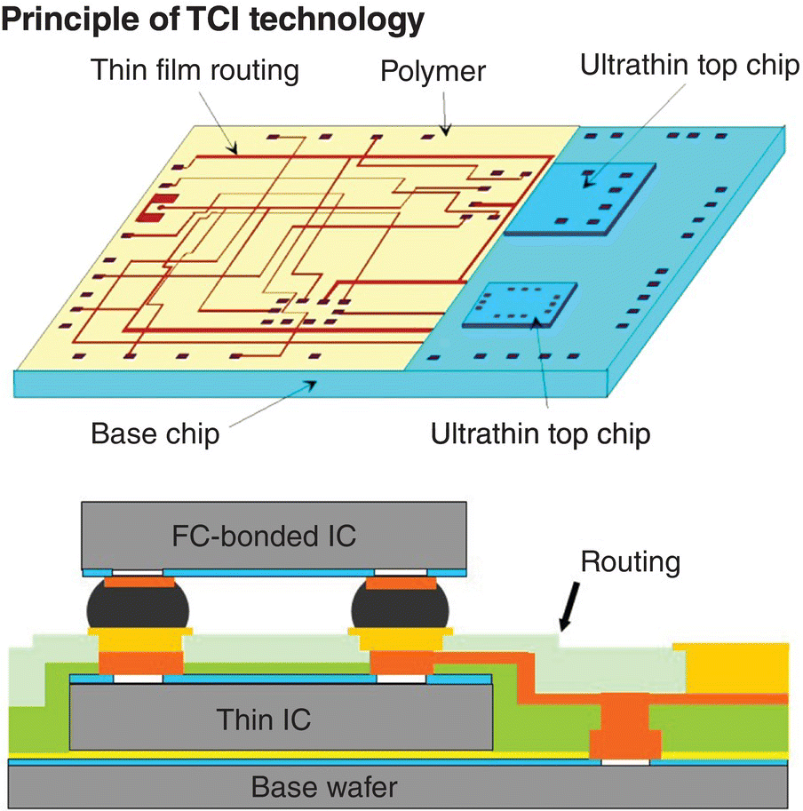
Figure 1.18 Principle of TCI.
The process flow for TCI modules began with the bottom wafer carrying large base chips. The completely processed device wafers for the top IC had to be mounted on a carrier substrate by a reversible adhesive bond and undergo a backside thinning process until the thinned wafers were 20–40 μm thick. The thinned top wafer and its carrier substrate were singulated, thus producing thin chips that could be handled by its carrier chip, just like any other standard die. A Cu routing layer was deposited on the base wafer. A combination of sputtered TiW/Cu and electroplated Cu was used, which had a low electrical resistivity. The Cu could be over 10 μm thick. The additional integration of passive components such as resistors (R), inductors (L), or capacitors (C) was possible. The bottom wafer was coated with a thin photosensitive BCB layer film, and the thinned top chips were placed and mounted into this adhesive layer. Next, the photosensitive thin film polymers like BCB, polybenzobisoxazole (PBO), and PI were deposited onto the surface to planarize the topography of the mounted thin chips. A high degree of planarization (DOP) was very important for this first polymer layer to overcome the height difference between the surface of the bottom chip and the thinned chips. A final metallization of Cu/Ni/Au for the FC bonding was deposited on the base wafer carrying the embedded ICs.
In a three‐chip test vehicle for TCI, the ICs for the process were thinned to around 20 μm. In Figure 1.19, a picture and cross section of the TCI are shown [23].

Figure 1.19 TCI test vehicle after flip‐chip attach on wafer level and crosscut through the three‐chip stack.
In a public‐funded project called RESTLES (Reliable System Level Integration of Stacked Chips on MEMS), the TCI had been also tested using MEMS and ASIC for a speed sensor [24]. Here a MEMS wafer was used as the base wafer. Within this project, the TCI technology was therefore named SCOM (stacked chip on MEMS) [25]. The base wafers contained inertial sensors. The wafer with the smaller‐sized chips (e.g. ASIC chips) was thinned down on wafer level to a thickness of 10–40 μm and diced. These thinned chips were glued onto the base wafer with a BCB layer. The polymer had been deposited and structured before gluing the next chip on top. After placement of the thinned chips, the wafer was again coated with BCB to embed the chips. The next step was the buildup of metal routing using a semi‐additive Cu process together with further thin film polymer layer with higher toughness like PI or PBO for stress compensation between solder balls and the later soldering process on an organic board. Then a UBM was added using electroplating. Finally, the solder ball application was done by ball drop. The wafer was then diced, and the full ASIC‐MEMS package could be FC‐assembled onto a PCB (Figure 1.20) [26, 27].
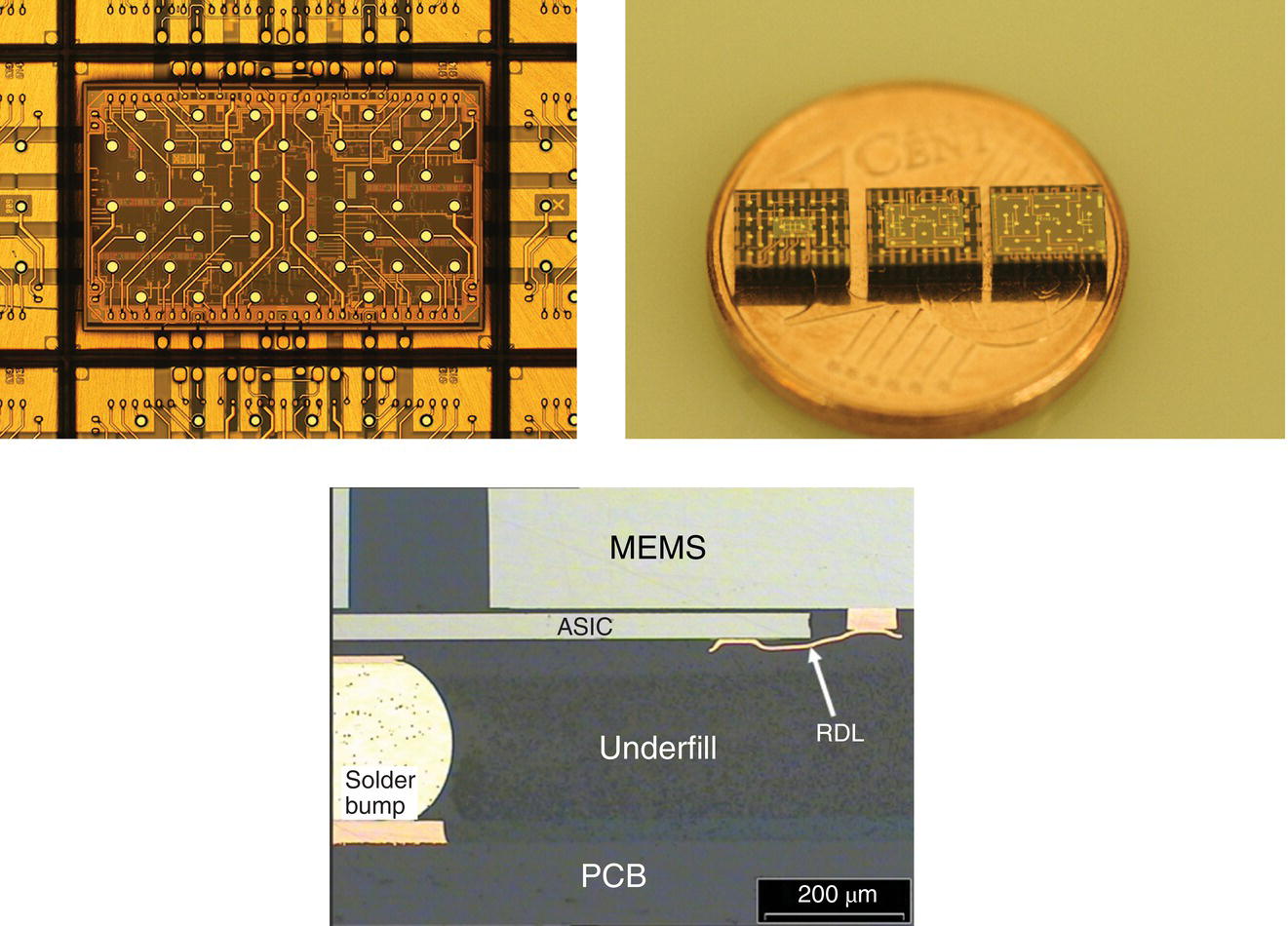
Figure 1.20 TCI for MEMS: RDL on the embedded ASIC, fully processed SiPs, crosscut.
Even after 2000 thermal cycles (−40 to +150 °C), no defect had been detected in the TCI stack for this automotive application.
A TCI test vehicle for packaging of light‐emitting diodes (LEDs) was proven and published in 2013 [28]. The LED dies were fabricated by OSRAM Opto Semiconductors GmbH. The thickness of the epi‐layer was 6 μm. On both sides, there was a thick gold metallization of 1–2 μm. The metallization was directly deposited onto the epi‐layer. The growth substrate had been removed. Due to the very low thickness of the die, the embedding technology was perfectly applicable. The intention of the concept was to glue the LEDs with their optical active side to a glass support. Therefore photosensitive BCB had been used. Copper lines were plated on a glass wafer. To contact the corner pad, an Sn layer was deposited. Copper pillars were used to bring the corner pad contact to the same level as the LED backside contact. The LEDs were glued on a first BCB layer. Afterward, the whole wafer was reflowed to establish the solder bond. A second BCB layer was used to embed the LEDs. Copper and Sn were plated to bond the modules to a substrate. Finally each module with four LEDs was soldered to the ceramic substrate. Figure 1.21 shows a cross section after this step and a complete module operated at 7 mA. The solder joint from the copper line to the corner pad can be seen.
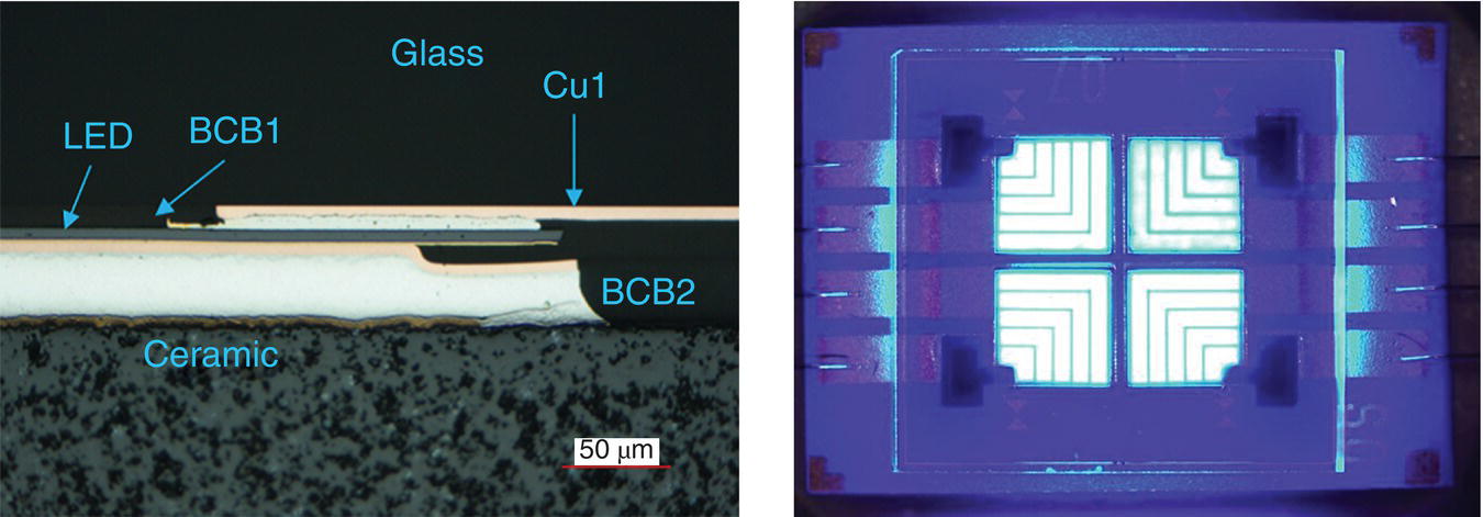
Figure 1.21 Embedded LED: cross section, complete module on AlN substrate and module operated at 7 mA.
To test and operate the modules easily, the ceramic substrates had been glued to an insulated metal substrate board. A die attach adhesive with a thermal conductivity of 60 W mK−1 was used. The pads were connected by gold WB. Using this technology, 3200 LED die could be placed on a 150 mm wafer, which is equivalent to 800 modules with 4 LEDs.
1.2.4 Irvine Sensors
Irvine Sensors was founded in 1980 to develop high density 3D stacking technologies mainly for US defense and space programs. They started a cooperation with IBM for 3D stacking using the NEO‐wafer fabrication [29]. Au wire bonds were deposited on chip pads to form Au bonds for the next interconnection level. The chips were then placed in a molding frame and were encapsulated by molding compound, forming the so‐called NEO‐wafer. The Au balls protruded through the mold. The RDL was formed on top of the surface using PI and Au. Finally, the NEO‐wafer was thinned (around 100 μm) to open the backside of the die surface (see Figure 1.22).

Figure 1.22 Principle and example of the NEO‐wafer concept from Irvine Sensors.
This process was designed to realize 3D stacking of such NEO‐wafers that could be created from individual and heterogeneous chips (see Figure 1.23). Blank silicon was added to open areas on layers where smaller dies were used to enhance thermal conduction between layers if needed. After the lithography and metallization process, the NEO‐wafers were diced into identical sizes that contained each layer to be stacked.
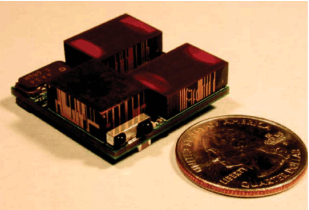
Figure 1.23 3D stacking using the NEO‐wafer principle.
Mature stacking technology and tools were used to stack many layers and interconnect layers.
1.2.5 3D Plus
The French company 3D Plus started in 1996 as a spin‐off from Thales (France). With more than 70 000 modules in space, 3D Plus is the largest space‐qualified catalog products and custom SiP manufacturer in Europe. Since 2011, the company is part of HEICO. They have developed the high performance package‐in‐package (HiPPiP) technology – a modified package on package (PoP) [30]. The fundamental process step is the placement of plastic packages on an adhesive foil that is overmolded and thinned. After the deposition of the RDL in order to build a fan‐out from the terminals of the packages, the layers with molded packages are stacked, and the vertical interconnection is performed using the laser‐assisted metallization process from 3D Plus. This process was further enhanced for unpackaged components (typical thickness 100 μm) being patented as WDoD (Wirefree Die‐on‐Die) technology [30]. The process starts with the deposition of an adhesive on silicon or glass carrier (see Figure 1.24).

Figure 1.24 First part of the process flow of the Wirefree Die‐on‐Die (WDoD) technology.
Die are assembled on the adhesive with accuracy better than ±5 μm. Compression molding of an epoxy resin over components and grinding (optional) is done as the next step. An RDL is deposited over the embedded components after de‐taping (see Figure 1.25).
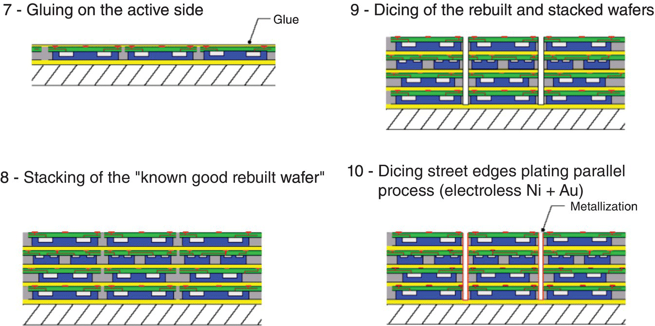
Figure 1.25 Second part of the process flow of the Wirefree Die‐on‐Die (WDoD) technology.
Nonconductive glue is used for stacking the tested layers. Dicing of the rebuilt and stacked layers is done as the next step, and the sidewalls are metallized. Finally, direct laser patterning with a pitch of 100 μm is performed for the electrical contact between the layers.
1.2.6 Casio and CMK
The embedding technology developed by Casio and CMK was called embedded wafer‐level packaging (EWLP) [10, 31]. The process starts with standard redistributed wafer‐level packages (WLPs) placed on a carrier (see Figure 1.26).

Figure 1.26 Process flow of EWLP.
The WLPs have Cu pillars on top that are embedded by a laminate using a hot press process. A laser process is used to open the Cu pillars. A combination of electroless Cu and electroplated copper is used for the interconnection of the die. The modules are bumped after the deposition of a solder mask. One product was a miniaturized wristwatch containing a speed meter for runners.
1.2.7 Panel‐Level Molding
The massive trend for higher productivity and lower cost has pushed the embedding process further to a chip‐first approach using molding on large panels. At Fraunhofer IZM in Berlin, one of the first panel molding machines at 24 in. × 18 in. has been installed [32]. An example of such a panel is shown in Figure 1.27.
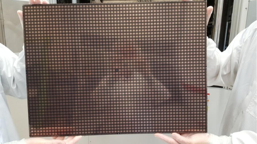
Figure 1.27 Example of a 24 in. × 18 in. fully populated molded panel with embedded die.
The large panel size equals a typical PCB format and is selected to achieve process compatibility with cost‐efficient PCB processes. Such a “mold‐first” process starts with die and fiducial assembly on an intermediate carrier followed by overmolding and debonding of the molded wafer/panel from the carrier. Compression molding is done at constant temperature, typically in the range of 120–130 °C and under pressure and vacuum to achieve a homogeneous encapsulation without voiding or air entrapments. The molding materials are liquid, granular, or sheet compounds [33]. One key process step for homogeneous large area embedding is material application before compression molding. Where sheet compounds already deliver a uniform material layer, the application of liquid and granular compound must be optimized and adapted for a homogeneous distribution without flow marks, knit lines, and incomplete fills. Hence, dispense patterns of liquid and granular molding compounds are studied to achieve high yield and reliable mold embedding. In addition, applicable thickness ranges, total thickness variation, voids, and warpage are investigated for the different material types. From the processing point of view, the liquid materials are dispensed in the middle of the cavity and flow during closing and compression of the tooling to fill the entire cavity. However, a granular compound is distributed nearly homogeneously all over the cavity. The compound melts and the droplets have to fuse during closing and compression of the tool. Sheet compound offers easy application options, as the sheet has to be only applied on the panel and melts, flows around the die, and cures during compression molding. The molding process is shown in Figure 1.28.

Figure 1.28 Process flow of the panel‐level molding process using granular molding compounds at Fraunhofer IZM.
A glass or metal carrier with the assembled die is shown in (a) of Figure 1.28. Granular molding compound is distributed over the panel, as shown in (b)–(d). The panel is molded using heat and pressure (e). After this molding process, the panel is ready for the RDL process being based on thin film or PCB technology (f). The process has been also proven for multi‐project runs [34].
1.3 First Embedding Technologies Based on Organic Laminates and Flex
1.3.1 GE Chip‐on‐Flex
A further modification of the HDI technology was done by GE using prefabricated flex circuits with direct attachment of the bare chips [35, 36]. The principle is shown in Figure 1.29.
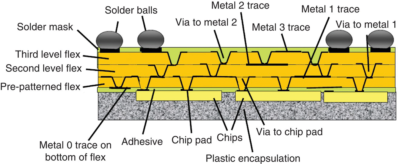
Figure 1.29 Principle of the Chip‐on‐Flex concept.
The chips were also electrically connected to the interconnect flex by forming vias through the flex directly to the chip pads with a laser, metallization of the vias and top surface, and patterning of the metal and then followed by a transfer molding process (see Figure 1.30).

Figure 1.30 GE Chip‐on‐Flex process flow.
An example of a power converter is shown in Figure 1.31.
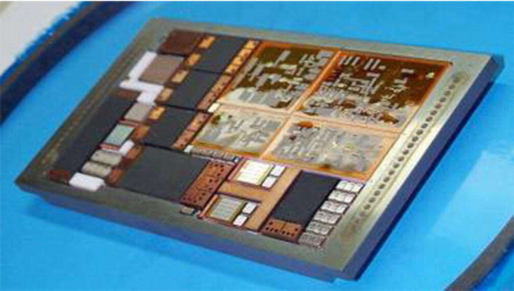
Figure 1.31 GE HDI technology: 100 W point of load power converter module.
In some publications, the name MCM‐F (Multichip‐on‐Flex) had been used for this technology. Such a multilayer structure could be thinned down to less than 100 μm, including the Si thickness of around 50 μm, using standard wafer grinders. In addition the backside of the chips can be opened to attach cooling elements or a backside metallization.
1.4 Helsinki University of Technology and Imbera Electronics Embedded Chips
Helsinki University of Technology started in 1997 a study on the solderless interconnection and packaging technique based on embedding for active components motivated by the decreasing interconnection pitch of the die [37]. Imbera Electronics, a spin‐off from the university, further developed this technology. Several generations of their integrated module board (IMB) technology to embed discrete electronic components with low‐ to mid‐range numbers of I/Os (2–350 I/Os) inside a low cost organic PCB have been demonstrated since 2002 [38]. The technology had been proven for CMOS, GaAs, and several discrete C and R components. One focus of the development was the use of standard, widely available materials and processes. In the first IMB manufacturing processes (IMB‐A and IMB‐B), the components were embedded inside a PCB core layer, and the interconnections between the IC and the copper conductor were done using buildup layers and chemically plated micro‐vias (see Figure 1.32).
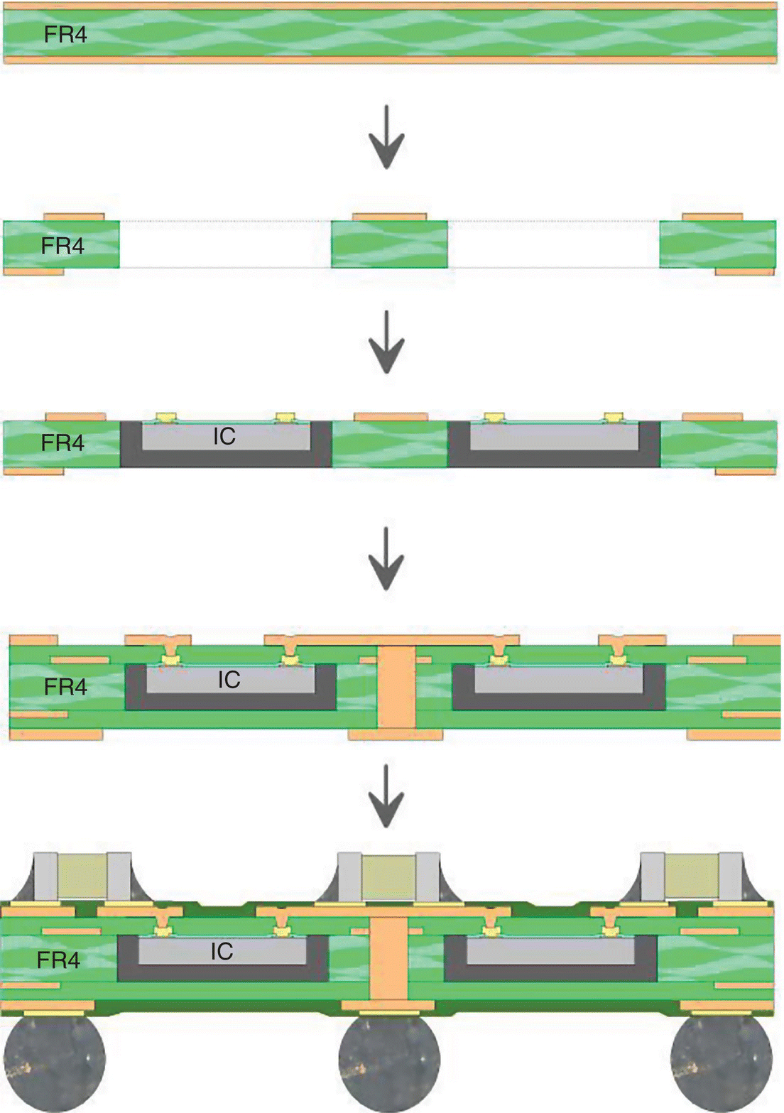
Figure 1.32 Imbera process flow for IMB.
The core layer was manufactured using normal inner layer PCB manufacturing processes like FR‐4 or bismaleimide triazine (BT). The active and passive components were placed using a nonconductive adhesive. An alignment tolerance of the assembly process of ±13 μm using a chip shooter with 7000 units per hour (uph) and ±5 μm using a FC bonder was published in 2004 and 2009 [38, 39]. The cavities were filled with a thermosetting epoxy to create a planar surface. Resin‐coated films (RCF) were pressed on both sides. UV laser drilling was used to open the vias to the components that need a minimum copper thickness of 3 μm on the I/O bond pads to withstand the process without damage. An example of the technology is shown in Figure 1.33.
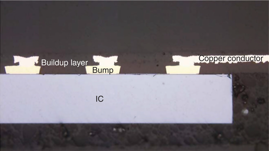
Figure 1.33 Cross section of embedded die using the Imbera process.
Several PCB process flows could then be used to build the modules. Due to the direct metallization of the I/O pads, a low contact resistance of less than 1 mΩ is possible. Thirty micrometer lines and spaces have been demonstrated. A slightly modified process flow was published in 2009 where the manufacturing process started with laser drilling micro‐vias and alignment marks into a metal foil (see Figure 1.34, step 1) [40].
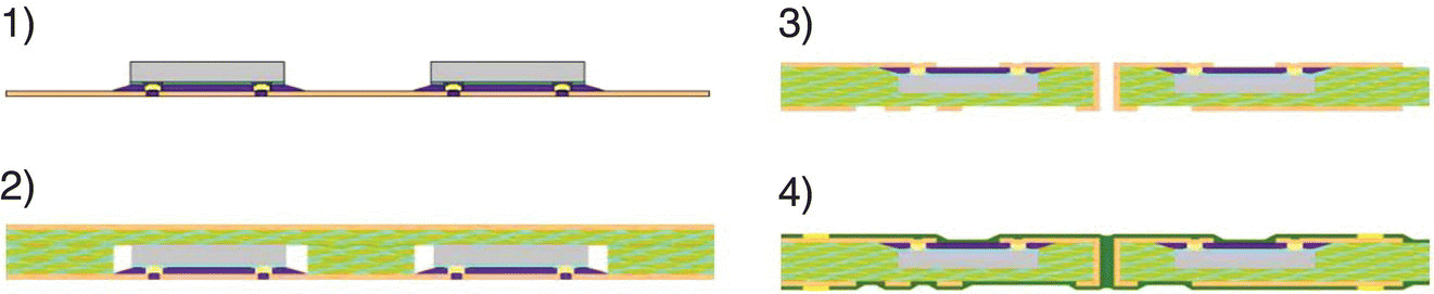
Figure 1.34 Process flow of the modified IMB process.
Prepreg with premanufactured openings around the components was pressed onto the foil and cured (step 2). The Cu foil and the laminate are patterned to form the electrical routing (steps 3 and 4). GE Healthcare Finland Oy, in partnership with GE Idea Works, announced in 2013 that it had completed the acquisition of Imbera Electronics Oy.
1.5 Fraunhofer IZM/TU Berlin Chip‐in‐Polymer (CiP)
A new concept for the integration of active components in organic substrates has been developed by Fraunhofer IZM and TU Berlin starting in the late 1990s. The chip‐in‐polymer (CiP) technology is based on the embedding of ultrathin chips into buildup layers of PCBs [41]. The interconnect structure, which is neither an FC nor a wire bond, is shown in Figure 1.35.
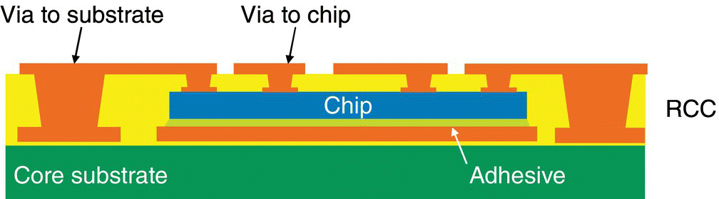
Figure 1.35 Interconnect principle of an embedded chip in a PCB buildup layer.
The basic idea of CiP is slotting thin semiconductor chips into standard PCB constructions. This technique can be used to fabricate 3D stacks of multiple die. The basic process flow is shown in Figure 1.36.

Figure 1.36 Process steps of chip embedding: (a) die bonding, (b) embedding in a polymer layer by vacuum lamination, (c) laser drilling of vias to chip and substrate, and (d) metallization of vias and Cu structuring.
The process started with the electroless Ni/Cu deposition on a wafer to strengthen the original bond pad [42]. Laser drilling of micro‐vias and the PCB metallization process are not compatible with Al or Cu contact pads of semiconductor chips. Therefore, a further layer of 5 μm Cu was applied to the bond pads of the chips to be embedded. Other metallization such as electroless Ni/Pd can be optimized for micro‐via plating. Passivation layers have to be tested for their fragility as well as for their adhesion with the resin‐coated copper (RCC) laminate layers. The wafers were thinned to 50 μm and diced. Die cavities were formed in FR‐4 PCB. The thinned chips were placed into 40 μm deep cavities. Placement accuracy is extremely crucial for chip embedding. The process tolerances for sequential die bonding via drilling and Cu structuring have to be very low in order to achieve an acceptable yield. One of the requirements is that the machines for these three process steps should use the same alignment fiducials on the core substrate. Especially large substrates are multilayer cores with small thickness and provide very low contrast to fiducial marks. Prior to chip placement, die ejection from a dicing blue tape takes place and should be optimized according to the adhesiveness of the tape, size, and ultimate thickness of the chip. Adhesiveness of the tape is regulated by UV exposure and is reduced for component pickup and placement without endangering the chip integrity. Additional requirements for the placement accuracy are related to the PCB vision system. The PCB camera has to cover the entire area of the proposed multilayer PCB cores as well as the problems related to the low contrast fiducial marks. Furthermore, a die bonder machine should have an advanced conveyor system. Chip bonding had been developed by using printable pastes and die attach films. Screen printing allowed a precise control of volume and location of the adhesive paste over dispensing. Electrically conductive Ag‐filled pastes or B‐stage pastes could be used. The core substrate with the die‐bonded chips was covered from both sides with an RCC layer. Temperature and pressure profiles should be adjusted carefully to promote epoxy adhesion at all interfaces and avoid chip breakage. A thickness of 15–20 μm over the chip surface was desirable for the subsequent micro‐via opening and filling. The overlaying Cu layer served as the base for package routing. In the CiP technology, interconnections were achieved via micro‐via laser drilling to chip pads and subsequent metallization, similar to the formation of micro‐via on PCBs. For micro‐via drilling, a pulsed 355 nm UV laser had been used. It could ablate Cu as well as the RCC dielectric. Accurate alignment of the micro‐via drilling with respect to the underlying Cu pattern remained challenging for the yield of the interconnection. After drilling, the micro‐vias were chemically cleaned and then treated by a Pd activation and electroless Cu deposition. The Cu layer was around 1 μm thick and acted as a seed layer for the consecutive Cu electroplating. A minimum thickness of 10 μm Cu was required in the micro‐vias. By the use of special Cu plating chemistry, a nearly complete filling of the micro‐vias could be achieved, as shown in Figure 1.37.
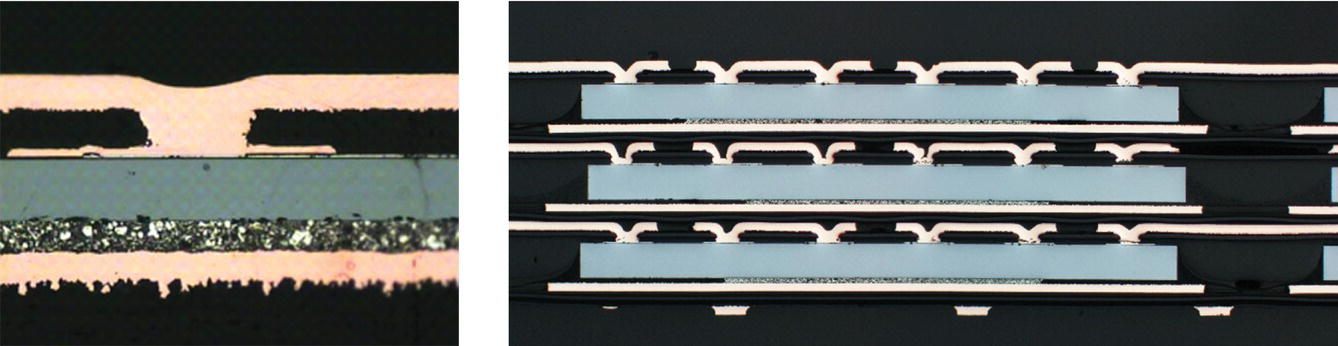
Figure 1.37 Cross section of a micro‐via interconnect to an embedded chip and three‐stacked embedded die.
An example of this embedding concept was a modular micro camera (see Figure 1.38) [43]. At a size of only 16 mm × 16 mm × 12 mm, including optics and 16 mm × 16 mm × 4.6 mm without the optics, the micro camera module is an extremely small system [43].
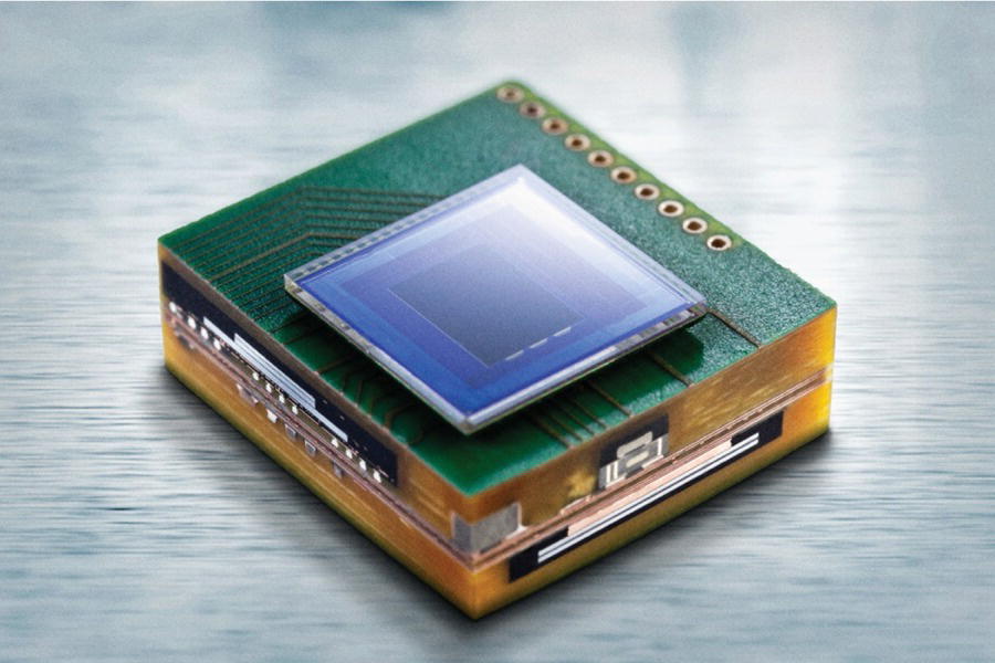
Figure 1.38 Cross section of the micro camera module with image sensor on top and processor embedded into the PCB.
A total of 72 passive and 13 active components (such as oscillators, DC‐to‐DC converters, memory chip, and image processor) have been embedded inside the module, and the image sensor is mounted on top. A key advantage of the newly developed module is that all components are integrated directly into the PCB. By encapsulating the electronic components, the micro camera is now impervious to any kind of environmental influences. The main system advantage is that the image material is directly inside the camera, since it is equipped with an integrated processor for image processing. After the image sensor has recorded the image, the integrated processor evaluates the frame. The video itself no longer has to be sorted and analyzed by an interposing system. Instead, only the relevant signals are transmitted. The data volumes to be transmitted and processed turns out to be much less.
1.6 HiCoFlex, Chip‐in‐Flex, and UTCP
The HiCoFlex process (see Figure 1.39) was commercialized by the company HighTec (Switzerland), which started in 1992 as an independent company, formerly being the thin film division of the Swiss company ABB [44].
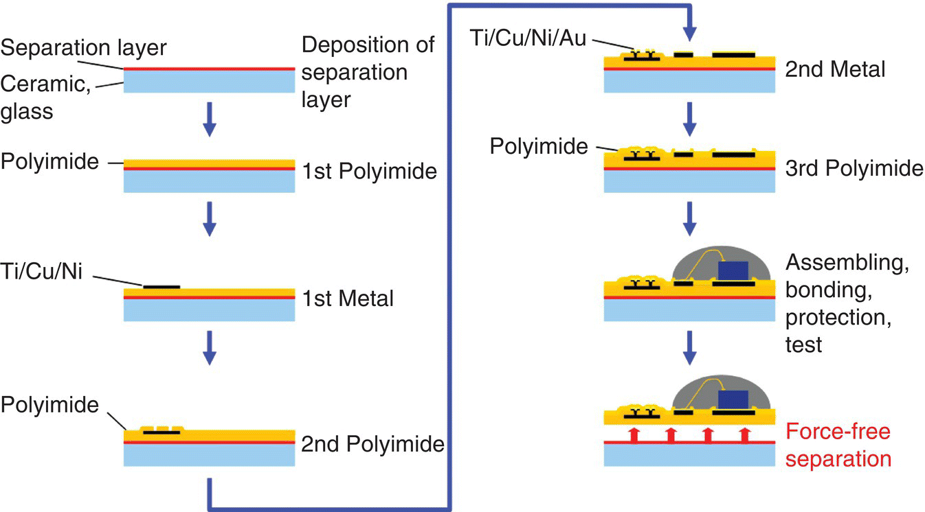
Figure 1.39 Process flow of the HiCoFlex process.
The process started with the deposition of a separation layer on a glass substrate. A multilayer PI and Cu process was added including active and passive components. After final testing and protection, the whole layer was separated from the glass substrate. The process was later transferred to 24 in. × 24 in. substrate size with 15 μm LDI technology. The technology is a kind‐of RDL‐first process.
Fraunhofer IZM and Technical University of Berlin (TUB) developed a Chip‐in‐Flex technology (FCF) [45]. By embedding chips into flexible wiring boards, the functional density of electronic systems can be dramatically increased. The benefits of flex substrates are light weight and high wiring density, which will be combined with the complexity of the active chip. However, to maintain the basic flex substrate characteristics, the buildup with an integrated chip has to be as small as possible. Chips with a thickness of only 20 μm have been used and the interconnection should not exceed a couple of microns. The technology relies on an FC‐type mounting of the thin chip onto the flex substrate and lamination of the structure on both sides (see Figure 1.40). Very thin chips (range of 20 μm) with Ni/Au pads are placed on 25 μm thin PI flex substrates using anisotropic conductive adhesive.
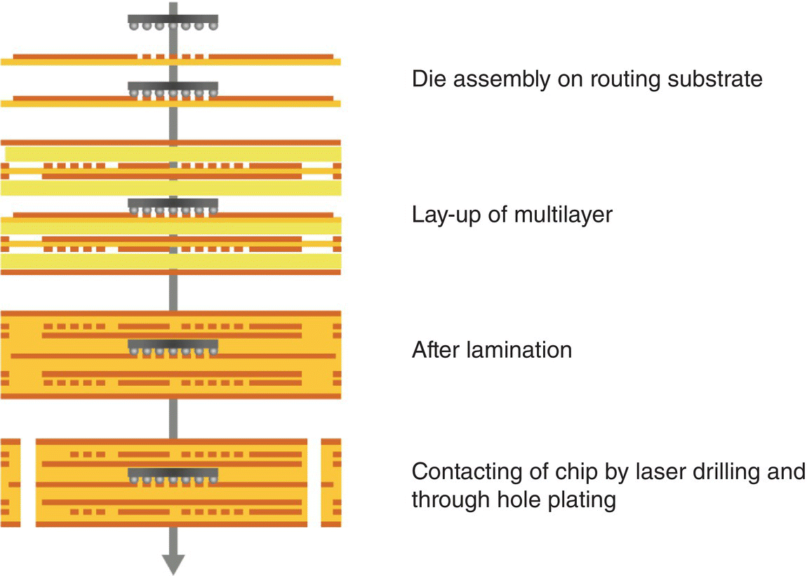
Figure 1.40 Process flow of the Chip‐in‐Flex technology.
Contacts to outer layers are realized by through‐holes. Further layers can be added to the buildup. The electrical interconnections are extremely thin, and the mechanical coherence of the chip to the substrate is ensured by the no‐flow underfill. After testing multiple flex substrates, the flex substrates are laminated together. Interconnections of the layers are done by laser drilling combined with a metallization process.
The ultrathin chip package (UTCP) technology developed by IMEC is based on the embedding of ultrathin die in flexible substrates [46]. The process flow is shown in Figure 1.41.
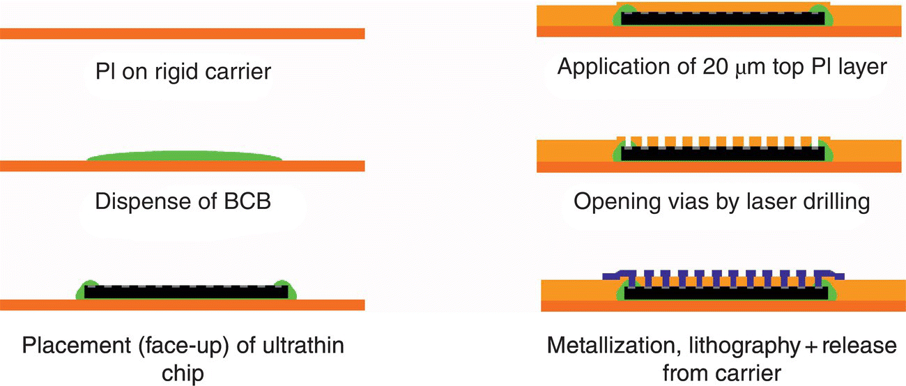
Figure 1.41 Overview of the process flow of the UTCP.
Chips with thickness in the range of 20–30 μm were packaged in between two PI layers. The result was a very thin and bendable chip package, with a total thickness of only 50–60 μm. The base substrate was a uniform spin‐coated PI layer, on a rigid carrier. Ultrathin chip are placed and fixed using BCB. A second PI process embeds the chips. Vias were made by laser drilling. The metal layer provides a fan‐out to the contacts of the chips. Finally the whole package is released from the rigid substrate. The potential for stacking in order to obtain 3D‐type chip packages is given by this process.
1.7 Conclusion
Embedding technologies and processes have a history of nearly 40 years. A majority of the fundamental work had been published by GE, mainly by Ray Fillion. The main driver at that time was the limitation of large monolithic ICs. In addition, a reliable bumping infrastructure that is now an industrial standard was not yet installed. Also, high density organic substrates were not available. Therefore, embedding was a valid alternative to FC, WB, and TAB for MCMs, offering excellent electrical performance with dense routing. One major issue for the embedding technology was and still is the lack of repair. Components that have been embedded are very difficult to remove. This is not the case for the chip‐last approaches like FC and WB. Therefore, one of the great advantages of today is the availability of KGD – one of the factors limiting the embedding process to only special application 30 years ago. These applications were mainly high‐end applications that required the very high performance of electronic systems using embedding technology. Most of the examples that have been described in this chapter are from this technology area. WB was the workhorse for consumer and personal computer products. With further miniaturization and increasing performance, WB is being replaced more and more by FC bonding. High density bumping processes were established, and the wiring density of organic substrates increased steadily. Over the last 10 years, the requirements for consumer, industrial, and automotive applications are strongly increasing. The differences in electrical performance for the different electrical interconnects are not negligible anymore. For example, the bandwidth for wired and wireless links is now increasing data rates by around 10 times every five years [47]. The Internet of things (IoT) is demanding a further steep increase in bandwidth. 5G is targeting 10–100 Gb s−1. Below 1 GHz, the electronic performance is not that different between the chip‐last interconnection technologies like FC and WB compared with the chip‐first direct chip connection using embedding. For example, the chip‐to‐package interconnection of the embedding process from TSMC (InFO) is based on copper bump without a solder joint. This reduces the loss between chip and package. Simulation results showed that parasitic R, L, and C of the embedding interconnection are 75, 76, and 14% lower from 55 to 65 GHz than those of the chip‐last technology using FC bonding [48]. Also the embedding technology from Amkor (SWIFT) has an improvement in cross talk and return loss by 6 dB at 2 GHz compared with an FC‐PoP [49]. Furthermore, a current motivation for the embedding process is the demand for packaging field‐programmable gate arrays (FPGA), which are ICs designed to be configured by the customer. Unfortunately, the manufacturing of large die like the FPGAs that are needed, for example, for artificial intelligence (AI) in the area of autonomous driving, is still limited by the process yield. Therefore, it may be cost effective to split a die into multiple die that are then reintegrated in a single SiP [50]. The Si yield curve is related exponentially to die area and a process‐specific constant (D0). Thus, for a given process technology, the cost advantage of a symmetrical die split into two die with equal areas of A/2 is then a function of the original single die area and the process yield (see Figure 1.42).

Figure 1.42 Cost advantage of die splitting for increasing die area and for different process yields [50].
Source: Reproduced with permission of Springer.
As shown in Figure 1.42, splitting a small die results in a smaller cost advantage compared with splitting a large die. However, for combining two or multiple die, a high‐speed interconnection like the embedding process is required.
In general, the high functionality in a small form factor together with superior electrical performance and high thermal dissipation are the major reasons for the restrengthening of the substrate‐less embedding technology. The cost of thin film routing has strongly decreased by the increasing wafer size. Also, high‐speed assembly has gained a significant high precision that has to be aligned to the fine line routing process. A step to panel‐level processing may further decisively lower the process cost for the high density embedding technologies.
References
- 1 Garrou, P. and Turlik, I. (1997). Multichip Module Technology Handbook. McGraw‐Hill Professional.
- 2 Bodendorf, D.J., Olson, K.T., Trinko, J.F., and Winnard, J.R. (1972). Active silicon chip carrier. IBM Technical Disclosure Bulleting 15 (2): 656–657.
- 3 Johnson, R.W., Davidson, J.L., Jaeger, R., and Kerns, D. (1986). Silicon hybrid wafer‐scale package technology. IEEE Journal of Solid State Circuits October: 845–851.
- 4 Te Velde, T.S. and Schmitz, A. (1968). Semiconductor circuit having active devices embedded in flexible sheet. US 3,579,056 A, registered on the 10 October 1968 and published 18 May 1971.
- 5 Fillion, R.A., Wojnarowski, R.J., and Daum, W. (1990). Bare chip test techniques for multichip modules. Proceedings 40th Electronic Components and Technology Conference (1990), pp. 554–558.
- 6 Gdula, M., Yerman, A., Krishnamurthy, V., and Fillion, R. (1993). The GE high density overlay MCM interconnect method solves high power need for GaAs system design. Proceedings of the Fifth Annual IEEE International Conference on Wafer Scale Integration (1993), pp. 339–345.
- 7 Fillion, R. (1993). A forecast on the future of hybrid wafer scale integration technology. IEEE Transaction CHMT 16 (7): 615–624.
- 8 Hannemann, R., Kraus, A., and Pecht, M. (1994). Semiconductor Packaging: A Multidisciplinary Approach, 156. Wiley.
- 9 Fillion, R., Wojnarowski, R., Gorcyzca, T., et al. (1994). Development of a plastic encapsulated multichip technology for high volume, low cost commercial electronics. Proceedings. 44th Electronic Components and Technology Conference (1994), pp. 805–809.
- 10 Vardaman, E.J. and Carpenter, K. (2007). Embedded active components and integrated passive. TechSearch International (October 2007).
- 11 Töpper, M., Wolf, J., Glaw, V. et al. (1996). MCM‐D with embedded active and passive components. Proceedings ISHM 1996, Minneapolis, USA (October 1996), pp. 224–229.
- 12 Töpper, M., Buschick, K., Wolf, J. et al. (1997). Embedding technology – a chip first approach using BCB. Advancing Microelectronics 24 (4): 18–22.
- 13 Mangold, T., Wolf, J., Töpper, M. et al. (1998) A multichip module integration technology for high‐speed analog and digital applications. Proceedings ISSSE Pisa, Pisa, Italy (September 1998), pp. 91–96.
- 14 Buschick, K., Glaw, V., Samulewics, K., and Karduck, C. (July 2001). Chip scale packaging of single chips for SMT assembly. PLUS (Produktion von Leiterplatten und Systemen) Magazine 1562–1572.
- 15 Buschick, K. (1995). Electric connections arranged in a high‐density grid. EP 0750791 A1 WO1995025346A1, PCT/DE1995/000359.
- 16 Ehrmann, O., Buschick, K., Chmiel, G. et al. (1995) 3D multichip modules. Proceedings of the International Conference on Multichip Modules (ICEMCM’95), CO (19–21 April 1995), pp. 358–363.
- 17 Wolf, J., Schmückle, F., and Heinrich, W. (1997). System integration for high frequency applications. Proceedings IMAPS Philadelphia, USA (1997).
- 18 Wolf, J., Schmückle, F., Heinrich, W. et al. (1998). System integration for high frequency applications. Proceedings Wireless Communication Conference, San Diego, USA (1998), pp. 37–46
- 19 Hahn, R., Kamp, A., Ginolas, A. et al. (1997). High power MCMs employing the planar embedding technique and microchannel water heat sinks. IEEE Transactions on CPMT‐Part A 20 (4): 432–441.
- 20 Buiculescu, V., Mannier, Ch.‐A., Oppermann, H. et al (2015). Micro‐fabricated hybrid package optimized for RF applications. Proceedings 16th International Symposium on RF‐MEMS and RF‐Microsystems, Barcelona, Spain (2015).
- 21 Töpper, M., Scherpinski, K., Spörle, H.‐P. et al. (2000). Novel manufacturing strategies in back end area. Proceedings of European IEEE/SEMI Semiconductor Manufacturing Conference (April 2000).
- 22 Töpper, M., Scherpinski, K., Spörle, H.‐P. et al. (2000). Thin chip integration (TCI‐modules) – a novel technique for manufacturing three dimensional IC‐packages. Proceedings IMAPS 2000, Boston, USA (September 2000), pp. 208–211.
- 23 Fritzsch, Th., Mroßko, R., and Baumgartner, T. et al. (2009) 3‐D thin chip integration technology – from technology development to application. IEEE International Conference on 3D System Integration, 2009. 3DIC (September 2009), pp. 1–8.
- 24 Töpper, M., Baumgartner, T., Klein, M. et al. (2009) Low cost wafer‐level 3‐D integration without TSV. Proceedings of the ECTC 2009, San Diego, pp. 339–344.
- 25 Baumgartner, T., Töpper, M., Klein, M. et al. (2009). A 3‐D packaging concept for cost effective packaging of MEMS and ASIC on wafer level. Proceedings of the EMPC, Rimini, Italy (15–18 June 2009).
- 26 Baumgartner, T., Töpper, M., Klein, M., and Reichl, H. (2010). Integration of thinned silicon chips in a polymer‐copper‐redistribution‐A‐3‐D stacking technology without TSVs. The Symposium on Polymers for Microelectronics, Winterthur, USA (May 2010).
- 27 Schmid, B., Gerner, M., Loreit, U. et al. (2011). Zuverlässigkeitsuntersuchungen an einem auf Waferlevel 3D umverdrahteten Raddrehzahlsensorsystem. Proceedings MST 2011, Darmstadt, pp. 253–256.
- 28 Kleff, J., Töpper, M., Dietrich, L. et al. (2013). Wafer level packaging for ultra thin (6 μm) high brightness LEDs using embedding technology. Proceedings IEEE‐ECTC 2013, Las Vegas, USA, pp. 1219–1224.
- 29 Carson, K. (1996). The emergence of stacked 3D silicon and its impact on microelectronics systems integration. Proceedings of the Eighth Annual IEEE International Conference on Innovative Systems in Silicon, Austin, TX (1996), pp. 1–8.
- 30 Couderc, P. (2012). SiPs in the medical domain and in the defense and industrial domain produced with WDoDTM technology. IMAPS Packaging Device Conference (March 2012).
- 31 Wakabayashi, T. (2003). System packaging and embedded WLP technologies for mobile products. Extended Abstracts of the 2003 International Conference on Solid State Devices and Materials, Tokyo (2003), pp. 386–387.
- 32 Braun, T., Raatz, S., Voges, S. et al. (2015). Large area compression molding for fan‐out panel level packing Proceedings ECTC, San Diego (2015), pp. 1077–1083.
- 33 Braun, T., Voges, S., Töpper, M. et al. (2015). Material and process trends for moving from FOWLP to FOPLP. Proceedings EPTC 2015, Singapore.
- 34 Braun, T., Raatz, S., Maass, U. et al. (2017) Kaynak development of a multi‐project fan‐out wafer level packaging platform. Proceedings ECTC, Orlando (2017), pp. 1–7.
- 35 Forman, G.A., Fillion, R.A., Kolc, R.F. et al. (1995). Development of GE's plastic thin‐zero outline package (TZOP) technology. Proceedings. 45th Electronic Components and Technology Conference (1995), pp. 664–668.
- 36 Fillion, R.A. (2006). Advanced Packaging Technology for Leading Edge Microelectronics and Flexible Electronics. Lecture at Cornell University.
- 37 Kujala, A., Tuominen, R., and Kivilahti, J.K. (1999). Solderless interconnection and packaging technique for active components. Proceedings 49th ECTC (1999), pp. 155–159.
- 38 Palm, P., Tuominen, R., and Kivikero, A. (2004). Integrated module board (IMB); an advanced manufacturing technology for embedding active components inside organic substrate. Proceedings 54th ECTC (2004), pp. 1227–1231.
- 39 Tuominen, R., Waris, T., and Nettovaara, J. (2009). IMB technology for embedded active and passive components in SiP, SiB and single IC package applications. Transactions of the Japan Institute of Electronics Packaging 2 (1): 134–138.
- 40 Tessier, T. G., Karila, T., Waris, T. et al. (2010). Laminate based fan‐out embedded die technologies: the other option. Conference Proceedings IWLPC 2010, pp. 198–203.
- 41 Aschenbrenner, R., Ostmann, A., Neumann, A., and Reichl, H. (2004). Process flow and manufacturing concept for embedded active devices. Proceedings EPTC 2004, Singapore (8–10 December 2004), pp. 605–609.
- 42 Ostmann A., Manessis, D., Stahr, J. et al. (2008). Industrial and technical aspects of chip embedding technology. Electronics System‐Integration Technology Conference, 2008. ESTC 2008, pp. 315–320.
- 43 Töpper, M., Wilke, M., and Ostmann, A. (2015). Integration technologies for image sensors. Imaging Conference Semicon Europa 2015, Dresden.
- 44 Godin, L. (2011). Miniaturization of medical devices thanks to flexible substrates. 1st Advanced Technology Workshop on Microelectronics, Systems and Packaging for Medical Applications, France (November 2011).
- 45 Löher, Th., Pahl, B., Huang, M. et al. (2004). An approach in microbonding for ultra fine pitch applications. Proceedings Technology and Metallurgy, The 7th VLSI Packaging Workshop of Japan, Kyoto (30 November–2 December 2004).
- 46 Christiaens, W., Vaandevelde, B., Bosman, E., and Vanfleteren, J. (2006). UTCP: 60 μm Thick Bendable Chip Package. Proceedings IWLPC 2006, pp. 114–120.
- 47 Nam, B.‐G. (2017). Digital Architectures and Systems Sub‐Committee Chair ISSCC Trends, San Francisco, USA (February 2017).
- 48 Hsu, Ch.‐W., Tsai, Ch.‐H., Hsieh, J.‐Sh. et al. (2017). High performance chip‐partitioned millimeter wave passive devices on smooth and fine pitch InFO RDL. Proceedings IEEE ECTC 2017, Orlando, USA, pp. 254–259.
- 49 Zwenger, C. (2017). Advancements in high fan‐out and heterogeneous integration. Proceedings Semicon Taiwan 2017.
- 50 Radojcic, R. (2017). More‐than‐Moore 2.5D and 3D SiP Integration, 5–67. Springer International Publishing ISBN 978‐3‐319‐52547‐1.