
10
Embedding of Power Electronic Components: The Smart p2 Pack Technology
Thomas Gottwald and Christian Roessle
Schweizer Electronic AG, Schramberg, Germany
10.1 Introduction
The electrification of the power train of hybrid electric vehicles (HEV) and electric vehicles (EV) increases the power demand and the power dissipation of power electronic modules. It is state of the art to use power modules based on ceramics such as direct bonded copper (DBC) or direct copper bonded (DCB) ceramic substrates because of the required combination of high ampacity, high insulation performance, and high thermal conductivity. In this conventional power module technology, bare die are assembled onto the topside copper of the DBC; the interconnection between power component and substrate and substrate to connector frame is carried out with thick aluminum (Al) wire bonds. Several wires have to be used in parallel to achieve the required ampacity of the modules. Figure 10.1 shows a typical power module for a three‐phase motor that consists of three DCB substrates (DCB: direct copper bonding) – one per phase – which are soldered onto a copper base plate. On the base plate, a plastic frame with connection pins is mounted, and the wire bonds connect the die to the DCB and the DCB to the frame.

Figure 10.1 State‐of‐the‐art three‐phase insulated‐gate bipolar transistor (IGBT) power module.
The number of process steps and the challenges for full‐area soldering of DCB substrates, wire bonding, and potting with the respective cost issues were accepted due to the lack of alternatives.
Increasing power density, increasing voltage, and the demand for higher switching frequencies require a closer look at the parasitic effects of such modules, especially the inductances. Not only static losses but also switching losses are of increasing importance. By increasing the switching frequency, the volume of passive components can be minimized, and therefore the total volume of inverters decreases. Higher frequencies, however, increase the corresponding switching losses. Overvoltage, which occurs after switching off the system, has a high potential of damaging the components.
One of the sources for parasitic inductances is the bond wires of conventional power modules due to the loops and their tolerances in shape, the number of bond wires, and their length. Another important issue for switching speed is the distance between gate driver and gate contact of the power component and their corresponding parasitic effects.
The bond wires are also critical with respect to reliability issues. Due to the huge difference in the coefficient of thermal expansion (CTE) between aluminum and silicon, one of the best evaluated failure modes is bond lifting from the surface of Si power devices. The higher the temperature cycle in the application, the sooner this failure will occur. The soldering joint of die to the DCB is a weak point in the design, too. This is one of the reasons why silver sintering is gaining interest for high reliability applications.
To solve the problem of the bond wires and of the soldering joints, leading manufacturers of power modules count on new technologies like silver sintering as a solder replacement for the interconnections between die and DCB, some also for the replacement of bond wires. Still, the expensive DCB substrates are part of those systems.
10.2 Technology Description p2 Pack
The p2 Pack technology is an embedding technology for power devices such as metal–oxide–semiconductor field‐effect transistor (MOSFETs) and insulated‐gate bipolar transistors (IGBTs) that produce significant power losses during operation and have a low number of electrical contacts. The source of power losses is switching losses and conduction losses of the power electronic components. The first trials of power semiconductor embedding have been made on the basis of the i2 Board technology, but even though it worked out to be feasible, it was not a very elegant approach for a component with a vertical current flow. The die attach and the heat dissipation needed an improved technological approach.
As the p2 Pack is very flat with a thickness of 1.2–1.7 mm, it is furthermore possible to embed this package into a PCB and realize the combination of power electronics and logic control in one single PCB without the need for additional connectors between logic and power.
As power and logic control act now in one board, this construction is called “Smart p2 Pack.” With the new p2 Pack technology, a new architecture was developed, which is helpful for very robust, cost‐efficient, and miniaturized high power inverter configurations.
10.3 Basic Package Construction
In Figure 10.2, the construction is shown in an exploded view of the layer stack. At the bottom, a base plate consisting of a copper layer is shown, which is covered by an insulating layer, made from a thermally conductive prepreg (a pre‐impregnated glass fabric, resin filled with thermally conductive inorganic fillers). The second level shows a lead frame with cavities. Inside the cavities, the power electronic components are assembled. The surface finish of the components is made from copper. The gray layer above consists of another thermally conductive prepreg and a copper layer, which has been patterned. The green layer is the logic control board into which the p2 Pack is embedded in a later step. It is a standard printed circuit board (PCB) that is used as control board for the power stage.
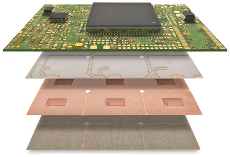
Figure 10.2 Exploded view of a Smart p2 Pack.
10.4 The p2 Pack Technology Process Flow
This newly developed technology uses embedding technologies and materials from the PCB industry. By using these technologies, very powerful and compact modules can be created, which lead to optimized electrical characteristics.
The starting point of this technology is lead frames with cavities that are assembled with power semiconductors, e.g. IGBTs or MOSFETs, as shown in Figure 10.3. The die attach is carried out with either diffusion soldering or transient liquid phase bonding (TLPB). Also sintering processes like silver sintering are possible. After assembly, the surface of the die and the surface of the lead frame are planar. In Figure 10.4, an assembly of six MOSFETs on a lead frame can be seen. They are already arranged in a way to form a three‐phase B‐6 topology for a motor drive after finishing the assembly.
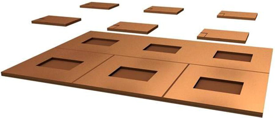
Figure 10.3 Process flow: lead frame with cavities where power devices are assembled into the cavities.
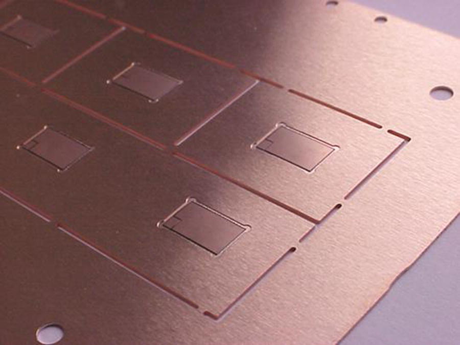
Figure 10.4 Lead frame with power MOSFETs assembled into cavities.
These assembled lead frames are laminated into a three‐layer construction with an electrically insulating material on top and bottom of the lead frame (layer 2). The outer layers consist of copper sheets (layers 1 and 3) and work as a heat spreader at the bottom, while the top layer acts as a routing layer that replaces the bond wires used in ceramic power modules.
Figure 10.5 shows the top side of a B6 module, where six MOSFETs are arranged and electrically routed for a three‐phase motor drive. The interconnection to the gate/source contacts is carried out with blind vias, which are drilled with laser drilling equipment through the dielectric layer and filled with copper in a galvanic Cu‐plating process. The drain contact is mechanically and electrically connected with the lead frame. The lead frame can either be directly attached after routing off the cover layers to the lead frame level, or it can also be connected to the top layer with electroplated blind or through vias.
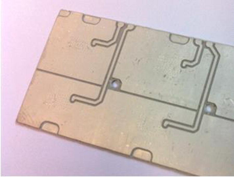
Figure 10.5 B6 bridge module. Gate/source connection with copper traces/planes.
Figure 10.6 shows a cross section of a p2 Pack. The bottom layer represents the insulated copper base plate, which can be directly attached to a heat sink. The middle layer is the lead frame with a small cavity of 70 μm with an assembled power MOSFET of the same total thickness. The thickness of the lead frame can be adapted to the needs of the application in terms of heat dissipation. The top layer is the routing layer for the interconnection of the top contact gate and source to the top layer carried out with copper‐filled blind vias. The black layers are built with dielectric prepreg sheets and guarantee the insulation at those places where they are not penetrated with blind vias. The copper surface of the component ensures a highly reliable metal to metal adhesion with superior electrical and thermal conductivity.

Figure 10.6 Cross section of a p2 Pack with copper‐filled blind vias.
One of the preconditions for the power devices is a surface plating of copper on the contacts of the device. This is necessary for the plating compatibility. The construction of the p2 Pack is symmetric, which leads to a minimized warp and twist during thermal cycling and therefore minimizes pump out effects of thermal interface material (TIM), when it is directly mounted to a heat sink. The thick copper layers above and below the lead frame lead to an optimized heat spreading in each layer and in fact to a double‐sided cooling of the power device. Up to one‐third of the heat is transferred to the top layer and from the top layer through the complete package to a heat sink connected from the bottom side.
10.5 Smart p2 Pack
The p2 Pack itself can be used as a one‐to‐one replacement of existing DCB substrates in combination with already existing logic control boards. Due to the fact that the p2 Pack is as flat as 1–1.4 mm, it is possible to go one step beyond and embed such a flat component into a logic control board. By doing so, very short interconnections from the gate driver to the gate contact of the power device are feasible. The driver component can be placed on the control board directly above the power semiconductor, while the connection to the gate is made with copper‐plated blind vias from the outer layer to the p2 Pack. The Smart p2 Pack construction is open to the bottom side of the PCB. A heat sink can be easily installed to the bottom side, either using a TIM or using sintering technologies to further reduce the thermal resistance from junction to ambient.
10.6 Package Performance
10.6.1 Electrical Performance
Chip embedding technologies are used to embed thin bare die (MOSFETs or IGBTs) into a construction of lead frames and additional routing levels. The interconnections are carried out with blind vias that are filled with electrolytically plated copper that reduces the package‐related resistance Ron. Ron is the resistance of the package consisting of chip resistance, bond wire, and lead frame resistance. The blind vias also reduce the parasitic inductances to a minimum. Measurements showed an improved Ron where the complete p2 Pack had almost the same Ron as the chip itself. By using blind vias instead of bond wires, the package‐related part of the Ron could be reduced by a factor of 100 and is difficult to be measured correctly. The difference in package resistance is pointed out in the respective data sheets for embedding components in comparison with packaged components (Figure 10.7).

Figure 10.7 Data sheets indicating the Rdson (drain to source on state resistance) for embedded components (left) and packaged components (right) for the same die size and chip technology.
Figure 10.8 shows the results of total resistance measurements of the same power electronic component. On the right, the chips were packaged in a TO 263 package with seven leads. In the middle (dotted line), the chips were mounted on a DCB substrate and wire‐bonded to a connector frame. On the left, the chips were embedded into a PCB and connected with copper‐filled blind vias. Each point represents the measurement result of one component. The graph is displayed as a probability plot. In this case, the total Rdson could be reduced from 1 to 0.5 mΩ, which is close to the theoretical chip resistance. This means there is almost no package‐related resistance left.
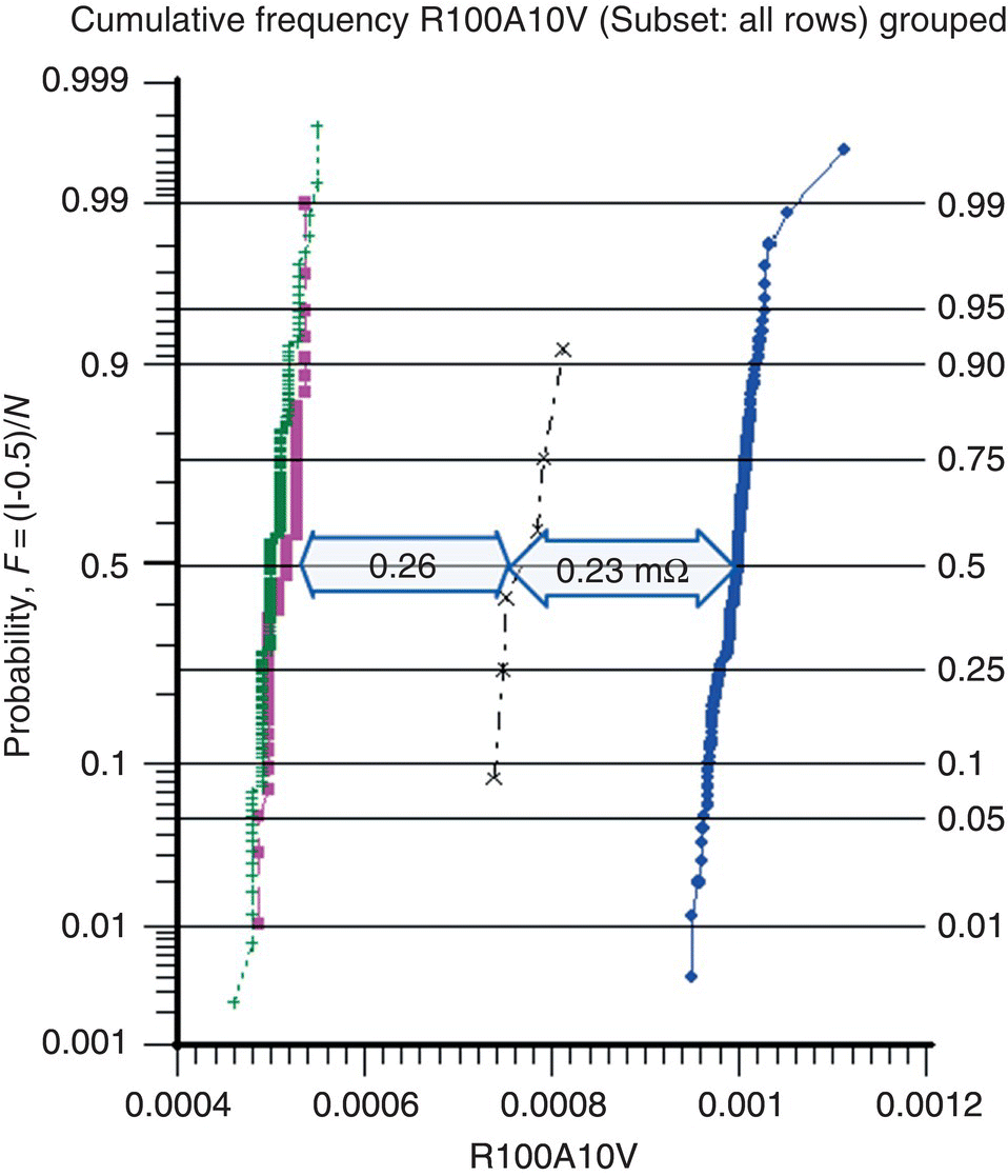
Figure 10.8 Rdson for TO 263‐7 (right), die on DCB substrate (middle), and p2 Pack (left).
10.6.2 Dynamic/Switching Losses
Faster switching speeds for power electronic assemblies are desirable for many reasons. The faster the switching, the smaller the component size of passive components like capacitors and inductors can be. This effect is beneficial in terms of miniaturization and cost involved. The drawback of faster switching is an increase of the dynamic losses of the system, which makes it less efficient. Several embedded dies in the p2 Pack technology have been tested for switching speed in comparison with DCB‐based power modules. Figure 10.9 shows the faster current rise and fall times that are indirect indicators for lower inductances in the p2 Pack system.
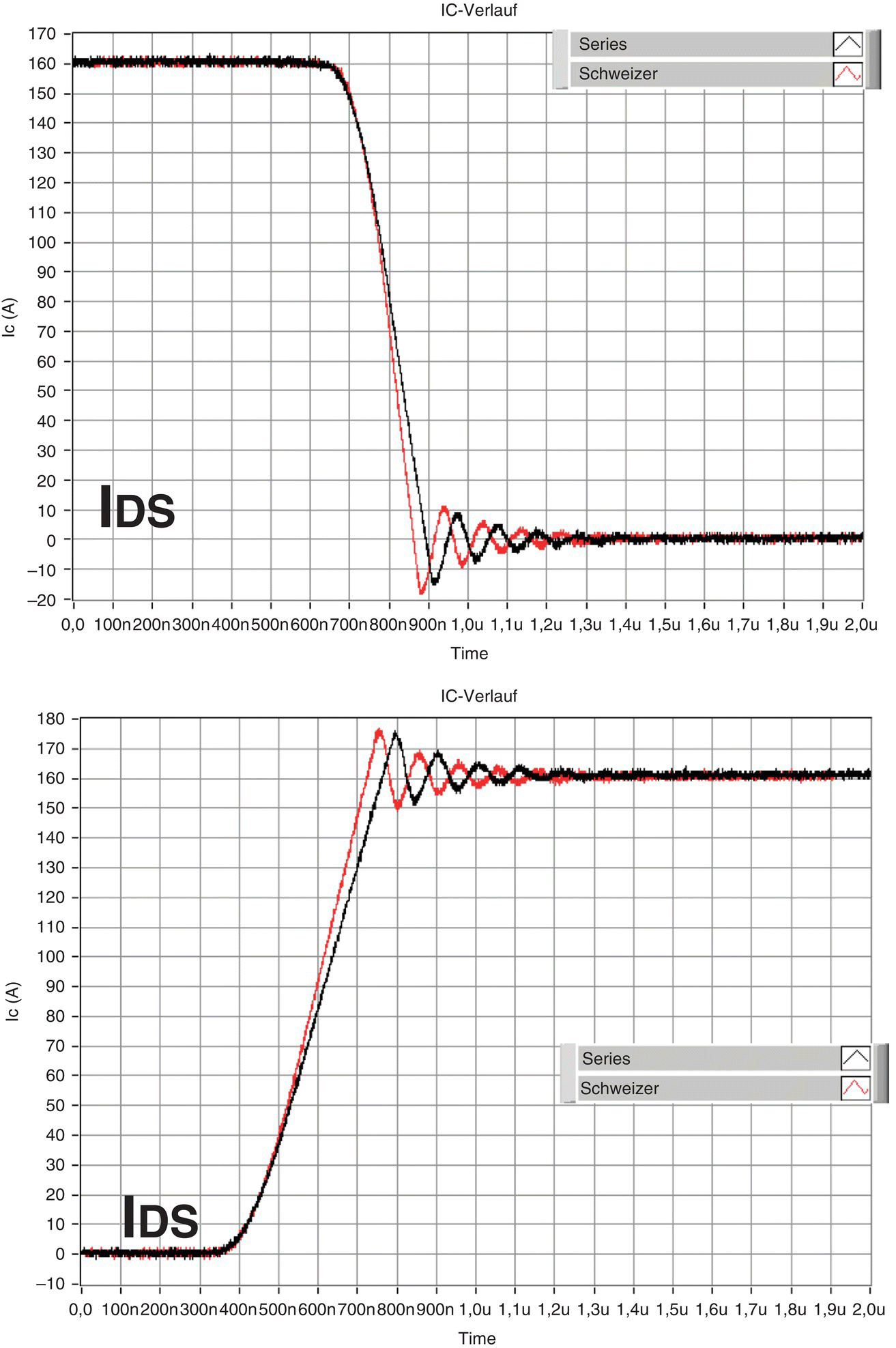
Figure 10.9 Switching characteristic of p2 Pack (gray) vs. die on DCB (black) at 160A: 12% faster switching.
10.6.3 Inverter Efficiency
A complete inverter for a 32 kW engine was designed and built with ETH Zurich. It uses 1200 V IGBT components and recovery diodes and consists of a classical B6 topology (see Figure 10.10). The inverter was built with two separate PCBs in this state of the development, one for the control (top) and one for the power stage (bottom) as the measurements for the characterization of the inverter were much easier to be carried out due to an easier access to measurement points on the PCBs. In a next step, this inverter will be built in one single PCB as Smart p2 Pack. The DC‐link capacitor was made from a block of foil capacitors at the bottom of the assembly. The cooling of the semiconductors was carried out by attaching a water cooling unit beneath the power stage (hose connection on the right).

Figure 10.10 32 kW test vehicle in Smart p2 Pack technology. IGBT application.
The Smart p2 Pack inverter was completely characterized and performed at a very high efficiency. Figure 10.11 shows the inverter efficiency at a switching speed of 10 kHz and different gate resistors. Although the inverter could only be tested up to 18 kW, it showed an efficiency of almost 98%, while the efficiency graph was still rising toward higher power; therefore higher efficiencies at full load can be expected.

Figure 10.11 Efficiency graph of a 32 kW test vehicle in Smart p2 Pack technology at partial load conditions.
10.6.4 Thermal Performance
The p2 Pack technology was designed for superior thermal performance. The basic concept is to add a heat spreader of the same size to all power electronic components embedded into a laminate. By spreading the heat with the lead frame before transferring it through the insulating material, a very low thermal resistance (Rth) can be achieved.
To analyze the thermal dissipation in the p2 Pack, a finite element (FE) simulation model was built and calculated with different variables. To reduce the calculation time for such a model, it is very common to simulate only ¼ of an object, as long as it is symmetrically built (see Figure 10.12). This was also done with the underlying simulation, whose results are shown in Figure 10.13.
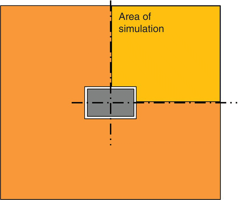
Figure 10.12 Symmetry areas for FE modeling: ¼ of a lead frame assembled with a power semiconductor in the middle.

Figure 10.13 Temperature distribution and thermal resistance (Rth) in a p2 Pack single cell assembled on a heat sink.
Figure 10.13 shows the calculated temperature distribution of a FE model of ¼ of a p2 Pack in a cross section. The front left corner represents the chip center, while the edges represent the cross‐sectional lines through the package. The dark layer at the bottom represents a heat sink that is installed beneath the p2 Pack. Between the p2 Pack and the heat sink, a TIM was designed into the model with a thermal conductivity of 1 W mK–1. The TIM was the most critical material due to the highest contribution to the thermal resistance. Almost 50% of the total thermal resistance (Rth) came from the TIM. This gives a lot of potential for improvement of the system.
The larger the lead frame is, the better the thermal performance will be. Further simulations have shown that a factor of 4 to 1 in area for lead frame to chip area is a good starting point to balance thermal performance with cost for the lead frame and design area needed to place the embedded components.
10.6.5 Robustness and Reliability Data
The p2 Pack went through a full component qualification as well as a full PCB qualification. Before testing, preconditioning was carried out with moisture sensitivity level 3 (MSL 3) with three reflows at a peak temperature of 260 °C [1]. The most critical tests in terms of reliability are the reflow soldering after exposure to humidity (MSL3), the thermal shock, the active load cycling, and the hot storage test. Temperature cycling was performed with two‐chamber reliability equipment with 30 minutes at 150 °C and 30 minutes at −55 °C per cycle with a transfer time of <10 seconds. Active load cycling was accomplished by running high currents through the semiconductor and heating up the probe due to the component resistance Ron. A typical cycle was two seconds on and then two seconds off. The temperature difference between the on and off states was 80 K. Hot storage means holding the probes at a temperature of 175 °C for at least 1000 hours. Tests up to 2000 hours were also performed. All component and PCB‐related qualification requirements could be achieved without failure. The reliability in active load cycling was found to be at least 10 times higher than a power module built with ceramic substrates. Up to 2 M cycles with a temperature difference of 100 K could be demonstrated, before the test was finished without damage. Typical values for ceramic‐based power modules are 80k to 120k at an 80 K temperature difference.
10.7 Applications and Markets
The first generation of p2 Pack products will be based on low‐voltage MOSFETs from Infineon, which were especially designed for embedding applications. The qualification is done at automotive level as the first applications are expected to start in this market. The technology is not in production as of publication, since automotive design cycles take several years, especially for completely new technologies, but it is expected to find its first applications under the hood. At the moment Schweizer is preparing a plant for mass production. Meanwhile the next‐generation p2 Pack for wide bandgap semiconductors is in development. Very low loss components like gallium nitride (GaN) and silicon carbide (SiC) need to have a low‐inductance package like the p2 Pack; otherwise the advantages of the new semiconductor technologies cannot be exploited.
10.8 Summary
The advantages of the p2 Pack chip embedding technology are manifold. The technology began with the attempt to miniaturize power electronics and improve thermal dissipation; however, many additional benefits were found. It is obvious that miniaturization can be easily achieved for the x/y‐direction as well as for the z‐direction. The heat dissipation could be improved by 30–44% in comparison with a DCB substrate at the same size, and the thermal resistance junction to heat sink of 0.5 K W−1 was achieved [2].
Today’s power electronic systems consist of several substrates and a collection of interconnect technologies. With the Smart p2 Pack, the whole assembly can be manufactured by means of surface‐mount technology (SMT), which makes the assembly easier to control in high volume manufacturing and more robust than conventional systems. The losses can be minimized, as the static and the dynamic losses are lower for embedded constructions compared with conventional systems. This increases the energy efficiency of the system and reduces the efforts to spend for the cooling system. The p2 Pack and the Smart p2 Pack can be built as electrically insulating systems. Therefore the backside of the boards can be directly assembled onto a heat sink. The choice of TIM is open to the customer and electrically conducting TIM is also available.
A very nice feature is the very low inductance of a p2 Pack. The low inductance enables fast switching in a pulse‐width modulation (PWM) mode. For some applications, faster switching offers the possibility to reduce the size of the passive components and cost involved. It also offers the opportunity to reduce the voltage class of power devices in the application. Today 650 V IGBTs are being used in drive applications although the DC‐link voltage is set to 400 V. The margin of an additional 250 V blocking voltage is needed to control the voltage overshoot after switching on or off. The reason for this overvoltage is the parasitic inductance of today’s systems, which is 5–10 times higher than with a p2 Pack. If 450 V devices could be used in those systems, because overvoltage is reduced due to low inductances, the Ron of these components would be reduced by approximately 30%, which would increase the system’s energy efficiency and reduce the cooling efforts.
One of the biggest assets of the technology is its extremely high reliability. The robustness in active load cycling could be improved by a factor of 10 compared with conventional wire‐bonded power modules on DCB substrates.
Acknowledgments
The authors acknowledge the competent contribution of Infineon Technologies and ETH Zürich to this work.
References
- 1 IPC/JEDEC J‐STD‐020E (2014). Moisture/reflow sensitivity classification for nonhermetic surface mount devices (December 2014).
- 2 Kearney, D., Kearney, D.J., Kicin, S. et al. (2016). PCB embedded power electronics for low voltage applications. 9th International Conference on Integrated Power Electronics Systems, Proceedings (8–10 March 2016), Nuremberg, Germany.