
21
Temporary Carrier Technologies for eWLB and RDL‐First Fan‐Out Wafer‐Level Packages
Thomas Uhrmann and Boris Považay
EV Group – St. Florian am Inn, Austria
Fan‐out wafer‐level packaging (FO‐WLP) process flows typically fall under two basic integration categories called chip‐first and chip‐last. With the chip‐first approach, individual chips are embedded into epoxy mold, forming freestanding molded wafers as a basis for redistribution layers (RDL) and bumping, referred to as embedded wafer‐level ball grid array (eWLB). In the chip‐last approach, RDL are processed first, before the die are individually attached and overmolded. In both process flows as shown in Figure 21.1, temporary wafer carrier technologies play a crucial role. For chip‐first (or RDL‐last), temporary carriers are used for package‐on‐package (PoP) technology, where thinning device wafers below 400 μm does not allow for the use of freestanding molded wafer handling, as discussed by Campos et al. [1–3]. Slide‐off debonding has been found to work reliably within the molded wafer process flow.

Figure 21.1 Schematic manufacturing process for chip‐first and chip‐last integration, including the use of temporary carriers.
For eWLB, the warpage of the molded substrates is generally one of the biggest challenges for high volume manufacturing. The different coefficient of thermal expansion (CTE) for silicon and mold compound will cause each product to behave slightly differently in terms of intermediate thermal expansion. Especially, changes in terms of molded wafer thickness, die content, die location, die spacing, and height distribution introduce variation from product to product [3]. Furthermore, reduction of molded substrate thicknesses below 400 μm will cause the reconstituted wafers to acquire a flexible behavior that no longer allows self‐support and freestanding handling. Also, reducing the wafer thickness often increases z‐axis asymmetry, adding nonlinear behavior to the already flexible wafer. Processing such wafers makes temporary bonding of the thin molded wafer to a carrier an inevitable step, serving as pure mechanical support during processing. Depending on the carrier material, different adhesive types and respective debonding methods can be used.
Contrary to this, chip‐last is a pure buildup process, where the temporary release film forms the base layer. The package is built successively on top of the carrier wafer, and UV laser debonding is the final process step separating the devices from the carrier; hence fundamental knowledge of critical process parameters for UV laser debonding is the key to ensuring a high overall process yield.
Temporary wafer bonding is classified by the mechanisms that break the temporary bond interface and their point of interaction: direct chemical bond release by laser radiation (laser debonding) via ablation or gas generation or elevated temperature to soften or at higher levels to thermally dissociate the adhesive layer (slide‐off and lift‐off debonding). Notably, the debonding temperature is only linked to the debonding mechanism for slide‐off and lift‐off debonding, while laser‐initiated debonding decouples the debonding mechanism from the global process temperature. Figure 21.2 provides more detail on each debonding process.

Figure 21.2 Classification of temporary bonding and debonding processes.
Depending on the integration process flows for FO‐WLP, requirements for temporary bonding differ, separating into laser‐initiated debonding of RDL‐first buildup packages, while slide‐off and lift‐off debonding is used for chip‐first packages to process molded substrates.
21.1 Slide‐Off Debonding for FO‐WLP
Temporarily attaching the molded reconstituted wafer to a suitable carrier was adopted to overcome the warpage and flexibility by stabilizing the molded wafer and reducing its topography variations. The selection of a carrier wafer and its dimensions, as well as of adhesive materials, is the key element to a successful temporary bonding and debonding technique. Epoxy‐based mold compounds typically have high and nonlinear CTE. On account of these, several different carriers with different CTE, stiffness, and carrier thicknesses were evaluated, as shown in Table 21.1. Overall, the carrier CTE should closely match the molded wafer CTE under all different processing conditions. The nonlinear CTE of the mold compound should match well for low temperature processes. On the other hand, for high processing temperatures over 200 °C, the CTE of common molds exceed values of 15 ppm. In this process temperature range, the adhesive material has to absorb the additional stress.
Table 21.1 Mechanical properties of carrier materials for temporary bonding in FO‐WLP.
| Mechanical properties | Carrier materials | ||
| Glass | Silicon | Ceramic | |
| CTE (ppm °C−1) | 7.8 | 2.6 | >8.0 |
| Young’s modulus (GPa) | 74 | 130 | >300 |
| Carrier thickness range (μm) | 700 | 600–700 | 550 |
Once these preliminary steps are done, an adhesive is applied on the carrier or through spin coating or lamination. The nature of the adhesive and its deposition method is crucial to bonding success. As semiconductor processing involves a variety of different chemical, thermal, and plasma processes, selecting the right adhesive is essential, and very often material properties and functions are contradictory. Proficiency in temporary bonding and debonding involves several parameters, the first of which is the initial condition of the wafers. The final bonding quality (i.e. success in attachment and detachment) is dependent on a combination of parameters such as temperature, atmosphere, chemical exposure, and mechanical stress of the post‐temporary bonding process, as well as total thickness variation (TTV), the presence of particles and voids, bow and warp, and the centricity of the wafers. These characteristics will help define the adhesive and process to be used.
Polymers are classified into two families: thermoplastics and thermosets. Thermoplastic adhesives have the ability to be solidified and re‐melted, which is their key differentiator over thermosetting polymers, whose solidification is irreversible. In contrast thermoplastic residues can be chemically removed after debonding, which reduces contamination for the rest of the process. The maximum permitted operating temperature in the bond interface and the required rigidity are the most decisive parameters, as the adhesive layer has to remain stable throughout the process, especially for processes that involve heat and strong mechanical stress such as backgrinding.
TTV after temporary bonding is of central importance to bonding. Any local thickness variation of the temporary adhesive will be transferred to the device wafer. TTV variations mainly stem from spin coating and baking uniformity issues during the application of the adhesive film and pressure uniformity issues during bonding. Additionally, the adhesive must be compliant with the debonding process, which tends to require room temperature conditions.
The development of bonding processes for FO‐WLP has been guided by restrictions of the molding and the RDL fabrication process steps. The correlation between increasing mold stress and rising temperature has fostered the adoption of low temperature adhesives, making thermoplastic adhesives an appropriate solution. Because of the initial warpage of the molded wafer, materials with high adhesion characteristics were considered to maintain a plain contact between the carrier and the mold and to prevent delamination. Finally, the RDL fabrication and its chemical environment have also influenced the choice of the adhesive material.
Besides the temporary adhesive, the carrier wafer properties determine the stability and process cornering of the temporary bond and debond step. These are primarily (i) thermal compatibility of the carrier substrate to the FO‐WLP device wafer to minimize stress upon their interface (CTE mismatch across the whole operation temperature range), (ii) mechanical properties such as high strength and stiffness to ensure sound support and to enforce flatness to the set wafer carrier, and (iii) chemical stability in harsh chemical environments imposed by the FO‐WLP process such as etching and electroplating.
Based on the results obtained during extensive experiments, some common carrier materials were found to be inadequate, and new types of carriers, together with the most suitable matching temporary bonding adhesives and process conditions, were found to meet the demand. After careful selection, the best combination of such parameters enabled a robust temporary bonding solution for FO‐WLP. No visual or internal abnormality was seen on the optimized configuration, and minimum wafer warpage was measured during critical FO‐WLP process steps [3].
As a result, the right carrier technology has been found as a combination of carrier material, carrier thickness, and adhesive properties. In terms of carrier material, the CTE as well as material stiffness has to be high. For these reasons, silicon and glass carriers do not fit well as carrier material for mold‐first, RDL‐last FO‐WLP. In addition, the high stress level during processing demands an increased carrier thickness of 1.0–1.3 mm, in order to reduce bow and warp levels after processing. A last main determining factor is the adhesive. The layer thickness as well as viscosity under process conditions, or material rheology, determines the maximum process temperature. Thinner adhesives undergo less material flow during processing and hence lead to a larger process window.
Finally, process conditions have to be adapted to work with carrier‐mounted FO‐WLP. As the carrier system is much thicker, including several different materials with different thermal conductivity, temperature ramp up and ramp down, for example, in deposition processes, have to be lowered to provide strain relaxation in the carrier system.
21.2 Laser Debonding: Universal Carrier Release Process for Fan‐Out Wafer Packages
UV laser debonding has several advantages over other debonding techniques that make it an extremely flexible debonding process. For slide‐off debonding, material properties such as glass transition and material softening determine bonding, debonding, and maximum process temperature. In the case of laser‐induced debonding, even permanent adhesive films with suitable photoactive response can be used. Hence, the debonding process is a decoupled function of the carrier system. Due to the well‐controllable optical interaction, a wider range of chemical and physical parameters, such as spectral absorption and photosensitivity, scattering, or reflectivity can be utilized to separate the response of the different layers. This way, the individual process requirements, including high temperature, tension, or pressure, can be supported when selecting the optimal adhesive combination. Further flexibility can be achieved by adding functionality to the debond layer that also protects the substrate from side effects like thermal or mechanical stress, nonplanarity, or contamination. In contrast to mechanical or slide‐off debonding where the adhesives are engineered for embedding of structures and adhesion to surfaces and also include the debonding trigger, this is not the case for laser debonding. The adhesive in laser debonding has no additional function for the debonding process, but is solely responsible for detachment after photoactivation. The only exceptions to this rule are polyimides. Their chemical structure allows for embedding and bonding of the materials and also acts as the photoactivated UV laser debonding layer. Meanwhile, their process latitude or temperature process window allows for very high thermal temperature stability (approaching 400 °C), and the material has high absorption at the laser debond wavelengths and also dissociates during UV exposure and so does not debond as easily as a material developed for very low levels of laser‐initiated decomposition. During the other process steps, the material is almost inert.
The high independency of the laser debond process from the rest of the process flow, compared with mechanical or slide‐off debonding, allows for a much more straightforward integration of temporary carrier technology. Another key benefit of UV laser debonding is its insensitivity to different substrate types, passivation layers, and metals. Laser debonding confines the temporary adhesion function to the carrier substrate side and does not impose additional limitations on the substrate, other than the ability to bond itself. Other debonding techniques rely on surface energy during adhesion or release, temperature behavior, solvent permeability properties, or defined release at specific stress levels of the bonded surfaces to ensure proper debonding. In contrast, UV debonding relies solely on the selective decomposition of the laser release layer. The substrate is kept at room temperature during debonding, meaning no thermal activation is needed. This allows for the use of a wide variety of temporary bonding adhesive types, which can be made with very low adhesion properties since the separation of the product wafer from the carrier wafer is force‐free after debonding. The combination of this instantaneous bond release, avoidance of the thermal activation step, and high scanning speed associated with UV diode‐pumped solid‐state (DPSS) lasers allows increased debonding throughput compared with other debonding techniques. A drawback of laser debonding is that it requires a UV transparent glass carrier in order to allow the laser light to initiate the laser debond process at the bond interface. However, where sodium ion contamination or mismatch of glass properties have been issues with this approach in the past, glass manufacturers can now offer suitable glasses that eliminate these obstacles.
Table 21.2 gives an overview of available UV laser debonding technologies today. Predominantly two different types of lasers are found for laser debonding today, namely, gas‐based excimer lasers and DPSS. Excimer lasers offer high power with a beam that can be formed into rectangular or square shapes with a uniform power density. However, they come with high maintenance and footprint. In the last couple of years, DPSS lasers have closed the power gap, are cheaper to maintain, and have a smaller footprint. However, they come with a Gaussian beam profile, as sketched in Table 21.2. In this case, the energy distribution leads to debonding around the full width at half maximum of the Gaussian beam shape. Around the maximum, the excess energy leads to burning of the debond layer. For this reason, the further discussed system features a DPSS laser with a flat‐top beam profile, delivering a uniform debond at low system and process cost.
Table 21.2 Comparison of UV laser sources for debonding in terms of their respective benefits and drawbacks as well as schematic beam profile.
| Solid‐state laser | Excimer laser | ||
| Gaussian beam profile | Flat‐top beam profile | ||
| Pro |
|
|
|
| Con |
|
| |
| Beam profile |
![Gaussian beam profile of radiant exposure [a.U.] vs. x [a.U.] displaying a vertical rectangle formed inside a parabolic curve.](http://images-20200215.ebookreading.net/2/1/1/9781119314134/9781119314134__advances-in-embedded__9781119314134__images__c21uf001.gif) |
![Flat‐top beam profile of radiant exposure [a.U.] vs. x [a.U.] displaying a vertical rectangle formed inside a top-hat shape.](http://images-20200215.ebookreading.net/2/1/1/9781119314134/9781119314134__advances-in-embedded__9781119314134__images__c21uf002.gif) |
![Excimer laser beam profile of radiant exposure [a.U.] vs. x [a.U.] displaying a horizontal rectangle formed inside a wider a top-hat shape.](http://images-20200215.ebookreading.net/2/1/1/9781119314134/9781119314134__advances-in-embedded__9781119314134__images__c21uf003.gif) |
21.3 Parameters Influencing DPSS Laser Debonding
To limit the thermal input associated with laser debonding, UV DPSS lasers are favored for the debonding step, since they provide the benefit of rapid absorption of the UV light immediately at the glass release layer interface and also allow for direct photochemical interaction at chemical bonds provided by readily available materials. Ideally, release layer materials feature a high absorption coefficient in the relevant wavelength regime around the laser wavelength, typically situated around the well‐known frequency‐tripled Nd:YAG laser emission at λ ≈ 355 nm. In this case, penetration depth of light is limited to less than 200 nm for most commercially available debond materials. Furthermore, due to the limited peak power of these lasers, it is essential that the transmittance toward the bond interface is high and their radiation can be concentrated well enough to reach the required instantaneous irradiance (W m−2) rather than only the accumulative radiant exposure (J m−2). Distinguishing the two is essential to the success of the debond process, which involves interconnected physical subprocesses at different time scales that are detailed below. The beam quality factor of single‐mode DPSS lasers is typically close to M2 ≈ 1, which means that the beam cross section has a unidirectional Gaussian beam shape reaching the maximum possible power density at its peak. Since debonding necessitates a two‐dimensionally homogenous distribution and the interwoven photochemical, photothermal, and mechanical processes already mentioned above that affect the process outcome, the spiky Gaussian power distribution has its drawbacks.
Photochemical dissociation is energy dependent and bleaches the formerly absorptive debond layer after irreversible breakage of the targeted bonds during exposure. Henceforth, the debond material locally increases penetration depth for multiple or longer low power exposures. However, too high intensities trigger different photochemical and thermal‐initiated molecular and macroscopic changes such as carbonization, which only leaves a slim process window for scanning Gaussian spot ablation. Depending on the individual process, local heating or stress necessary for debonding can occur at medium and higher power settings. At the beam center, however, significant overexposure can lead to pronounced carbonization [4]. The widely absorbing carbon also locally increases heat buildup and scattering that nonlinearly increases the local temperature and results in even further carbonization as detailed in Figure 21.3.

Figure 21.3 (a) Effects of a laser shot sequence with small Gaussian compared to a rectangular beam profile (b) and to large area exposure (c). (d) Depicts the individual irradiance profile shapes and the dissociation and carbonization thresholds (DT, CT) of irradiance. Carbonization is more likely under Gaussian exposure. The rectangular/“flat‐top” profiles allow for more precise maneuvering between the two thresholds. Larger fields dissipate heat in a one‐dimensional fashion (e), while smaller area exposure can make use of three‐dimensional heat dissipation (f).
Instead of generating high instantaneous irradiance with high power continuous wave lasers, pulsed irradiation can provide the required power densities by compressing the energy in smaller time scales. Like a spiky exposure profile, pulsed radiation also leads to inhomogeneous ablation; however, pulses have the advantage of confining local heating to the debond layer, as long as the thermal pulse propagation stays within the exposure field during optical energy deposition. This is typically the case for ns or shorter pulses. On the other hand the tails of the spatial Gaussian distribution are below the activation‐threshold but still deposit energy, which leads to unnecessary global heating. Beam‐shaping optics of the single‐mode beam is a decisive way to flatten the central energy distribution and reduce the tail length to widen the confined process window again. Fine‐tuning of the spot shape to a so‐called flat‐top beam profile together with exact relative laser spot positioning efficiently leads to homogenization and reduces overexposure effects. This flat‐top beam profile facilitates a low maintenance and running cost of DPSS lasers and provides an optimal approach to laser debonding [5].
Due to the predetermined, but complex, effects during the debond process, the outcome is not only controlled by the laser beam shape but also by the deposited laser fluence or radiant exposure (J m−2) per pulse. This important parameter affects the debond result by controlling the microscopic photochemical and photothermal dynamics as well as the debond forces that appear as a result of the gas generation and heating within the debond material. Both laser power and pulse length determine the deposited energy per pulse. While the laser power can be rather easily tuned, pulse length is typically restricted to a narrow frequency band by the specific laser source. Once these parameters are optimized and controlled, and the process window for the individual shot area is set, the laser scanner is fine‐tuned to reach the optimum overlap between successive scans or even via multiple shifted exposures. This means that the patterning is key to the process outcome. Depending on the release layer and the mechanism of response, the full debond fluence can be applied in an individual shot, or multiple shots may be overlapped to deposit the required energy such that the debond kinetics allows for the right photochemical decomposition, outgassing, and successful separation while maintaining an optimum arrangement for homogeneity, residual ablation roughness, stress control, heat distribution or carbonization, or other particle generation. In comparison with longer wavelengths in the green or infrared spectrum, where debonding is only related to photothermal decomposition, UV wavelengths decompose the material into gaseous states directly, i.e. photochemically as well as photothermally, and have a significantly larger process window without carbonizing the interface or inducing excess heat. A comparison of an optimally tuned UV laser debonding process versus an overexposed photothermal carbonization can be seen in Figure 21.4. The bright‐field microscope images illustrate a similar surface roughness in either case; however, the absorption of carbon in Figure 21.4b reduces the brightness and also suppresses the shiny polished bubble‐like appearance of the gas–solid interface seen as differently colored shades in Figure 21.4a.

Figure 21.4 (a) Bright‐field microscope images of UV debonding without overexposure showing successful debonding without thermal carbonization. (b) Laser fluence exceeding allowed carbonization limit when increasing overlap for better homogeneity without beam shaping.
Even though laser debonding is a room temperature process, it still introduces a thermal component that can vary with wafer parameters. The laser debonding process described above, utilizing both a release layer and bond layer, is schematically shown in Figure 21.5 in order to highlight the thermal component of the debonding process. Depicted in Figure 21.5a is a cross section with individual laser scan shots progressing from left to right. The absorption of the laser is shown in purple in Figure 21.5b, where the laser penetration depth is inversely proportional to the absorption coefficient of the release layer. It should be noted that the thermal spike that appears close to the interface is directly related to the energy deposited by the laser. As the laser is absorbed in the topmost portion of the debond layer, the heat is conveyed into the surrounding material, and temperature rapidly decays away from the glass/release layer interface as well as laterally from the heated spot. Figure 21.5c and d depicts the temperature evolution during debonding, including how the heat generated at the glass surface diffuses through the stack, increasing the temperature via accumulation across several laser shots, thereby delaying the heat deposition and significantly reducing peak temperatures that might damage the device surface. Phases 1 and 2 are displayed at a different time interval (in the ns range) where the pulse still heats the release layer, while phases 3–6 are in the μs range when the heat dissipates.
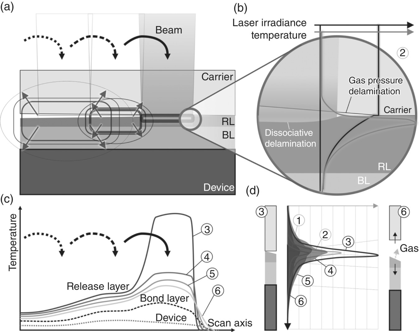
Figure 21.5 Schematic of the temperature evolution during UV DPSS laser debonding.
The smaller size of DPSS laser spots is beneficial for this debonding case, as the field size is of the same order of magnitude as the layer thicknesses. Therefore, heat diffusion occurs in all directions in space, and the in‐plane component reduces the temperature increase of the other layers considerably. Measurements have shown that this heating of the device surface is less than +30 °C owing to the fast heat dissipation into the surrounding regions. On the other hand, with large area exposure such as generated by excimer lasers, this 3D heat diffusion model is not applicable anymore. Caused by their large exposure area and low repetition rate, the generated heat can only diffuse orthogonally to the sample surface, as the perimeter of the debonding area is comparatively small. In other words, controlling the temperature impact is much easier in the small spot case. Large spots contrarily have the advantage of better homogeneity control within the exposure field and a relatively smaller border region as a source of inhomogeneity, although those stitching regions become more prominent than with the rather continuous small spot irregularities.
Concentrating the energy in time and space drastically improves efficiency, especially in thermal‐dominated materials like polyimides, and improves the debond speed to more than 1000 mm2 s−1 while covering large areas at lower laser energy. As a result, both throughput and thermal exposure of the sensitive components are positively affected, as are the overall costs of the system.
The debond gap does not open only because of the ablation process and the dissociative removal of material but also due to the conversion and heat‐induced gas pressure buildup, which can introduce local debond forces of variable strength that are given by the material’s chemical and physical properties and are controlled by laser settings such as pulse energy, spot size, spot overlap, and the timing. Again, the control of the laser parameters and their fine‐tuning to the material is crucial for a successful and homogenous delamination across the whole substrate due to a precisely defined debond force on a microscopic level. In practical terms, a successful and stable laser debond implies fine and precise management of the laser process parameters, continuous monitoring, and detailed and fast strategies to map out the process window that is individually tailored to the product requirements.
From an engineering perspective, the debond process is not always completed after the laser treatment. Depending on the postexposure behavior of the individual bond material and the quality of the treatment residual, no or some regained holding force has to be overcome to separate the carrier from the substrate. Yet again, the temporary bond material’s behavior and timing is decisive for successful completion. After separation, an optional removal of residue, cleaning of the substrate and the carrier with suitable solvents, is a quite common procedure, which has to be considered when choosing a particular material system.
In addition to maintaining exact control of the debonding process, the cost of debonding must be minimized. UV DPSS lasers for debonding feature a high pulse repetition frequency, which results in a high debonding throughput. Depending on the type of adhesive, required dose, and spot size, typical debonding can be achieved in less than one minute for 300 mm wafers. For panels, the debond time scales according to the panel size.
UV laser debonding is a universal debonding process that is applicable to a very wide range of devices, wafer types, and surfaces. It offers high process latitude and temperature stability to ease the integration of temporary carrier technology into the wafer production flow for stacked device applications. The high repetition frequency, low consumable costs, long lifetime and uptime, and high throughput of DPSS lasers with a small footprint of the source, coupled with precise and stable beam‐shaping optics, provide a reliable and efficient combination that enables debonding for cost‐sensitive advanced package types, such as FO‐WLP.
Acknowledgments
We would like to acknowledge Steffen Kröhnert, Jose Campos, Andrea Cardoso, Mariana Pires, Eoin O’Toole, and Raquel Pinto of NANIUM S.A. This work was partially carried out in the Enhanced Power Pilot Line (EPPL) project, funded by EU and national grants under the ENIAC program.
References
- 1 Brunnbauer, M., Meyer, I., Ofner, G. et al. (2008), Embedded wafer level ball grid array (eWLB). 33rd International Electronics Manufacturing Technology Conference 2008 (2008).
- 2 Jin, Y., Baraton, X., Yoon, S.W. et al. (2010). Next generation EWLB (embedded wafer level BGA) packaging. 12th Electronics Packaging Technology Conference (2010).
- 3 Jose Campos, A.C. (2015). Temporary wafer carrier solutions for thin FO‐WLP and eWLB‐based PoP. In: iWLPC (International Wafer Level Packaging Conference). San Jose, CA: SMTA International.
- 4 Lippert, T. (2009). UV laser ablation of polymers: from structuring to thin film deposition. In: Laser‐surface Interactions for New Materials Production (ed. A. Miotello and P.M. Ossi), 141–175. Berlin: Springer.
- 5 Andry, P., Budd, R., Polastre, R. et al. (2014). Advanced wafer bonding and laser debonding. IEEE 64th Electronic Components and Technology Conference (ECTC), Orlando, FL (S. 883–887).