Chapter 8
High-level Design Tools for Complex DSP Applications
Chapter Outline
High-level synthesis design methodology
LDPC decoder design example using PICO
Matrix multiplication design example using Catapult C
High-level synthesis design methodology
High level synthesis (HLS) [1], also known as behavioral synthesis and algorithmic synthesis, is a design process in which a high level, functional description of a design is automatically compiled into a RTL implementation that meets certain user specified design constraints. The HLS design description is ‘high level’ compared to RTL in two aspects: design abstraction, and specification language:
I. High level of abstraction: HLS input is an untimed (or partially timed) dataflow or computation specification of the design. This is higher level than RTL because it does not describe a specific cycle by cycle behavior and allows HLS tools the freedom to decide what to do in each clock cycle.
II. High level specification language: HLS input is specified in languages like C, C++, System C, or even Matlab, and allows use of advanced language features like loops, arrays, structs, classes, pointers, inheritance, overloading, template, polymorphism, etc. This is higher level than (synthesizable subset of) RTL description languages and allows concise, reusable, and readable design descriptions.
The objective of HLS is to extract parallelism from the input description, and construct a micro architecture that is faster and cheaper than simply executing the input description as a program on a microprocessor. The micro architecture contains a pipelined datapath and a cycle-by-cycle description of how data is routed through this datapath. The output of HLS may include:
I. RTL implementation: This includes the RTL netlist that contain the datapath, control logic, interfaces to I/O, host, and memories; as well as scripts, libraries, and synthesis timing constraints required to synthesize the RTL netlist using conventional logic synthesis flows.
II. Analysis feedback: This includes GUI and reports on performance bottlenecks, mapping of high level source code to RTL, hardware costs, etc, to help user understand and improve the micro architectures.
III. Verification Artifacts: This includes simulation test bench, linting checks, scripts, and library for code coverage, etc., to help user develop and debug high level language test suite and reuse these tests for RTL verification.
User specified constraints help HLS construct the desired micro architecture. These constraints include:
I. Target hardware: This includes the platform, technology library, clock frequency, etc, that the design is intended for. HLS uses this information to estimate sub-cycle timing and cost of the datapath.
II. Performance constraint: This may be expressed in the form of input sampling rate, output production rate, input-to-output latency, loop initiation intervals, loop latency, etc. These constraints impose cycle level timing constraints on the micro architecture.
III. Memory architecture: This specifies how multi-dimensional arrays are mapped to memories and memory interfaces, allowing HLS to construct micro architectures containing mult-port, multi-bank, arbitrated, external and internal memories.
IV. Interface constraint: This includes the protocol, ports, and handshake/arbitration logic to create at each input, output, host, and external memory interface. HLS generates these interface ports and logic in the RTL netlist so it can be easily integrated with other hardware blocks.
V. Design hierarchy: This partitions a design using hierarchy in the high level input description, allowing HLS to manage design complexity by divide-and-conquer.
HLS is not a substitute for a good RTL designer. For example, if the micro architecture is given, designing in RTL is easier and sufficient. HLS is designed for exploring different algorithms and architectures to find the best micro architecture under a variety of constraints. The primary benefits of HLS derive from its support for high level of abstraction and high level specification language:
I. Benefits of designing at a high level of abstraction:
a) Allows focus on designing core functionality, not implementation details. Easily explore different architectures.
b) Easily evaluate algorithmic changes.
c) Easily generate memory, IO, and host interfaces, as well as pipeline, stall, handshake and arbitration logic, etc.
d) Easily retarget for different hardware constraints or performance from the same input description.
II. Benefits of verifying at a high level of abstraction:
a) Easily debug and test functionality of input descriptions.
c) Test suite is reusable for RTL verification.
d) Code coverage and functional coverage is more meaningful and easier to achieve.
III. Benefits of high level specification language:
a) Legacy code can be reused for design and for verification.
b) Software development tools (e.g., Visual Studio) can be used.
c) Support advanced language features like polymorphism and templatized classes for concise, reusable input descriptions.
High-level design tools
To meet high performance and low power requirement of the VLSI digital signal processing system, traditional hardware design methods require designers to manually write the RTL codes which are too time-consuming for both designing and debugging.
Catapult C
Catapult C Synthesis [2] is an algorithmic synthesis tool that provides implementations from C++ working specifications. Catapult C Synthesis employs the industry standard ANSI C++ and System C to describe algorithms or functionality of the circuit. The output of Catapult C is a RTL netlist in either VHDL or Verilog HDL that can be synthesized to the gate level by using Precision RTL Synthesis, Design Compiler or similar RTL synthesis tools. Figure 8-1 shows the comparison between the traditional RTL design and Catapult C RTL design workflow.
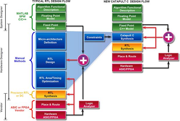
Figure 8-1: Catapult C Synthesis RTL design flow versus the traditional RTL design flow.
With this approach, full hierarchical systems comprised of both control blocks and algorithmic units are implemented. By speeding time to RTL and automating the generation of bug free RTL, the designer can significantly reduce the time to verified RTL. Catapult’s workflow provides modeling, synthesizing, and verifying complex ASICs and FPGAs allows hardware designers to explore micro-architecture and interface options. The designer should carefully tune architectural constraint parameters in the interactive environment to generate different micro architectures which can meet the design specifications.
The designers should start the Catapult C HLS design process from describing and simulating an algorithm. The algorithm description is written in pure ANSI C++ or SystemC source, describing only the functionality and data flows. Hardware requirements are not considered in this stage. The next step is to determine the target technology and architecture constraints. The target technology defines the building blocks in a design which can be ASIC or FPGA. Then the clock frequency and hardware constraints should be set. Hardware requirements such as parallelism and interface protocols can be set in Catapult through constraints, which, in turn, guide the synthesis process. Catapult C determines the micro-architecture of the generated RTL code based on the technology and clock frequency chosen by the designer. As depicted in Figure 8-2, with different technology settings, the architectures are different for the generated RTL codes even though the same clock frequency is chosen.
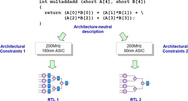
Figure 8-2: Target optimized RTL code generation.
Once the target technology and clock frequency are specified, the designer is free to begin exploring the design space using built-in HLS process. The designer can look at a wide range of alternatives, explore the trade-off between area and performance, and finally generate the hardware implementation which meets the design goals. Optimization methods including interface streaming, loop unrolling, loop merging and loop pipelining, and so on, can be selected by the designer to create a wide range of micro-architectures from the sequential to fully parallel implementations. However, the tool is not able to directly digest the design specification and automatically generate the desired hardware architecture. Therefore, the designer should still keep the big picture of the hardware architecture in mind and guide the tools to generate the optimized architecture by tuning the optimization options step by step.
Once all the steps described above are finished, an RTL module is generated based on the specification and optimization methods. The designer can use RTL verification tools to verify the correctness of the design. If there is anything that does not meet the requirements of the specification, the designer should go back to the Catapult C to modify the design.
A DSP system such as wireless communication signal processing system usually contains very complicated processing blocks which are developed and verified independently. Catapult C provides integration with many third-party tools which allow the designers to synthesize, simulate and verify the blocks for the DSP system. Figure 8-3 briefly shows one of the typical Catapult C tool flow for DPS system design.
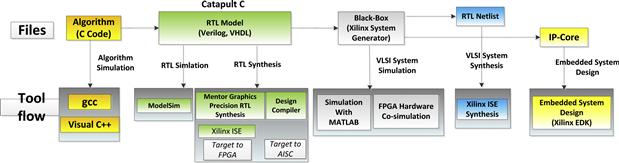
Figure 8-3: Catapult C HLS design tool flow.
During the algorithm development and simulation stage, the designer can write C++ program for fast algorithm development. The C++ program can be compiled using Microsoft Visual C++ or GCC compiler and Catapult C IDE has provided the interface with these compilers. By using bit-accurate arithmetic library (for example, AC data types), the fixed-point algorithm simulation can be done by converting the floating-point C++ model. Afterwards, Catapult C generates the RTL model according to the architecture constraints provided by the designer. The designer can employ ModelSim to simulate and verify the functionality of the RTL model or directly synthesize these RTL model by Precision RTL (for FPGA), Xilinx ISE (for FPGA) or Design Compiler (for ASIC). The designer can also generate a bigger system with the RTL model generated by Catapult C and blocks generated by other tools such as Xilinx System Generator and Xilinx EDK and so on.
PICO
The PICO C-Synthesis [3, 4] creates application accelerators from un-timed C for complex processing hardware in video, audio, imaging, wireless, and encryption domains. Figure 8-4 shows the overall design flow for creating application accelerators using PICO. The user provides an algorithm in C along with functional test inputs and design constraints such as the target throughput, clock frequency, and technology library. The PICO system automatically generates the synthesizable RTL, customized test benches, and System C models at various levels of accuracy as well as synthesis and simulation scripts. PICO is based on an advanced parallelizing compiler that finds and exploits the parallelism at all levels in the C code. The quality of the generated RTL is competitive with manual design, and the RTL is guaranteed to be functionally equivalent to the algorithmic C input description. The generated RTL can then be taken through standard simulation, synthesis, place, and route tools and integrated into the SoC through automatically configured scripts.
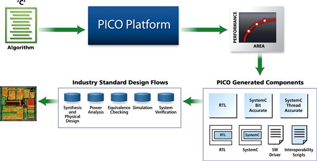
Figure 8-4: System level design flow using PICO.
Figure 8-5 shows the general structure of hardware generated by PICO from a high level C procedure. This architecture template is called a pipeline of processing arrays (PPA). Using this architecture template, the PICO compiler will map each loop in the top level C procedure to a hardware block or a processing array (PA). PAs communicate with each other via FIFOs, memories, or raw signals. A timing controller is used to schedule the pipeline, and to preserve the sequential semantics of the original C procedure. The host interface and the task frame memory were used to provide the integration of the PPA hardware into a system using memory mapped IO.
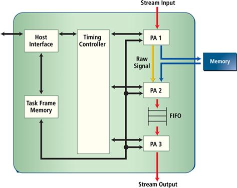
Figure 8-5: The PPA architecture template.
System Generator
System Generator [5] is a system-level DSP design tool from Xilinx. It uses the Simulink design environment for FPGA design, which is very suitable for hardware design. Designs are implemented by using modules from Xilinx blockset. Many modules are provided for Simulink, from common building blocks such as adders, multipliers, and registers to complex building blocks such as forward error correction blocks, FFTs, filters, and memories. These blocks make the design process much easy and deliver optimized results for the selected device. Furthermore, all of the FPGA implementation steps including synthesis and place and route are automatically performed to generate an FPGA programming file.
The design flow of using System Generator is described below. Usually, design starts from algorithm exploration. System Generator is very useful for algorithm exploration, design prototyping, and model analysis. With System Generator, we can fast model the problem and different algorithms. We not only can model the algorithm by using Xilinx blockset, but also can integrate the Simulink blocks and MATLAB M-code into the System Generator. After we model the algorithm, we can simulate their performance and estimate hardware cost in System Generator. With the help of these comparison results, we can make a fast and proper choice of the algorithm.
To speed up the simulation, System Generator provides hardware co-simulation. This makes it possible to incorporate a design running in an FPGA directly into a Simulink simulation. In this way, part of the design is running on FPGA and part of the design is running in Simulink. This is particularly useful when portions of a design need to be verified but need a lot of time when doing pure software simulation.
After we choose the algorithm, we can begin to implement the design part by part. In this level, we can use Xilinx blockset to do the implementation. System Generator provides various Xilinx blockset, from basic ones to complex ones. We also can implement the design in HDL and use an HDL wrapper to make it a component in System Generator. There are many parameters inside each module. We can refer Matlab variable in the parameters. When we want to change the parameter, we just need to assign a different value in Matlab. This makes the design very flexible and easy to maintain.
When we have designed all the modules, we can integrate them together into a whole system. We also can integrate a Matlab testbench to the system. By inputting Matlab variables to the design, we can design much complicated verification method in a short time. If there the design is all correct, we can generate the netlist to the ISE to the specific FPGA. Then you can synthesize the design in ISE and download to FPGA.
Case studies
In the following case studies, we will present three complex DSP accelerator designs using high-level design tools: 1) LDPC decoder accelerator design using PICO C; 2) Matrix multiplication accelerator design using Catapult C; and 3) QR decomposition accelerator design using System Generator.
LDPC decoder design example using PICO
Low-density parity-check (LDPC) codes [6] have received tremendous attention in the coding community because of their excellent error correction capability and near-capacity performance. Some randomly constructed LDPC codes, measured in Bit Error Rate (BER), come very close to the Shannon limit for the AWGN channel with iterative decoding and very long block sizes (on the order of 106 to 107). The remarkable error correction capabilities of LDPC codes have led to their recent adoption in many standards, such as IEEE 802.11n, IEEE 802.16e, and IEEE 802.15.3c.
As wireless standards are rapidly changing and different wireless standards employ different types of LDPC codes, it is very important to design a flexible and scalable LDPC decoder that can be tailored to different wireless applications. In this section, we will explore the design space of efficient implementations of LDPC decoders using the PICO high level synthesis methodology. Under the guidance of the designers, PICO can effectively exploit the parallelism of a given algorithm, and then create an area-time-power efficient hardware architecture for the algorithm. We will present a partial-parallel LDPC decoder implementation using PICO.
A binary LDPC code is a linear block code specified by a very sparse binary M by N parity check matrix:
H·xT = 0,
where x is a codeword and H can be viewed as a bipartite graph where each column and row in H represents a variable node and a check node, respectively. Each element of the parity check matrix is either a zero or a one, where nonzero entries are typically placed at random to achieve good performance. During the encoding process, N-K redundant bits are added to the K information bits to create a codeword length of N bits. The code rate is the ratio of the information bits to the total bits in a codeword. LDPC codes are often represented by a bi-partite graph called a Tanner graph. There are two types of nodes in a Tanner graph, variable nodes and check nodes. A variable node corresponds to a coded bit or a column of the parity check matrix, and a check node corresponds to a parity check equation or a row of the parity check matrix. There is an edge between each pair of nodes if there is a one in the corresponding parity check matrix entry. The number of nonzero elements in each row or column of a parity check matrix is called the degree of that node. An LDPC code is regular or irregular based on the node degrees. If variable or check nodes have different degrees, then the LDPC code is called irregular, otherwise, it is called regular. Generally, irregular codes have better performance than regular codes. On the other hand, irregularity of the code will result in more complex hardware architecture.
Non-zero elements in H are typically placed at random positions to achieve good coding performance. However, this randomness is unfavorable for efficient VLSI implementation that calls for structured design. To address this issue, block-structured quasi-cyclic LDPC codes are recently proposed for several new communication standards such as IEEE 802.11n, IEEE 802.16e, and DVB-S2. As shown in Figure 8-6, the parity check matrix can be viewed as a 2-D array of square sub matrices. Each sub matrix is either a zero matrix or a cyclically shifted identity matrix Ix. Generally, the block-structured parity check matrix H consists of a j-by-k array of z-by-z cyclically shifted identity matrices with random shift values x (0 = < x < = z).
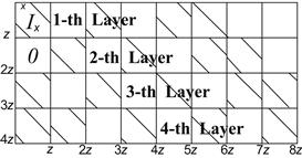
Figure 8-6: A block structured parity check matrix with block rows (or layers) j = 4 and block columns k = 8, where the sub-matrix size is z-by-z.
A good tradeoff between design complexity and decoding throughput is partially parallel decoding by grouping a certain number of variable and check nodes into a cluster for parallel processing. Furthermore, the layered decoding algorithm [7] can be applied to improve the decoding convergence time by a factor of two and hence increases the throughput by two times.
In a block-structured parity-check matrix, which is a j by k array of z by z sub-matrices, each sub-matrix is either a zero or a shifted identity matrix with random shift value. In every layer, each column has at most one 1, which satisfies that there are no data dependencies between the variable node messages, so that the messages flow in tandem only between the adjacent layers. The block size z is variable corresponding to the code definition in the standards.
To simplify the hardware implementation, the scaled min-sum algorithm [8] is used. This algorithm is summarized as follows. Let Qmn denote the variable node log likelihood ratio (LLR) message sent from variable node n to the check node m, Rmn denote the check node LLR message sent from the check node m to the variable node n, and APPn denote the a posteriori probability ratio (APP) for variable node n, then:
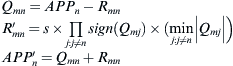
where s is a scaling factor. The APP messages are initialized with the channel reliability values of the coded bits.
Hard decisions can be made after every horizontal layer based on the sign of APPn. If all parity-check equations are satisfied or the pre-determined maximum number of iterations is reached, then the decoding algorithm stops. Otherwise, the algorithm repeats for the next horizontal layer.
To implement this algorithm in hardware, we use a block-serial decoding method [9]: data in each layer is processed block-column by block-column. The decoder first reads APP and R messages from memory, calculates Q, and then finds the minimum and the second minimum values for each row m over all column n. Then, the decoder computes the new R and APP values based on the two minimum values, and writes the new R and APP values back to memory. The algorithm is coded in an un-timed C code. A section of the C code is shown in Figure 8-7, which depicts the PPA architecture generated by the PICO C compiler. The parallelism of this architecture is at the level of the sub-matrix size z. Note that the ‘pragma unroll’ statement in the C code will be used by the PICO C compiler to determine the parallelism level. Multiple instances of the decoding cores are generated by the PICO C compiler to achieve a large decoder parallelism.
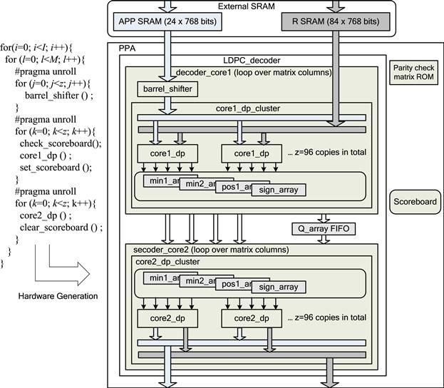
Figure 8-7: Pipelined LDPC decoder architecture generated by PICO.
As a case study, a flexible LDPC decoder which fully supports the IEEE 802.16e standard was described in an un-timed C procedure, and then the PICO software was used to create synthesizable RTLs. The generated RTLs were synthesized using Synopsys Design Compiler, and placed & routed using Cadence SoC Encounter on a TSMC 65nm 0.9V 8-metal layer CMOS technology. Table 8-1 summarizes the main features of this decoder.
Table 8-1: ASIC synthesis result.
| Core area | 1.2 mm2 |
| Clock frequency | 400 MHz |
| Power consumption | 180 mW |
| Maximum throughput | 415 Mbps |
| Maximum latency | 2.8 μs |
Compared to the manual RTL designs [10, 11] which usually took 6 months to finish, the C based design using PICO technology only took 2 weeks to complete, and is able to achieve high performance in terms of area, power, and throughput. The area overhead is about 15% compared to the manual LDPC decoders [10, 11] that we have implemented before at Rice University.
Matrix multiplication design example using Catapult C
In this section, we will take matrix multiplication as an example and use Catapult C to explore the design space to achieve different design goals. Matrix multiplication is a very important computation block for many signal processing applications, such as MIMO detection in wireless communication, multimedia encoding/decoding, and so on.
The computational complexity for an N × N matrix multiplication is O(N3). Usually parallel architecture is employed to accelerate the matrix multiplication computations. According to different design requirements, different parallel architectures can be utilized and there is trade-off between the throughput performance and hardware cost. By using interactive GUI of Catapult C, we can explorer different the micro-architectures and generate the RTL models.
Assume A and B are two matrices, compute C = A × B. The problem is depicted in Figure 8-8, in which we can see the result matrix C has the same width as matrix B, while its height is equal to the width of matrix A. The C code for the matrix multiplication is listed below. To make the problem easy to describe, we assume A and B are both 4 × 4 matrices.
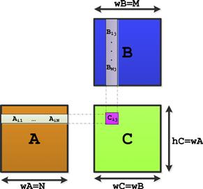
Figure 8-8: Matrix multiplication.
#define NUM 4
void Matrix_multiplication(int A[NUM][NUM], int B[NUM][NUM], int C[NUM][NUM])
{
for(int i = 0; i<NUM; i++)
{
for(int j = 0; j < NUM; j++)
{
C[i][j] = 0;
for(int k = 0; k < NUM; k++)
{
C[i][j]+ = A[i][k] ∗ B[k][j];
}
}
}
}
Checking the code carefully, we notice that the main body of the function is a three-level nested for loop. Since the multiplication computations are operated on different sets of data, there are neither data dependencies nor data races. For instance the computations for each Cij can be run in parallel as long as there are enough computation units. To compute Cij, a dot product with a row of matrix A and a column of matrix B is performed, in which all the multiplications can be executed in parallel. There are many parameters we can explore in the design space to parallelize the matrix multiplication. If we check this function again from a hardware designer’s perspective, we can regard this function as a description of a hardware model. The loops inside the function correspond to the pipeline structure in the hardware architecture. Since the main part of the function is a three-level nested for loop, we should focus more on the loop optimization to get high performance. In addition, we notice the input and output interfaces of this function are two-dimension arrays which represent memory in the hardware.
First, we convert the code to fixed-point version, and add the necessary compiling pragma according to Catapult C specification. In this program, we define the data type of the elements in matrix A and B as int16 (16-bit integer), which has been defined in ac_int.h. For C, int34 is used to avoid overflow. We do a software simulation using the fixed-point C program and verify the results.
#define NUM 4
#include ‘ac_int.h’
#pragma hls_design top
void Matrix_multiplication(int16 A[NUM][NUM], int16 B[NUM][NUM], int C34[NUM][NUM])
{
OUTERLOOP: for(int i = 0; i<NUM; i++)
{
INNERLOOP: for(int j = 0; j < NUM; j++)
{
C[i][j] = 0;
RESULTLOOP: for(int k = 0; k < NUM; k++)
{
C[i][j] + = A[i][k] ∗ B[k][j];
}
}
}
}
To begin the design with Catapult C, we set up the basic technology configurations. In this example, we select Xilinx Virtex-II Pro FPGA chip as the technology target, and set the design frequency to 100 MHz. For the interface setting, we use the default configurations, which include a clock and a synchronous reset signal. We also keep the default configurations for the architectural constraints. We set area as our design goal and try to minimize the area of the logic core. Figure 8-9 shows the generated Gantt chart of this design. From the Gantt chart, it is clear that Catapult C generates a serial implementation. In this serial implementation, the circuit reads two data from the memory and computes the multiplication product in the first clock cycle. Then the circuit performs an addition operation in the second clock cycle. The logic repeats the same operations until the computations are finished.
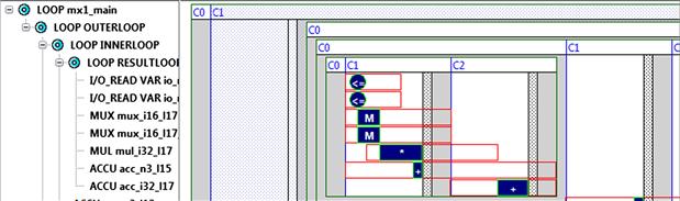
Figure 8-9: Gantt chart for design with the default configuration.
By pipelining the loops, we are able to hide some execution latency to increase the throughput. We can decide at which level the loop should be pipelined and we can change the setting for each loop separated. In Catapult C, it is still necessary for the designer to keep in mind the low-level details of the hardware, so that he can take advantage of loop pipelining by carefully applying the right loop optimization techniques to the right loops.
Next, we further optimize the implementation by using loop unrolling and loop merging techniques. By enabling loop unrolling, we increase the hardware parallelism to trade higher throughput. For example, we can unroll the INNERLOOP and RESULTLOOP. Since these loops are executed for 16 times, the generated hardware uses 16 multipliers after loop unrolling. The Gantt chart of the loop unrolling result is shown in Figure 8-10. As we have expected, sixteen multipliers are employed and running in parallel.
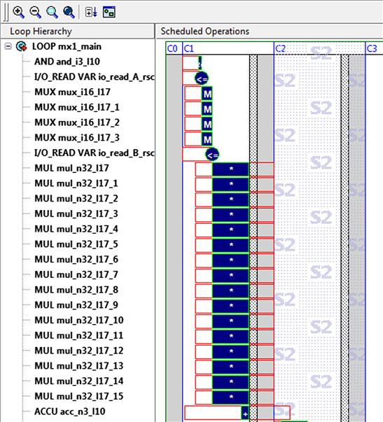
Figure 8-10: Gantt chart for loop unrolling.
So far, we only changed the loop optimization settings. It is also possible to change the interface to meet the design specification and the design goal. In the previous design, matrices A, B, and C are all represented by two dimension arrays and they are mapped to memory inside the chip. For example, both A and B are mapped to 1 × 256 bits memory (4 × 4 × 16 bits). By default, Catapult C assumes all of the data should be written into the memory before performing all the computations. In the real world application, such as signal processing for wireless communications and multimedia processing, the data are streamed into the circuit instead of the coming in blocks. Therefore, in the next step, we try to change the interface options to make the matrix multiplication block support streaming data I/O.
By setting the streaming options to 1, we are trying to extract one of the matrix’s dimension and stream this dimension’s data into the circuit. For example, to input matrix A (defined as: int A[4][4]), we input four successive vectors (A[0], A[1], A[2], A[3]) in order. By changing the streaming setting to 1, the interface for A and B now becomes 1 × 64 bits memory.
So far, we have explored several optimization techniques. Table 8-2 shows the performance comparison designs with different design parameters. Since we only care about the latency and area, only these two terms are listed. Table 8-2 shows the performance comparison.
Table 8-2: Performance comparison for different optimizations.
| Latency Cycles | Total Area | |
| Default | 159 | 1314 |
| Pipelining | 65 | 1995 |
| Loop unrolling | 5 | 9235 |
| Streaming with partial loop unrolling | 17 | 2293 |
From the table, we can see by using the pipelining and loop unrolling techniques, the latency cycles are reduced significantly from 159 to 5 while the cost of area increases from 1314 to 9235. By using the streaming I/O and partial loop unrolling, we found a sweet point between latency and area, which shows a small latency of 17 cycles and a relatively small area 2293.
QR decomposition design example using System Generator
In this section, we will design a 4x4 QR decomposition hardware accelerator by using the System Generator. The accelerator decomposes a 4x4 matrix ![]() into two 4x4 matrixes
into two 4x4 matrixes ![]() and
and ![]() where
where ![]() is a unitary matrix and
is a unitary matrix and ![]() is an upper triangle matrix. Nowadays, QR decomposition is wildly used. For example if we want to solve a matrix equation
is an upper triangle matrix. Nowadays, QR decomposition is wildly used. For example if we want to solve a matrix equation ![]() , we can decompose
, we can decompose ![]() into
into ![]() and
and ![]() . Then the equation becomes
. Then the equation becomes ![]() . Now we can move
. Now we can move ![]() to the other side of the equation. The equation becomes
to the other side of the equation. The equation becomes ![]() .
. ![]() is the conjugate transpose of
is the conjugate transpose of ![]() , which is equal to
, which is equal to ![]() . Because now
. Because now ![]() is an upper triangle matrix, we can do back substitution to figure out
is an upper triangle matrix, we can do back substitution to figure out ![]() .
.
Many methods are proposed to perform QR decomposition. Here we will focus on Givens rotation. The idea of Givens rotation is to rotate the current vector with an angle, which makes part of the current vector become 0. It is shown below:
![]()
and
![]()
![]()
![]()
By repeatedly applying Givens rotation to matrix ![]() , we can decompose it into
, we can decompose it into ![]() and
and ![]() .
.
The system architecture is shown in Figure 8-11. The light gray node is delay node. It delays the input data one cycle. The dark gray node is processing node. It has two modes: vectoring and rotating. In the vectoring mode, the horizontal output is the magnitude of the input vector and the vertical output is 0, and the angle of the vector is stored inside the node. In the rotating mode, the stored angle is used to rotate the input vector. The horizontal output is the rotated value of the input X, and the vertical output is the rotated value of the input Y. Only the first time the processing node receives the data of the matrix, the node will operate in the vectoring mode. In other time, the processing node works in the rotating mode. For example, when A11 and A21 arrive at the upper left processing node, the node operates in the vectoring mode. The angle between A11 and A21 is stored inside the node. When the next set of data A12 and A22 arrives at that processing node, the node works in the rotating mode to rotate the A12 and A22 by using the stored angle. And the node will continue working in the rotating mode until the next matrix. By connecting the delay nodes and the processing nodes in the following way, the system can decompose a 4x4 matrix. When inputting a data matrix ![]() and an identity matrix
and an identity matrix ![]() , the output will be matrixes
, the output will be matrixes ![]() and
and ![]() .
.

Figure 8-11: System architecture.
After we choose the algorithm and architecture, we can begin to do the implementation by using the Xilinx Blockset and Xilinx Reference Blockset from the Simulink library. These libraries will appear in Simulink after we install the System Generator.
First, we need to implement the processing node. As we know, processing node has two modes. For the vectoring mode, CORDIC ATAN is used. The module is in Xilinx Reference Blockset/Math. The module has two inputs: X and Y. They represent a vector. The module also has two outputs. MAG is the magnitude of the input vector, and ATAN is the angle of the vector. As stated in its document, the MAG needs to be compensated by 1/1.646760 after outputting. This is implemented by a CMULT at the magnitude output of the CORDIC ATAN, as shown in Figure 8-12. CMULT is in Xilinx Blockset/Math. For the rotating mode, CORDIC SINCOS is used. The module has three inputs. THETA is the angle used for rotating. X and Y represent a vector. According to the document, two inputs X and Y need to be compensated by 1/1.646760 before inputting to the module. CMULT is used to compensate both. Two outputs, COS and SIN, are the ROTATED_X and ROTATED_Y, respectively.
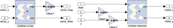
Figure 8-12: Implementation of vectoring and rotating.
After we implement both vectoring and rotating modules, we can use them to implement the processing node. This is shown in Figure 8-13. The processing node has four inputs. X and Y represent the vector. They are connected to the vectoring and rotating modules. MODE controls if the processing node works in the vectoring mode or the rotating mode. OUT_EN is the enable signal for the output. Register is connected between the vectoring module and the rotating module. It keeps the angle calculated from the vectoring module. Register can be found from Xilinx Blockset/Memory. The processing node has four outputs. OUT_X and OUT_Y represent output vector. Muxes from Xilinx Blockset/Control Logic control which value sent to OUT_X and OUT_Y. In vectoring mode, the processing node will output the magnitude of the X and Y to OUT_X and 0 to OUT_Y. Zero is implemented by Constant from Xilinx Blockset/Basic Elements. In rotating mode, the processing node will output the ROTATED_X to the OUT_X and the ROTATED_Y to OUT_Y. MODE_TO_NEXT and OUT_EN_NEXT are the control signals sent to the next processing mode. They are just the delayed version the MODE and OUT_EN signals. The delay is 15. This is because vectoring or rotating needs 14 cycles and Mux needs 1 cycle.
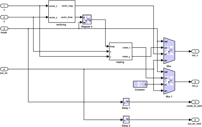
Figure 8-13: Implementation of processing node.
Now we can connect processing node to each other to implement the system as shown in Figure 8-14. Delay node is implemented by Register with specified delay. In this implementation, the delay is set to 15, because each processing node will consume 15 cycles to output a data. The OUT_X of the processing node is connected to the next horizontal node. The OUT_Y of the processing node is connected to the next vertical node. The whole system has six inputs. A1, A2, A3, and A4 are input data. MODE is control signal and DATA_EN_I is input data enable signal. It also has five outputs. R1, R2, R3, and R4 are output data and DATA_EN_O represent when the output data is available. A few Up Sample and Down Sample are used in the system. This is because each processing node needs 15 cycles to output the data, but there will a new input data in each cycle. By using the Up Sample and Down Sample, the system creates a new clock domain, which is 15 times faster than the main clock.
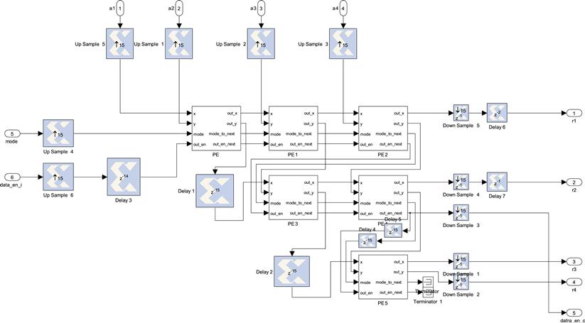
Figure 8-14: Top level block diagram for the QR decomposition system.
Conclusion
As the demand for high performance DSP systems is rapidly increasing, the chip designer faces the challenge of implementing complex algorithms quickly and efficiently without compromising on power consumption. High level synthesis, which can automatically create efficient hardware from an untimed C algorithm, can provide the solution. With the high level design tools, the designers work at a higher level of abstraction, starting with an algorithmic description in a high-level language such as ANSI C/C++ and System C.
In this chapter, we have introduced the basic methodology of the high level design tools for DSP systems and summarized some important features of the high level synthesis design flow. We have introduced several high level synthesis tools for ASIC/FPGA implementation of the complex DSP systems. In the case studies, we gave three DSP design examples using high level design tools. The design created from high level design tools is comparable to a manual hand design in terms of area-power-timing but with a much faster design cycle.
Today, there are several very successful high level synthesis tools that provide effective solutions in building complex DSP systems. The high level design tools for DSP systems have great potentials to be widely used in the DSP designers’ community.
REFERENCES
1. Coussy P, Morawiec A. High-Level Synthesis rom Algorithm to Digital Circuit. Netherlands: Springer; 2008.
2. Catapult C. Synthesis official website. In: http://www.mentor.com/esl/catapult.
3. Synfora PICO Product. In: http://www.synfora.com.
4. Xilinx System Generator Product. In: http://www.xilinx.com/tools/sysgen.htm.
5. Aditya S, Kathail V. Algorithmic Synthesis Using PICO. Springer Netherlands 2008;53–74.
6. Gallager R. Low-density parity-check codes. IEEE Transaction on Information Theory. Jan 1962;vol. 8:21–28.
7. Hocevar DE. A reduced complexity decoder architecture via layered decoding of LDPC codes. In: IEEE Workshop on Signal Processing Systems. SIPS 2004;107–112.
8. Chen J, Dholakia A, Eleftheriou E, Fossorier M, Hu X. Reduced-complexity decoding of LDPC codes. IEEE Transactions on Communications. 2005;vol. 53 pp. 1288–1299.
9. Sun Y, Cavallaro JR. A low-power 1-Gbps reconfigurable LDPC decoder design for multiple 4G wireless standards. In: IEEE International SOC Conference. SoCC Sept. 2008;367–370.
10. Sun Y, Karkooti M, Cavallaro JR. High throughput, parallel, scalable LDPC encoder/decoder architecture for OFDM systems. In: 2006 IEEE Dallas/CAS Workshop on Design, Applications, Integration and Software. Oct. 2006;39–42.
11. Sun Y, Karkooti M, Cavallaro JR. VLSI decoder architecture for high throughput, variable block-size and multi-rate LDPC codes. In: IEEE International Symposium on Circuits and Systems. ISCAS May 2007.