
3
DATA ACQUISITION METHODS FOR MULTICHANNEL SENSOR SYSTEMS
Technological and manufacturing processes are sources of the initial data for multichannel sensor systems. The data are received by a control system as random processes of parameter variations and in the form of random events.
Multichannel data acquisition systems are intended for the transformation of the initial parameters of processes and events (output signals from one or several sensors and transducers) into equivalent digital signals, suitable for further processing, transferring and input into a central computer, which controls the channeling data acquisition and forms data arrays for further display or its use in control systems. Modern data acquisition systems are able to handle practically all physical and chemical quantities, due to the wide variety of frequency–time-domain sensors and transducers.
Methods of data acquisition depend on solved tasks of control and measurement and directly influence the structure and functionalities of multichannel data acquisition systems.
A modern measurement and control sensor system could be set up in different ways. A central computer is connected to a number of input (sensors) and output (actuators) devices. In such systems, many frequency–time-domain sensors pick up information about process-related measurands.
Two traditional methods of data acquisition are widely used in modern automatic control and measuring systems. These are:
- Methods using time-division channelling, based on multiplexing sensors, i.e. on time-shared data acquisition from each sensor.
- Methods using space-division channelling, based on simultaneous data acquisition from all the sensors.
In both cases, the constancy of data sources, i.e. access to information at any time dependent on solved control and measuring tasks, is used.
3.1 Data Acquisition Method with Time-Division Channelling
The most frequently used configuration of a data acquisition system with time-division channelling (multiplexing) is shown in Figure 3.1.
In this system outputs of the frequency sensors f1, f2, … fn are connected to the frequency-to-code converter F/# in turn with the help of the digital multiplexer MX, which is controlled by the microcontroller μK. The frequency-to-code converter converts the frequency fx to a binary code, for example, according to the direct counting method by counting Tx = 1/fx periods during the gate time Tq (quantization time) or according to the indirect counting method by counting impulses of the high reference frequency f0 during one Tx or nTx periods. In modern data acquisition systems for frequency output sensors, the frequency-to-code conversion can be realized directly by microcontrollers without any additional hardware.
After the frequency-to-code conversion, the binary code enters the microcontroller to form data arrays. If necessary, additional signal processing, for example, linearization, unification, scaling, etc. can be realized in the microcontroller or DSP. The data is then input into a central computer (through one of the system buses, I/O ports or with the help of direct memory access (DMA)) for further processing, display or use in the control system.
Sensor polling can be cyclic synchronous as well as software-controlled asynchronous–the microcontroller chooses the required sensors depending on the task. In data acquisition systems of data with frequency conversion at cyclic polling with constant time intervals between identical operations the cycle polling time τ0 can be calculated according to the following equation:
where:
— Tq is the quantization time in the frequency-to-code converter.
— τdelay1 is the time delay between the ending of the conversion in the previous sensor and the command to poll the next sensor.
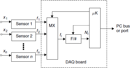
Figure 3.1 A Data acquisition system with time-division channelling
— τdelay2 is the time delay of the frequency conversion starting after the sensor connection.
— n is the number of sensors in the multichannel data acquisition system.
Values of the time intervals and delays are determined by methods of the measurement of informative parameters, methods of separation and electronic components used. At the preset values Tq, τdelay1, τdelay2 and the cycle polling time τ0 can be changed only by changing n.
The constant sequence of sensor polling and the cyclicity, controlled by the micro-controller, is the reason for information losses. In order to reduce these losses, it is necessary to either increase the frequency of sensor polling or to use other technological and algorithmic measures.
The multichannel device for data acquisition based on the method of accelerated polling for period output sensors is shown in Figure 3.2. It simultaneously forms the period duration Tx and the sensor's number in its output [87]. The device contains some RS-triggers (according to the number of channels in the system) with multiport elements AND, which works similar to a frequency switch, and a coder CD for conversion of the input positional code to the binary code of channel's number. In this device, signals from periodic output sensors arrive to synchronous inputs of D-triggers of register 1. The coder's output and the output of the first multiport element AND 4 form the device's output. The synchronous inputs of D-triggers and the S-input of RS-triggers are dynamic inputs which toggle from a positive logic swing, other inputs are potential.
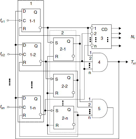
Figure 3.2 Device for data acquisition based on the method of accelerated polling for periodic output sensors
The device works as follows. At the beginning of each cycle all triggers of both registers are in the logical state ‘0’. In some moment of time the D-trigger connected to the ith channel is toggled to ‘1’ by the positive logic swing. From the inverse output of this trigger, logic ‘0’ arrives at the i-th input of the multiport logic element AND 4, the S-input of RS-trigger 2 and the ith input of the coder where it will be converted to the binary code of channel's number. The logic level ‘0’ of multiport logic element AND 4 forbids toggles of all other D-triggers of the register ‘1’ until the next positive logic swing in this channel. At this logical level the D-trigger in the ith channel is toggled to ‘0’. The RS-trigger in the same channel is also toggled. This trigger locks the D-trigger at R-input by the positive logic swing on the inverse output up to the cycle ending. Thus, the logical ‘0’ output of the multiport element AND 4 and the binary code of the chosen channel's number on the coder's output remain constant during the pulse propagation in this channel.
The next toggled trigger will be the D-trigger of that channel, the C-input of which will then act as the logic swing before all others and all described actions will repeat again. After the toggle ‘1’ of the RS-triggers of all n channels, the second multiport element AND 5 will toggle and reset the register based on RS-triggers to the ‘0’ level.
This device has extended functionalities, due to the formation of the time Txi of the multichannel period-to-code converter. The polling of all measuring channels is realized during one cycle. Moreover it is carried out with high speed because the next measuring channel is chosen according to the nearest logic swing from all the nonselected channels.
A similar method of accelerated polling for quasi-digital sensors was also used in multichannel digital frequency selector design [88]. The distinctive feature of these frequency selectors is the increased polling frequency for channels with higher input frequencies that has allowed reduction of the dynamic error of measurement in this channel.
The original data acquisition method for multichannel frequency-to-code converters which reduce information losses in multichannel data acquisition systems by timeshared polling of frequency output sensors is described in [89]. The method consists of a choice of measuring channels with the nearest pulses on the phase of converted frequencies; the separation of the number of channels, which can be simultaneously served by the counter; storing the number of these channels in memory; the connection of the chosen channels to the counter's input and the frequency-to-code conversion in them.
Further, the numbers of channels are stored, in which repeatedly there was no code of converted frequencies at the moment of arrival of the challenging signal from the outside, and applied extraordinarily their connection to the counter's output with arrival to these channels of the nearest pulses on time. Then the number of channels in which measurement of time intervals is supposed will be stored, and uses its extraordinary connection to the counter's input when the start pulses arrive, so beginning the time measurement.
This method of data acquisition allows minimum information losses because of nonsyncronism and nonphasing converted and polling frequencies. This arises because of the channels' sequence of connection to the counter's input results in the increased probability of the next pulses of converted frequencies occurring at once after the ending of the count in previous channels, as the sample is carried out from all sets of converter channels.
Thus, channel choice is determined as a result of a comparison of information in all the channels by revealing the first pulse of one of channels from which the control pulses are forming for processing units.
Data acquisition with time-division channelling allows inexpensive multichannel data acquisition systems for quasi-digital sensors.
3.2 Data Acquisition Method with Space-Division Channelling
The most frequently used configuration of a data acquisition system with space-division channelling is shown in Figure 3.3.
In such a system instead of one frequency-to-code converter and an n-channel multiplexer, n frequency-to-code converters (according to the number of channels) and a microprocessor system with n inputs are used. That is, for simultaneous measurement of several frequencies, there is an independent channel for the frequency-to-code converter. The microprocessor simultaneously starts all converters (continuous periodic synchronously or software-controlled asynchronously), and at the end of the measurement processes reads results. It is possible to make some realizations of the frequency-to-code converter—the microprocessor interface: by polling, interrupt or DMA. Due to n independently working measuring channels (the sensor—the frequency-to-code converter—the microprocessor's input), n conversions are realized simultaneously. It increases the system productivity and speed by n times which is determined by the time Tq + treadout. However, this important advantage—the reduction of measuring information losses—is achieved by additional hardware and cost. All this limits the number of channels in a data acquisition system or requires the use of special technical measures, for example, the separation of some element from the converter, which can be common for all frequency-to-code converters, etc.
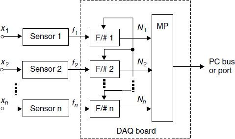
Figure 3.3 Data acquisition system with space-division channelling
One such solution is used in a device for multichannel frequency conversion [90]. Simultaneously with hardware reduction and parallel measurement of all sensor frequencies, accuracy is increased without increasing time of measurement, due to the elimination of the influence of sensor frequency fluctuations. The circuit of such a device for simultaneous conversion of frequencies f1, f2, … fn, is shown in Figure 3.4. Each channel contains a frequency divider, a switch and a buffer register. The counter of the reference frequency f0, and the register are common for all measuring channels.
Let's consider how this device works in detail. For measurement of any input frequency the microprocessor generates a command, which regulates the divider overflow pulse propagation through switches to the buffer registers. The first overflow pulse from the divider starts the ‘calibration’. This pulse puts the logic ‘1’ in the appropriate register's bit and copies the counter's content into the buffer register. Simultaneously, the overflow pulse propagation for writing is forbidden until the new command from the microcontroller. During the frequency measurement, information from the buffer register is readout by the microprocessor at the necessary moment of time. After the reading this register will be nulled. The information from the register about divider overflow and the counter of reference frequency is readout by the microprocessor periodically with a greater frequency, than the frequency of overflow pulses. The overflow pulse frequency is determined by the counter capacity and the frequency of pulses to its input. It excludes pulse losses. At the end of the measurement cycle of frequency, a command similar to the command at the beginning of the cycle is generated by switches. The next divider overflow pulse after this command determines the end of a measurement cycle. It writes the information from the reference frequency counter into the buffer register for further readout by the microprocessor.
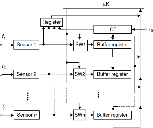
Figure 3.4 Device for simultaneous multichannel frequency conversion
Thus, the following information enters the microprocessor during frequency conversion:
— K1 is the number of divider overflows.
— K0 is the number of reference frequency counter overflows.
— n1 is the number written into the reference frequency counter at the beginning of the measurement cycle.
— n2 is the number written into the reference frequency counter at the end of the measurement cycle.
The converted frequency can be calculated according to the following equation:
where f0 is the reference frequency; f1 is the input frequency (measurand); N1 is the divider capacity; N0 is the reference frequency counter capacity.
The device for frequency measurements receives some measurement results during one cycle. The frequency for each measurement is determined by these results and the received results are averaged. It reduces the measurement error from pulses fluctuations. Thus, the measurement cycle duration is constant.
During simultaneous measurement of several frequencies the dividers' overflow pulses enter the appropriate bits of the register. The reading of information from buffer registers is separated in time. Hence, measuring frequency channels do not influence each other.
The method of data acquisition for quasi-digital sensors with space-division channelling is becoming increasingly attractive due to the small cost of frequency-to-code converters. A separate frequency-to-code converter for each channel allows a much higher polling frequency for each channel.
3.3 Smart Sensor Architectures and Data Acquisition
Depending on the smart sensor architecture, various data acquisition schemes are possible. Let us consider some of them. In the smart sensor architecture shown in Figure 3.5, the analog output of the sensor element S is at first amplified and corrected for offset, non-linearity, etc. Then the voltage-to-frequency conversion takes place. The frequency–time-domain signal (frequency, period, time interval, duty-cycle, etc.) is converted into code. The format of the frequency-to-code converter is such that the signal is transferred to the bus system at the command of the bus controller.
In the second example (Figure 3.6) sensor elements form a sensor array. A single multiplexing circuit feeds signal-conditioned signals from the sensing elements one after the other into a single frequency-to-code converter and from here, the signals are transferred to the bus. Such a sensor array or a multiparameter sensor can, for example, measure different variables such as temperature, pressure, humidity, etc. at a certain location.
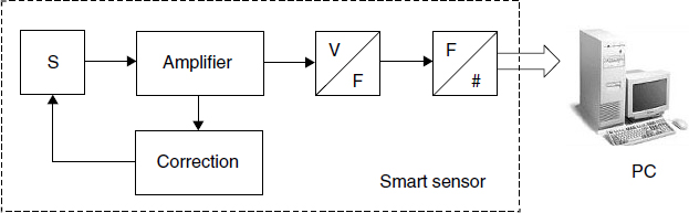
Figure 3.5 Smart sensor architecture with preliminary correction in analog domain and further conversion into frequency–time-domain signal
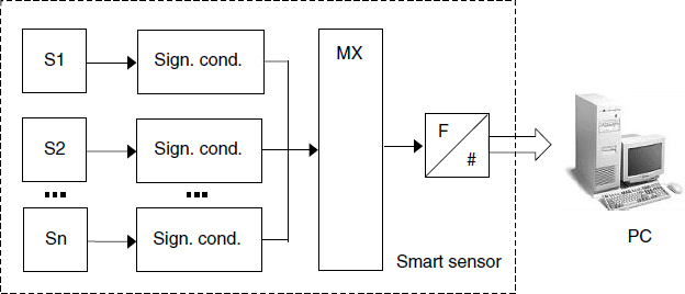
Figure 3.6 Architecture of a smart sensor array
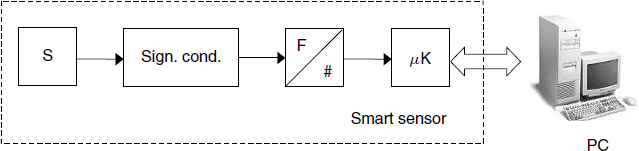
Figure 3.7 Smart sensor architecture with microcontroller
In the third example, a sensor element is connected via a frequency-to-code converter to a microcontroller (Figure 3.7).
The microcontroller can store the sensor's characteristic data in its internal ROM and, based on this information and the sensor signal, the microcontroller transfers the corrected signal to the bus. A very useful feature of such smart sensor architecture is that the microcontroller also permits the central computer to send data back to the sensor, which can be used to change the measuring range, to exert a recalibration or to adjust the offset.
As mentioned earlier, the microcontroller can itself realize the frequency-to-code conversion. In this case, the smart sensor architecture becomes simpler. Such an architecture is used to achieve smart sensor self-adaptation when depending on measuring conditions or measurands, the parameters of the method for frequency-to-code conversion will vary, for example, conversion time or accuracy of measurements.
In such a subsystem with the bus architecture, each sensor or a group of sensors can also contain a circuit, which can recognize addresses, this means the circuit can detect when communication between the sensor and the central computer is desired.
For many years, most of the described components of a bus system were separated and had their own housing. However, more recent developments have enabled the components indicated by the dashed lines in Figures 3.5–3.7 to be integrated into a single chip by the implementation of standard microelectronics library cells.
These typical smart sensor architectures are used for the creation of digital output smart sensors. Data transmission in the digital form excludes the inphase interference and the voltaic coupling of the sensor's output with the computer can be provided if necessary. Instead of buses, the binary encoded information can be transmitted into a parallel or a serial port. When parallel data transmission is feasible, the pulses representing the information arrive simultaneously at the central computer input making fast data transfer possible. However, in most cases the distance between the sensor and the computer is too far to permit parallel data transfer and so serial data transmission is required. The main advantage of such an approach is that it is not necessary to use any additional computer boards and specialized software drivers. All connections are external and drivers are standard. External connection provides an additional coupling in comparison with the usual data acquisition system with the bus connection. As the cost of microcontrollers continues to decrease, using a microcontroller at each measurement location will become affordable. In the future, many different signal-processing circuits can be integrated into the sensor chip. This approach is the next step to much wider distribution of intelligence. From Figures 3.5–3.7 the most important elements of a bus-oriented data acquisition system can be deduced. It is expected that starting with large data acquisition systems, analogue data transfer will gradually be replaced by digital systems.
DAQ boards for frequency–time-domain sensors are produced by many companies. They carry out data acquisition and data processing. Technical performances of some of them are shown in Table 3.1.
The maximum frequency and the number of channels meet modern requirements. But the accuracy is not perfect in order to use some of these DAQ boards with the modern frequency (period, duty-cycle, time interval) output sensors. Besides, it is desirable to have an opportunity to change both accuracy and time of the measurement directly during data acquisition.
3.4 Main Errors of Multichannel Data Acquisition Systems
The first measuring conversion in a channel of the data acquisition system is realised by a frequency (period) output sensor with information ability
Table 3.1 Technical performances of DAQ boards for frequency–time parameters of signals

and full-scale error γS. The set of sensors forms a data array, which is necessary, for example, for a control system. In view of the influence on the sensor of a significant number of destabilizing factors, which deform its transformation characteristic and result in occurrence of casual errors, the sensor's transformation error is distributed according to the unbiased normal law at which
where δmax and σsensor is the limit of sensor error and mean-root square error accordingly.
The second measuring conversion is analog–digital and accompanied by static and dynamic errors. In case of time interval measurements according to the classical indirect counting method (pulse duration, one or several periods of the sensor frequency), the static error is caused by the instability of the reference frequency f0, the inaccuracy of the time interval separation (the trigger error) and its quantization. In turn, the dynamic error is caused by the measurand changing during the time of measurement as well as one or several periods Tx and measuring cycles, especially in data acquisition systems using time-division channelling and a large number of sensors.
The limit error δmax and the mean-root square error σT values of the static error for the period (time interval)-to-code converter is determined by the following way:
where δTrigger_error and σTrigger_error, δ0 max and σ0, δq max and σq are relative, the limit and the mean-root square for trigger error, the reference frequency f0 and the quantization error accordingly.
Components of the common error of the direct counting method for frequency measurements in many respects are similar to those considered above except for the absence of the trigger error, so
In multichannel data acquisition systems multiplexers and communication lines between frequency output sensors and the computer as a rule do not influence the sensor's output frequency.
For reduction of the total error, it is necessary to reduce the weight of its components and, first of all, those with dominant values. In the case of frequency–time measurements, it is a quantization error. Its value is directly dependent on the method of the frequency (period)-to-code conversion. This is why the correct choice of a conversion method at the creation of data acquisition systems for frequency–time-domain sensors is one of the main tasks.
The central computer, processing the received data, carries out various mathematical calculations and forms the results array necessary for solution of different control and measuring tasks. This is the so-called third measuring conversion. In view of the above, the mean-root square error of the measuring channel in a data acquisition system σDAQ can be determined according to the following equation:
where σF/C = σf or σF/C = σT dependent on the method of the frequency-to-code conversion; σcalc is the mean-root square calculating error, carried out by a central computer. In the case of digital output smart sensors with architectures similar to those shown in Figures 3.5–3.7 the sensor error will already include the frequency (period)-to-code conversion error.
3.5 Data Transmission and Error Protection
Data transmission in the digital form from a digital output smart sensor to a remote central computer demands additional measures for error protection of transmitted data. It can be achieved by means of protective coding using various redundant codes. Very frequently cyclic codes are used. According to this, the common coding algorithm can be presented as: fxi(Txi) → Nparallel → Nserial → Ncyclic code. The cyclic (n, ninfo) code is the protective code each code combination of which is expressed as a polynom, having a degree not exceeding (n − 1) and divided on the generating multinomial (polynom) P(x) of nc = n − ni degree, where nc is the number of check bits, ni is the number of information bits and n is the code block length. The checking by the cyclic redundant code represents a method similar to the method of the control sum calculation, differing in that the cyclic redundant code has, as a rule, a two-byte length and is calculated based on the polynom of the divider. The cyclic code combination represents a 16-bit remainder of the division. Using such a method, at each moment of time, a block of a certain size is transmitted. Any transferred bit influences the cyclic code, therefore such an error check is most effective among similar methods.
The novel method of noise-resistant signal transmission in which the number of detected or corrected errors are increased twice is described below [91].
The complex solution of this task becomes considerably complicated for increasing transmission rate and length of code combinations. It especially appears by the creation of precision multichannel data acquisition systems, remote control and metering systems and digital wireless sensors and transducers. Such systems require increased correcting ability of the code without increase of the redundancy [92]. It requires the development of non-traditional methods, coders and decoders in view of factors influential to the choice of the correcting code, signal modulation, transmission rate and simplicity of realization.
3.5.1 Essence of quasi-ternary coding
The data coding depends on the right choice of method, which should ensure smaller redundancy of the correcting code at equal noise stability. Unlike conventional coding, quasi-ternary coding doubles the number of detected or corrected errors without a change in the number of check bits nc of the binary correcting code. The increase in the correcting ability of the quasi-ternary code is achieved by using signal redundancy, in addition to code redundancy. The code conversion is carried out with the help of the phase manipulator forming two various informative tags at ‘1’ and ‘0’ transmission of the multidigit codeword by digit-by-digit phase manipulation. This favourably differs from the absolute phase and relative phase modulation, offered by Professor N. T. Petrovich. According to the algorithm of digit-by-digit phase manipulation, the difference of phases of the carrier wave of the code signal (meander or harmonic) between any adjacent code elements is always 1800. Thus all bits of the code are transmitted: ‘1’ by the phase manipulations of one polarity, for example +1800, and ‘0’ by the opposite polarity [88]. It is possible also to use other types of manipulation, for example, the polar meander carrier wave or frequency, however, they concede to digit-by-digit phase manipulation.
The quasi-ternary serial code with the information ni and check bits nc of the correcting code that is transmitted by the digit-by-digit phase-manipulation signal is formed as a result of the code conversion. The code is self-clocked. It has the minimum value of the constant component and twin elements with the single or binary phase manipulation carrier wave for the denotation of the start and end of the codeword. The duration of its bits elements is a variable in bounds from 2.5 up to 3 periods T of carrier wave depending on the value of adjacent bits of the code [91–93].
Concerning correcting codes, it is expedient to use linear block cyclic separable codes. Unlike the other systematic codes, they correct not only single (independent), but also the group errors. Such codes are simpler in implementation, easily allow the introduction of redundancy at coding, if the level is insufficient, and select an informative part of the block at their decoding. This class of codes contains such codes as Bose–Chaudhuri–Hocquenghem (BCH) code and Golay code [94]. The algebraic theory for construction of block codes as well as coding and decoding algorithms were developed for them. The coding efficiency is determined by their redundancy, which can be varied in a wide range. The quasi-ternary coding can also be used for Hamming codes, group codes, iterated codes, codes with repetition and inversion, etc.
3.5.2 Coding algorithm and examples
Traditionally, the following operations are executed for coding by the separable cyclic code with a generating polynomial P(x) of xnc degree of the information group from the ni bits of the polynomial G(x): the symbol multiplying G(x) on xnc; the division of the obtained product on the polynomial P(x); the summation of the obtained residual R(x) with the product xnc. The obtained polynomial
contains the n bits. It has a necessary redundancy determined by its check bits nc = n − ni, and represents the polynomial of the separable systematic cyclic code, traditionally formed at transmission of the polynomial G(x) with the help of linear code filters with the shift registers and feedbacks. Thus, the following identity is valid:
indicating on the long division without the residual of the polynomial F(x) on the generating polynomial P(x). The identical is also used for decoding. All these operations are absent in the offered algorithm. In this case, the code filters are not used because the coder is performed by the ROM, which is a generator of check bits of the residuals R(x) of the unit matrixes Ini. The remainder R(x) required for the polynomial G(x) is formed only as a result of the summation to modulo 2. By the hardware realization the clock pulses counter controls the coder. The capacity of the counter is determined by the number of information bits ni. The values of check bits of the residual R(x) are determined by the nc adders. The ROM is used for the storage and bit-by-bit address reading of the residuals of appropriate rows in the unit matrix Ini of the polynomial G(x). Depending upon the information bit (‘0’ or ‘1’) in the decoder's input, the reading of the residual of a row in the unit matrix Ini of the given bit is forbidden or permitted. The summarization of the residuals at transmission proceeds until all information bits have arrived. Then the residual R(x), appropriate to one from 2ni values of the transmitted binary code is generated. Examples of coding that is carried out with the help of the above algorithm are shown below.
Example 1. Coding of the polynomial G(x) by the Golay code with parameters (23, 12) and the generating polynomial P(x) = x11 + x9 + x7 + x5 + x + 1 = 101011100011, at n = 23 bits; ni = 12 bits; nc = 11 bits; d = 7 is the code distance; s = 3 is the number of correctable errors; r = 6 is the detectable error).
The generating matrix C(23, 12) is the following:

The coding of the polynomial G(x) = 111000011001 at transmission by the quasiternary code is shown below.
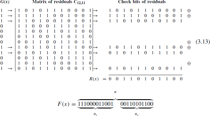
It is easily proved that the identity (3.11) will be realized by division of the generated polynomial F(x) by the generating polynomial P(x).
The time diagram for the generated digit-by-digit phase-manipulated signal of the noise-resistant quasi-ternary code at the start-stop transmission mode using a meander or harmonic carrier wave is shown in Figure 3.8. The Golay code with parameters (23, 12), applied in the example is one of a few nontrivial perfect binary codes [94].
There is also the so-called extended Golay code with parameters (24, 12) and with higher efficiency (d = 8; s = 3; r = 7). The coding is realized similarly to Equation (3.13). It is necessary to provide an additional check bit, determined by the polynomial P(x) = x9 + x8 + x5 + x4 + x2 + x.
Example 2. Coding of the polynomial G(x) = 1110 001 by BCH code with parameters (15,7), that is given by the generating polynomial P(x) = x8 + x7 + x6 + x4 + 1.
After construction of the generating matrix Cn,ni for the BCH code (15,7) C15,7 = |I7T ||C7,8| using the residual matrix C7,8, let us form the code combination F(x) of the BCH code for the polynomial G(x) = 1110001 transmission companion to Equation (3.13):
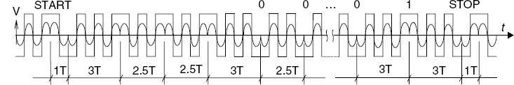
Figure 3.8 Digit-by-digit phase-manipulated quasi-ternary coding

It is easy to prove that the identity (3.11) is true. The generated code F(x) has the code distance d = 5 (s = 2 or r = 4). The quasi-ternary code, obtained from the BCH code (15,7) after decoding will ensure s = 4 in the error-checking mode and r = 8 in the error-detection mode. The time diagram of the generated quasi-ternary code for the first five bits of the polynomial G(x) coincides with that mentioned above. The signal redundancy increases the coding efficiency without increasing BCH code redundancy.
3.5.3 Quasi-ternary code decoding
The reception of the self-clocking digit-by-digit phase-manipulated signal of n-bit quasi-ternary correcting code is carried out by two non-linear phase selectors. The selectors are quasi-optimal integrated receivers, which differ by a small time response. The probability of the error is determined as
In the case of the harmonic carrier wave we have
where: Veff_signal and Veff_noise are the effective voltage of the signal and noise accordingly; ΔF is the transmission bandwidth of the input filter; B is the signal manipulation speed.
Two code combinations are formed from the receipted code combination of the quasi-ternary cyclic code in the inputs of phase selectors. The first combination F′1(x) contains only impulses of positive phase manipulation ‘1’, and the second F′o(x), only impulses of the negative phase manipulation ‘0’. Each of them can be true, i.e. to coincide with the transmitted code combination as well as false because of the noise effect. The decoding according to the algorithm, assigned by the decoder, will be realized simultaneously with the bit-by-bit input and storage of the n-bits polynomials F′l(x) and F′0(x).
In the case of decoding with error correction the division will be realized with the aim of determining the identity (3.11). If some errors are present in one or both code combinations, the following identities with allowance (3.11) will be used:
where δ1i(x) and δ0i(x) are the syndromes of error vectors E1i(x) and E0i(x), arising in the polynomials F′1(x) and F′o(x), that do not depend on the transferred polynomial F(x) and are determined only by the position of error in the code combination. All methods for error-position detection with the consequent correction are based on the analysis of syndromes S1i(x) and S0i(x). Its realization becomes considerably according to increasing number of corrected errors. Therefore the number S is restricted by the inequality S≤3.
Decoding by the error detection mode is simpler, as it is based on the sum to modulo 2 and comparison. As more expedient, only this mode is further considered, especially in the case of codes with high degree polynomials P(x) and large code distance dmin. It is stipulated by the following factors:
- The detecting ability of the cyclic code at the same redundancy is higher than the correcting ability (r = 2s).
- The number of logical and other operations that should be executed by the decoder is significantly less in comparison with the number of operations for their correction.
- The reliability of decoding is higher, as for the given code efficiency it is possible to reduce the code distance dmin and with allowance the quasi-ternary coding, the check bits decrease twice.
For this reason decoding in the detection mode is widely used in different systems:
- With the make-decision feedback, where the BCH code with generating polynomial P(x) = x16 + x12 + x5 + 1 is used.
- Without the feedback, but using the reception with erasure and the possibility of restoring the erased code units, due to its redundancy.
The analysis of the noise stability has shown that decoding in the error-detection mode is more preferable for independent errors with the probability p = 10−5 − 10−3 as the noise stability increases up to 2 − 3 orders for the cyclic with d = 3 and up to 3 − 4 orders for the code with d = 4.
The decoding algorithm contains operations, which are executed up to the termination of arrival of the phase-manipulated signal of the quasi-ternary cyclic code in the following sequence:
- Creation from the received n-bits code combination of the polynomial F′(x) the polynomials F′1(x) and F′0(x) containing only ‘1’ or ‘0’ accordingly, recording in the buffer register the F′1(x) and F′0(x) after inverting bits.
- Selection from F′1(x) and F′0(x) the informative ni bits polynomials G′1(x) and G′0(x) and creating according to the algorithm (3.13) the check bits of appropriate strings of the unit matrix Ini of the residuals R′1(x) and R′0(x), stored in the ROM.
- Selection of the received polynomials of residuals and their comparison with the residuals R′1(x) and R′0(x) by execution of the following operations:
- the equivalence and signal forming for the reading of the polynomial G(x) from the buffer register at the moment of arrival of the ‘STOP’ signal (Figure 3.8)
- the non-equivalence and signal forming for prohibiting the reading of the polynomial G(x) because of errors in the received code combination.
The full coincidence of compared polynomials of residuals is informed by the signal of the absence of error (ER = 0).
This novel method of the efficiency rise for coding without increasing the code redundancy of the used code by use of signal redundancy has confirmed the high efficiency in practice. The additional increase of the code redundancy considerably increases the detecting ability of the cyclic code. Searches for the algorithm simplification for the error correction in code combinations of the quasi-ternary code (Patents No.107 54 37, 1146 788, 1124 363 (USSR), [88]) are continuing.
The use of PGA or FPGAs allows multifunctional programmed devices containing the check bits of matrixes Ini,nc. Thus, the choice of the required code redundancy for many perspective codes can be realized. The offered non-traditional method of coding promotes the further rise of the coding efficiency by using generating polynomials P(x) of high degrees–14, 16, 24 and 32.
Summary
The method of data acquisition with time-division channelling allows inexpensive multichannel data acquisition systems for quasi-digital sensors.
The method of data acquisition for quasi-digital sensors with space-division channelling is becoming increasingly attractive due to the low cost of frequency-to-code converters. A separate frequency-to-code converter for each channel realizes a much higher polling frequency for each channel.
The accuracy of modern industrial DAQ boards for frequency–time parameters of electric signals often does not allow using them together with modern precision frequency (period, duty-cycle, time interval) output sensors. Also, it is desirable to have an opportunity to change both the accuracy and the measurement time directly during data acquisition.
The quantization error has the essential influence on the data acquisition system's accuracy. Its value is directly dependent on the method of the frequency (period)-to-code conversion. That is why the correct choice of a conversion method by creation of data acquisition systems for frequency–time-domain sensors is one of the main tasks of the system design.
Data transmission in the digital form from a digital output smart sensor to a remote central computer demands additional measures for the error protection of transmitted data. It can be achieved by means of protective coding using of various redundant codes. Very frequently cyclic codes are used for this aim.
Taking into account individual features of the chosen correction methods, transmission devices and specificity of system application, developers of data acquisition system should solve which requirements the coding algorithm would best meet.