
2
CONVERTERS FOR DIFFERENT VARIABLES TO FREQUENCY-TIME PARAMETERS OF THE ELECTRIC SIGNAL
Apart from the various types of frequency sensors considered below there is another big group of analog sensors with current, voltage or resistance output. These are, for example, thermocouples, potentiometric sensors etc. When using the frequency signal as the sensor's informative parameter, it is expedient to use voltage (current)-to-frequency converters of the harmonious or pulse signal in the measuring channel. Such converters are frequently used in practice due to their good performance: linearities and the stability of transformation characteristics, accuracy, frequency ranges, manufacturability and simplicity.
2.1 Voltage-to-Frequency Converters (VFCs)
The operational principle of majority VFC consists in alternate integration of input voltage and generation of pulses when the integrator's output voltage equals to the reference voltage. VFC with continuous integration have special advantages. Such converters do not require additional time for returning the integrator to an initial condition at the beginning of a new conversion cycle.
Initially such converters were developed based on magnetic materials with a rectangular hysteresis loop. These were the elementary magneto-transistor multivibrators with input frequency directly proportional to the input voltage [65,66]. Various modifications with improved characteristics and possibilities [67–69] were further developed. For example, a pulse-width modulator with constant amplitude of output pulses and direct proportionality of the duty factor to input voltage has been described in [67]. A magneto-transistor multivibrator with high sensitivity (1000 Hz/mV), 1000 Ω input resistance for usage in VFCs for sensors such as thermocouples, resistive thermometers and strain gauges [68] has been developed. It has a voltage range 0–20 mV at nonlinearity of transformation characteristic ±0.4%. The high initial frequency of the input signal 250 kHz essentially reduces the transient time and the drive circuit's inductance. The distinctive feature of the multivibrator offered in [69] is its use for the linear transformation of positive as well as negative voltage into frequency. However, the use of VFCs with magnetic elements has not received a wide distribution for the precise transformation of the voltage (current) into a pulse-frequency signal because of the strong dependence of the core's parameters on temperature. The suggested circuits for the temperature compensation were too complex and did not allow the complete exclusion of temperature influences.
The development of integrating VFCs based on symmetric controlled multivibrators was made in parallel. They differed by simplicity and high technical and dynamic characteristics [70,71]. Working in multichannel code-pulse remote metering systems with frequency output sensors in the industrial environment in temperatures up to +50 °C, VFCs reliably carried out linear transformation of the voltage 4–45 V into frequency signals 1.8–20.0 kHz. They guaranteed nonlinearity of the transformation characteristic not worse than ±0.2% and relative temperature error up to ±0.5 % [72,73]. In the patent [71] it is described how the authors removed the nonlinearity error caused by the non-identity of the two driving current circuits, providing the linear charge (or discharge) of integrating capacitors in the multivibrator. It was achieved due to the usage in the multivibrator of one driving current transistor instead of two.
It has been demonstrated, that by using stricter requirements to the conversion accuracy, it is expedient to use similar integrating elements, for example, the charge of the capacitor and the compensation of it by the discharge impulse with constant amplitude. Therefore, the most acceptable for usage in integrated VFCs were:
— Integration with the help of the capacitor (change of the multivibrator's frequency by the change voltage, the current or the resistance). The range is 10–100% and the basic error is 0.5%.
— Charge of the capacitor by the direct current proportional to the measurand and the fast discharge by achievement of the threshold level (the range is 0–100%, the fiducial error is 0.3%).
— Charge and discharge of the capacitor by the direct current proportional to the measurand (the range is 0–100%; the fiducial error is 0.1%).
Creation of operational amplifiers and other elements of microelectronics have opened a way to design more perfect integrators and the VFC on the basis of new principles of integration.
VFCs of direct transformation with open structures, and VFCs of the compensatory type with feedback [74–76] can be defined. Among the open-type VFCs greatest distribution has been received integrating converters based on the cyclic charge during time T0, and the discharge during Tdischarging of the integrator's integrating capacity (Figure 2.1a).
The main source of methodical error is the time off T0 during which the integrator is prepared for a new cycle of transformation Vx → fx (i.e. comes back to an initial state). Reduction of this error requires the inequality satisfiability T0 ![]() Tdischarging, and its suppression T0 = 0. A more radical method of error suppression is to use two alternatively working integrators (Figure 2.1b), or the usage of the integration and the ‘disintegration’ (Figure 2.1c). In these cases, the methodical error will be completely suppressed.
Tdischarging, and its suppression T0 = 0. A more radical method of error suppression is to use two alternatively working integrators (Figure 2.1b), or the usage of the integration and the ‘disintegration’ (Figure 2.1c). In these cases, the methodical error will be completely suppressed.
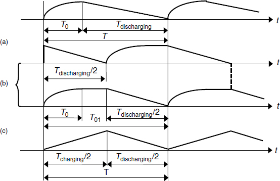
Figure 2.1 Charge and discharge diagrams of integrating capacitors

A simple VFC containing two integrators based on operational amplifiers is shown in Figure 2.2.
Each of the integrators is working alternatively, continuously–cyclically without dividing pauses between cycles, due to the RS-trigger with comparators on inputs. The trigger is nulled each time an input voltage of one of the integrators equals the stable reference voltage V0. Owing to the comparator's output the signal will toggle the RS-trigger in the opposite state. One of the switch discharges the integrator's capacitor and the second starts a new cycle of integration of the input voltage Vx –the described process is then repeated.
VFCs with feedback [74–76] have higher accuracy, stability and the opportunity for sensor signal processing with a low level of input signal, compared with open-type VFCs. The most preferable is a VFC with pulse feedback. Some basic types [76] will be considered below.
The VFC including an integrator based on an operational amplifier, a comparator and impulse feedback loop is shown in Figure 2.3. With the help of feedback loop the pulses with stable volt-second square S0, amplitude V and duration τ0 are periodically formed.
At integration of the input voltage Vx, the voltage V of the integrator's output reaches the comparator's threshold. This drives the impulse feedback loop, which forms a pulse V0 whose polarity is opposite to the polarity of the input voltage. With the feedback impulse S0 on the integrator's input the voltage is linearly increasing during time t0. Further, under the influence of the voltage Vx the integrator's output voltage is decreasing to reach the comparator's threshold. Then the conversion cycle of Vx → fx is repeated again. The VFC's output frequency while forming the impulse feedback is.
For an ideal integrator, the output frequency is proportional to Vx and does not dependent on the feedback pulse form. Only the stability of the volt-second square S0 is important, which is not a difficult technical task.
Another version of a VFC with impulse feedback, but with separate formation of amplitude V0 and the duration τ0 is shown in Figure 2.4. It contains an integrator and a comparator based on operational amplifiers A1 and A2; a D-trigger is applied, a clock then inputs reference pulses of frequency f0 min = 2.5fxmax, the voltage reference, the analog switch and resistors R and R0 of integrating circuits of the input and reference voltage source.
This VFC functions almost like the previous VFC (Figure 2.3) except that at the comparator operation, the input signal operates on the D-trigger's input, and at receipt of the first impulse of the reference frequency f0 on the trigger's clock input the last one is toggled and produces the driving pulse for the analog switch. Thus by the integrator's input through the resistor R0 the reference voltage V0 is connected. After the capacitor has been discharged, the comparator E0 is returned to an initial stage by the pulse of frequency f0. The D-trigger is also returned to the initial stage and disconnected from the integrator reference voltage V0.
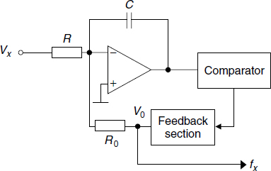
Figure 2.3 VFC with impulse feedback loop
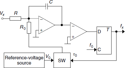
Figure 2.4 VFC with impulse feedback and separate forming of amplitude V0 and duration τ0
There are the following sources of the VFC conversion error:
- inaccuracy and instability of the R0/R ratio
- inaccuracy of integration
- instability of the comparator's threshold during one conversion cycle
- absence of synchronization of pulses f0 with the moments of the comparator operation
- instability of the reference voltage V0
- instability of the time interval τ0.
The use of the appropriate circuitry and technological measures may reduce the errors of Vx → fx conversion listed above.
Further modification of the circuits considered above, which allows reduction of the nonlinearity error and the error due to synchronization absence between the moments of the comparator operation and the beginning of the feedback impulse forming is shown in Figure 2.5. It is achieved by the additional J–K trigger, the coincidence circuit, the frequency divider with division factor n and increasing the reference frequency f0 by n times.
Due to the increase in frequency f0 by n times and the use of the frequency divider with the division factor n on the J–K trigger's input the feedback impulse duration remains constant and equal to:
However, the maximal delay of the D-trigger operation is decreased and does not exceed 1/nf0. Due to this, the VFC accuracy is increased.
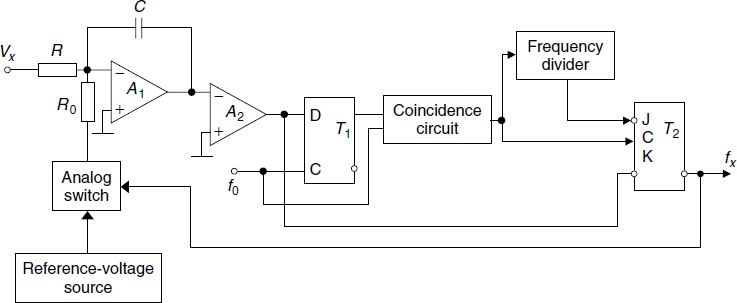
Figure 2.5 VFC modification with impulse feedback
Let us consider principles of operation, features and technical performances of some interesting integrating VFCs with a pulse feedback.
The full-range VFC is based on the balanced charge and discharge of the integrator's capacitor. It was created for the functionality extension of the digital frequency counter for positive voltage, current and capacitance measurements [77,78]. Its circuit is shown in Figure 2.6 and comprises an integrator, a comparator, a digital univibrator based on a pulse counter and a quartz generator, a signal conditioner, a source of stable current i and a high-speed transistor differential current switch.
The conversion is performed continuously–cyclically without dividing pauses. During the first part of the cycle the input current Ix is integrated and during the second, the difference of currents Ix and i. Its duration is equal to the pulse width Tx of the output frequency fx. The distinctive feature of the method [78] is the equality of quantity of electricity on the integrator's input and that consumed by the source of current through the high-speed differential switch, which is carried out for some VFC cycles because of uncertainty of the time delay of the digital univibrator operation within the limits of 0.125 μs. The measuring conversion's equation may be deduced as follows.
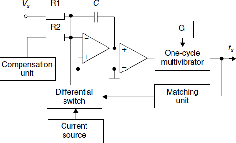
Figure 2.6 Full-range VFC based on balanced charge and discharge of integrator's capacitor
The charge Q1 acting during the time Tx to the integrator's input from the source of voltage Vx is equal to:
and charge Q2 consumed from the integrator's input by q = iτ equals:
where N is the number of positive pulses on the univibrator's output; τ is the pulse duration.
From the condition of equality Q1 = Q2, reflecting the principle of the VFC operation, it follows that
where k is the conversion factor of the VFC. Hence the conversion Vx → fx is linear, and δfx = δk.
Taking into account the following values from the circuit R = 107 Ω, i = 2 × 10⁻⁴ A, τ = 5 × 10⁻⁷ s the following equation for the direct readout is obtained:
The formula for current conversion is obtained in a similar way:
As follows from Equation (2.5) the main VFC error (instability) is determined by the elements of its pulse compensating feedback. The instability of the integrator's capacitance, threshold of the comparator operation and the time delay of the digital univibrator practically do not influence the VFC operation.
The VFC can work in a wide range of positive measuring voltages 1 mV–1000 V without any switching as well as currents in limits from 10−10 up to 10−4 A and higher with the help of additional shunts. Together with a digital frequency counter and time of measurement Tx = 1 s it is possible to measure the voltage of positive polarity with the frequency error not exceeding 10−3fx ± 0.1 Hz. This VFC can be used similarly to the controlled by voltage full range 10–106 Hz linear generator.
A voltage-to-frequency converter is shown in Figure 2.7. It realizes the voltage-to-frequency conversion according to the method of binary integration [79]. At relative simplicity and minimum hardware, this VFC achieves high accuracy for a wide range of input voltages Vx.
This VFC contains an integrator based on an operational amplifier, a control switch, a quartz generator, a threshold device and a time interval shaper of constant duration 0.1 s.
The Vx → fx conversion is carried out in two steps. At the first step (duration T1), only the voltage Vx of negative polarity is integrated, and at the second step (duration T0) both the voltage Vx and the reference voltage V0 are integrated simultaneously. During step T1 the input signal acts through the resistor R1 on the inverting integrator's input, the control switch will be closed. Thereafter the output voltage of the integrator is increased, and the greater Vx, the greater its steepness and less the duration T1. As soon as it reaches the threshold value the threshold device acts and drives the impulses of the quartz generator on the time interval shaper's input. By the pulse propagation through the shaper's divider the first voltage transition from ‘1’ to ‘0’ logical level on the shaper's output opens the control switch. The time interval T0 which is forming begins with the same moment, during which voltage V0 is acting on the inverting integrator's input through the resistor R0. Its polarity is opposite but the amplitude is much higher. As a result, the output voltage of the integrator will be linearly decreasing. After the second transition from ‘0’ to ‘1’ the forming of the time interval T0 is finished, the switch is closed, the pulse propagation of the quartz generator into the pulse shaper is stopped and the VFC is again in the mode of integration, only the input voltage Vx. Thus the averaging periodic process of conversion is realized in the VFC.
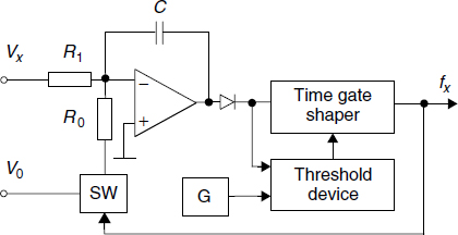
Figure 2.7 VFC based on method of binary integration
Idealizing the operation of the VFC's units, the steady state can be described by the following equation:

where k1 and k2 are the integrator scaling for the measuring and compensating signals accordingly; T is the working cycle of the VFC during both conversion steps. Consequently T = T1 + T0.
If the voltage Vx is constant during the readout period, Equation (2.8) can be written:
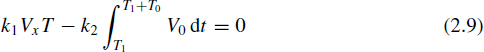
Otherwise the integral in Equation (2.8) may be replaced with the product VxT, where Vx is the average input voltage during the time (T1 + T0) = T. After simple transformation, we obtain the linear dependence of the measuring transformation:
is the volt-second square of the feedback impulse,
The analysis shows that the function of the measuring conversion of the VFC is determined by the size of the volt-second square of feedback impulses and the ratio of the summing resistance on the integrator's input. It is obvious that the VFC accuracy at first approximation depends on the stability of the specified parameters. Thus the advantage of closed compensation VFC circuits above open circuits.
The above-considered VFC has a high enough conversion factor (10 kHz/V) for the measuring interval 0.1 s and can be increased. The resolution is 1 mV, and the conversion error is 0.05%.
Another voltage-to-frequency converter [80] in comparison with that considered above converts the voltage Vx to the output frequency fx as a result of continuous tracing compensation by two input Vx and compensating Vcompensated voltages which act in the feedback loop as a result of the return transformation of the output frequency fx. This converter differs from other such VFCs in that the impulse shaper of the stable volt-second square is entered into the feedback loop. Due to this, the reliability and accuracy of conversion are essentially increased.
The circuit of such a VFC is shown in Figure 2.8 and consists of the subtracting unit carrying out the function of the comparison element of Vx and Vcompensated voltages and forming the voltage difference ΔV = Vx − Vcompensated and two circuits–direct and indirect. The direct circuit consists of an amplifier of the direct current and a controlled generator. Usually in the direct circuit, high-sensitivity and less stable converters are used. The feedback loop, in which as a rule, highly stable converters of homogeneous size are used, consists of the impulse shaper of the stable volt–the second square, the voltage divider, the integrator, the pulse-amplitude modulator and the fixing element.
The Vx → fx conversion is realised by the following way. The input voltage of undercompensation ΔVx on the subtracting unit's output is transformed in the direct circuit into the output frequency fx. In the steady state the frequency fx of the controlled generator is proportional to the voltage Vcompensated. The integrator realizes the integral from the sum of two voltages: V1 from the pulse shaper's output and V2 from the fixing element's output. The output voltage of the integrator is acting once per period Tx through the pulse-amplitude modulator to the fixing element. Both of these elements form the negative feedback loop. As a result, the voltage V2 on the fixing element's output is equal to the average voltage during the period T, acting from the pulse shaper's output of the stable volt–the second square and is equal to:
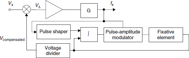
Figure 2.8 VFC of tracing compensation type
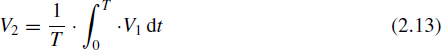
Thus, on the pulse shaper's output there are pulses stabilized on the amplitude V0 and the duration τ0. As a result, the voltage Vcompensated on the voltage divider's output within the size of undercompensation ΔV can be accepted to be equal to the converted voltage Vx. In view of the transfer factor k of the voltage divider, we will receive the required linear dependence between the frequency fx and the input voltage Vx:
This VFC of the tracing compensation type provides increased reliability and accuracy of measuring instruments and ADC, working in data acquisition systems.
Let us deduce the basic equations describing a static VFC at which the balance of the measuring circuit is incomplete. We shall notice that due to the presence of the undercompensation voltage ΔV = Vx − Vfeedback = fx/kdc the balance of the circuit is provided, though ΔV is a source of the static error, the value of which can be reduced up to a minimum [81,104].
Let us consider the common block diagram of a static VFC (Figure 2.9). We shall accept that the subtracting unit is the converter of the circuit of the direct conversion of ΔV and we shall deduce some basic equations describing its operation and characteristics [81].
For the state stage taking into account the linearity of characteristics of measuring transformations and conversion factors of the subtracting device ksub, factors of direct kdc and indirect kid conversions, the following equations are valid:
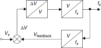
Figure 2.9 Common block diagram of a static VFC
Having carried out transformations and solved the equation relative to fx we have:
Hence, the conversion factor of the VFC or sensitivity of balancing is
with value determined by units of measurements fx, Vx and it is in (1 + ksubkdckic) times less than kdc but for this reason as will be shown below, the conversion accuracy, the voltage range and the signal-to-noise ratio will be increased at the same time.
For the case when ksubkdckic ![]() 1
1
It specifies that metrological and dynamic characteristics of the compensation VFC are completely determined by similar characteristics of the indirect conversion. After taking the logarithm, the differentiation and the transition to the final increments we have:
For the case when the condition ksubkdckic ![]() 1 is not valid, we have:
1 is not valid, we have:
and after taking the logarithm, differentiation and transition to the final increments
For the most typical case, when ksub = 1, we have:
Hence, the multiplicative component of the error in the circuit of the direct conversion has been decreased (1 + kdckic) times. Moreover, if errors δkdc and δkic are caused by the same reasons they are subtracted.
Other characteristics of the VFC are the following:
- The balancing depth (kdckic) or the loopback amplification is equal:
- The statism kstat or the relative balancing error, equal to the ΔV is always constant from the input value
- The relative balancing depth:
Taking into account received characteristics
Neglecting the error δksub owing to its smallness we have:
In order that the conversion error including the δkstat is insignificant, it is necessary that kstat ![]() 1. The limit of kstat reduction is the loss of the system stability at which there is an abnormal mode of the Vx → fx conversion. The optimum values kstat and the loopback amplification are the following:
1. The limit of kstat reduction is the loss of the system stability at which there is an abnormal mode of the Vx → fx conversion. The optimum values kstat and the loopback amplification are the following:
It is necessary to note that apart from the high speed, the absence of the conversion error caused by the incomplete balancing is another important advantage of such a VFC. Since this error has a regular character it may be taken into account by the VFC graduation. It is possible because kstat does not depend on the measuring voltage Vx, therefore it may be easily corrected. The conversion error because of ΔV will take place only in the case of the statism inconstancy. However, it can be reduced by calibration of its regular, i.e. constant component.
The distinctive feature of the VFC with switching of the integration direction is the use of the capacitor recharging for conversion of alternating voltages. Such a VFC consists of the control charging devices, switches, an integrating capacitor, a comparison device of the reference voltage and the capacitor voltage and a control trigger (Figure 2.10).

Figure 2.10 VFC with switching of integration direction
The VFC works as follows. The voltage Vx is applied to the control charging device's input, the output current of which is the charging current of the integrating capacitor. If, at the first moment, the switches SW2, SW5 are closed and SW3, SW4 opened, the circuit I charges the integrating capacitor. Therefore
At the moment of equality Vx = V0, the pulse, which switches the control trigger, is formed. Switches SW2, SW5 are opened, and SW3, SW4 closed. The new circuit of the capacitor charge is formed under the current influence, the integrating capacitor is recharged and the potential in point 2 is changed from −V0 up to +V0. At the moment of equality V2 = V0 the process begins again. We shall notice, that in both cases, the potential in point 1 (in the first case) and point 2 (in the second case) grows linearly up to the reference potential with a speed proportional to the value of the input voltage Vx. Thus, there are oscillations in the circuit. We will have pulses, whose frequency depends on the value of the input voltage Vx on the comparison device's output.
The charger device supports the current Icharge constant at the integrating capacitor charging at constant Vx. The voltage on it depends linearly on time. From Equation (2.32) we find the time Tx of the capacitor recharging from −V0 up to +V0 and the basic equation for the Vx → fx conversion:

where k is the conversion factor of a charger device.
It is obvious, that in order to have the linear dependence of the VFC's output frequency on the value Vx it is necessary for the integrating capacitor to have stable parameters, constant reference voltage, and a charger device with a straight-line characteristic and large stabilization of the current Icharge. The experimental results are the following Vx = (0.1–1.5) V; fx = (500–20 000) Hz; the nonlinearity error is 0.3%.
The best VFCs have almost as good performance and provide unique characteristics when used as analog-to-digital converters, but are relatively slow. A lot of VFC converters exhibit some nonlinearities in comparison with dual-slope converters.
New architectures of integrated VFC converters with the charge-balance, the inversed VFC, the synchronized VFC and a relatively fast synchronous version of a VFC with the charge balance were recently described in [82]. Their versatility, excellent resolution, very wide dynamic range and an output signal that is easy to transmit often provide attributes unattainable with other converter types. Since the analog quantity is represented as a frequency of a serial data stream, it is easily handled in extensive industrial multichannel systems. Virtually unlimited voltage isolation (tens of thousands of volts, or even more) can be accomplished without loss in accuracy using low-cost optocouplers or fibre optic links. At the other end, the digital signal can be either digitally processed or reconstructed to analog, which is useful in many, for example, medical, applications. A VFC possesses true integrating input and features the best noise immunity, much better than a dual-slope converter. It is especially important in industrial measurement and data acquisition systems.

Figure 2.11 Voltage-to-frequency converter with charge balance and its time diagrams (Reproduced by permission of Silesian Technical University)
A voltage-to-frequency converter is actually a kind of precise relaxation oscillator. Nearly all modern VFCs use a well-proven charge-balance technique to control the output frequency, as shown in Figure 2.11.
The integrator produces a two-part linear ramp: the first part (T1) is a function of the input voltage, the second (T2) is dependent on both the input voltage and the constant reference current. The oscillation process forces a long-term balance of the charge (or time-averaged current) between the input current and the reference current:
If
then
If both resistors R1 and RR are identical, the result of conversion is independent of drifts of the integrating components. The converter's integrating input properties make it ideal for high noise industrial environments and guarantees excellent noise immunity by smoothing the noise effects. Every change in the input signal always affects the output in the current or the next conversion cycle so averaging consecutive results improves overall accuracy and noise attenuation.
The accuracy of a VFC depends mainly on the period T2 of the one time. In precision, synchronous VFCs in this critical period T2 are accurately derived from an external, crystal controlled oscillator (Figure 2.12). When the integrator negative-going ramp reaches zero, the integration of the input signal will continue, awaiting the clock pulse. Output pulses align with clock pulses, which cause the instantaneous converter output frequency to be a subharmonic of the clock frequency. The time intervals between pulses become not equal, but the average frequency is still an accurate analog of the input voltage. The output may be presented as a constant frequency, which is locked to a submultiple of the clock frequency, with occasional extra pulses or missing pulses.

Figure 2.12 Synchronized voltage-to-frequency converter and its time diagram (Reproduced by permission of Silesian Technical University)
All voltage-to-frequency converters exhibit some nonlinearities in comparison with dual-slope converters. The linearity performance decreases and the gain error increases with the full-scale operating frequency. It is obvious that the integrator in a dual-slope converter changes the direction of the output ramp about 10, 20 or 50 times per second, in a VFC a few thousand or even more. Delays in the integrator and analog switches generate errors coupled with every transition and are proportional to the output frequency.
When the system utilizes a VFC, an appropriate frequency measurement technique must be chosen to meet the conversion accuracy and speed requirements. The commonly used method for converting the output of a VFC to a numerical quantity is to accumulate the output pulses in a gated counter. The quantization error can be made arbitrarily small by counting with long gate times. However, many applications require relatively fast conversions (short gate periods) with high resolution.
The inversed VFC integrating analog-to-digital converter seems to be quite attractive. In this converter, the input signal is continuously integrated, as in the VFC and Elbert's converters, providing excellent noise immunity. Working very much like the dual-slope ADC, it features similar, or even a little better, properties. The circuit, presented in Figure 2.13 differs slightly from the dual-slope architecture–one of the switches is removed. Actually, it's very similar to the V/F converter configuration.
Figure 2.13 Integrating inversed VFC and its time diagrams (Reproduced by permission of Silesian Technical University)
As in other integrating converters, the integrator produces a two-part linear ramp: the first time period (T1) is constant, the second (T2) is dependent on the input voltage and the constant reference voltage of the opposite polarity. During the time T1 only the input signal Vx is integrated and the integrator's output ramps linearly to the level proportional to the input voltage. In the second phase of conversion the reference voltage VR is also switched to the integrator input, which processes to integrate in an opposite direction. The length of the time T2 the integrator output requires to get back to zero depends on the input voltage level and is equal to zero for the grounded input, but goes to infinity for IX close to IR. When the ramp reaches zero, the comparator activates the one-shot for the period T1. This disconnects the reference voltage from the integrator input again. Integrator slopes are both established by the same integrating capacitor and the two resistors' ratio, so these parameters need to be stable over one conversion time. The integrator's swings during both phases of conversion are equal and the capacitor charge is balanced:
These equations are exactly the same as Equation (2.36), describing the voltage-to-frequency converter; however, both converters behave quite differently–the time T2, not T1, is constant in a VFC. According to these similarities and differences the name of this converter is the inversed VFC, or the IVFC.
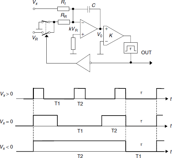
Figure 2.14 Modified inversed VFC and its time diagrams (Reproduced by permission of Silesian Technical University)
The primary circuit can be modified. Figure 2.14 shows one of the possibilities.
A voltage divider with the attenuation 1/k connected to the reference source offsets the non-inverting input of the operational amplifier. An analog switch connects the reference resistor RR to the ground during the phase T1 and to the voltage VR during T2, so the inverting input of the operational amplifier always sees the constant resistance. The following equation describes the charge balance during the conversion period T1 + T2:
For RI = RR and k = 0.25
In this case, the circuit converts the bipolar input voltages. If the input ranges is limited to ±0.25VR, T2 changes from 0.33T1 to 3T1; for Vx = 0, T2 = T1.
This converter shares many properties of other integrating dual-slope ADC, AFC and Elbert's converters. Its integrating input characteristics provide excellent noise immunity in industrial environments. The time-related, two-phase output signal is almost as easy to transmit as in Elbert's converter and also contains information about the input polarity. This signal can be easily isolated using opto-couplers or fibre-optic lines and can be interfaced to many commonly used microcontrollers and microprocessors through the counter input port or the timer/counter peripheral ICs. The accuracy is comparable with the dual-slope, while the noise immunity and the ease of transmission to VFC or Elbert's converters. For determining the result of the conversion, times T1 and T2, or only the duty factor DF should be measured. The transmitted digital signal can be not only digitally processed, but also reconstructed to the analog one.
A growing proportion of complex data acquisition and control systems today are being controlled by microprocessors or other programmable digital devices. As mentioned, the use of voltage-to-frequency converters requires an appropriate frequency measurement technique. Although it is not a very fast conversion method, a VFC system conversion speed can be optimized. In the most frequently used approach output pulses of the VFC are accumulated in the gated counter during the constant time. Since the gate period is not synchronized to the VFC output pulses, there is a potential inaccuracy of plus or minus one count–the resolution is related to the gate period and to the full-scale frequency of the VFC. The quantization error can be made small by counting with long gate periods and using high output frequencies, but the VFC linearity degrades at high operating frequencies and this limits the accuracy. On the other hand, long gate periods limit the conversion speed. Many applications require relatively fast conversions with good resolution and accuracy. The ratiometric counting technique partially eliminates this tradeoff; by counting n counts of a high speed clock (independent of the VFC clock) which occur during an exact integer N counts of the VFC, an accurate ratio of the unknown frequency Fx to the reference frequency so the n count is a large number. The one-count error causes a small effect on the conversion result. The two counts (n and N) are divided in a host computer or a microcontroller, giving the final result. Since the synchronized gate waits complete cycles of the VFC to achieve an exact count, a very low frequency would cause the gate period to be excessively long. This can be eliminated by offsetting the zero-input frequency to be constant and stable, and time intervals between pulses are exactly equal. Unfortunately, in precision, synchronous voltage-to-frequency converters (as in Figure 2.12), these conditions do not occur.
Figure 2.15 shows a modified, precision and relatively fast synchronous version of a VFC with the charge balance.

Figure 2.15 Modified ‘fast’ version of a VFC (Reproduced by permission of Silesian Technical University)
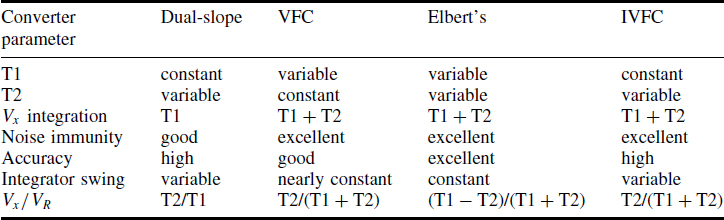
Table 2.1 Summarized typical parameters of different integrating converters (Reproduced by permission of Silesian Technical University)
In this converter the disintegrating period T2 is created by the counter, which counts the high speed clock pulses. Because the time T2 is constant and stable, for determining the conversion result the time interval between two pulses, or only time T1 can be measured. It varies within one clock period limit and the resolution increases as the clock frequency and the counter capacity N increase. Only one output pulse period measurement is sufficient which means that for the given conversion speed, the VFC can operate at very low frequencies where its linearity is excellent, or, for the given operating frequencies, the conversion time can be considerably shorter. To prevent too long output pulses intervals, the converter should be offset for example by a voltage divider with the 1/k attenuation. The accuracy and the conversion speed of the converter are comparable to those of the dual-slope converter, while the noise immunity is much better. The output signal is very easy to transmit over long optical or electrical lines.
Equations describing this converter are exactly similar to Equations (2.38–2.40). Similar to the circuit in Figure 2.14, this converter accepts bipolar input voltages. If the input range is limited to ±0.25VR, T1 changes from 0.33T2 up to 3T2; for Vx = 0, T1 = T2.
The summarized typical parameters of different integrating converters are shown in Table 2.1. The conversion cycles consist of two phases T1 and T2.
2.2 Capacitance-to-Period (or Duty-Cycle) Converters
Capacitive sensors have received a wide distribution, for example, as primary converters of humidity, pressure, movement and many other non-electrical parameters. Among many analog-to-digital conversion techniques, a simple solution consists of using variable oscillators coupled with counters. A capacitance sensor can be used in a simple oscillator circuit to provide a frequency output that is inversely proportional to a measurand.
With capacitive sensors there are problems of transducer creation, providing the conversion invariance to additional parameters of the sensor's electrical equivalent circuit and, to the leakage resistance, Rleakage. Difficulties of this problem are increased by the fact that the leakage resistance is a complex function on the measurand as well as on the set of influencing factors. It results in the essential error, taking into account of which is extremely difficult. One of possibilities for converter design, providing invariance to the leakage resistance is the use of parallel output signal processing of the sensor [83].

Figure 2.16 Capacitance-to-voltage-to-duty-cycle converter
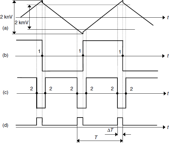
Figure 2.17 Time diagrams of output voltages (a–operation amplifier; b and c–comparators; d–trigger)
The circuit of such a converter and its time diagrams are shown in Figure 2.16 and Figure 2.17 accordingly. The capacitive sensor presented by the two-element parallel equivalent circuit (Rx, Cx) is connected to the operational amplifier's input, with the capacitive negative feedback through the reference capacitor C0. At the operational amplifier's output signal processing, carrying the information about values of leakage capacitance and resistance, two identical comparators are used. Its levels of comparison, formed from the output voltage ±V of the first comparator with the help of the voltage divider, are various and equal accordingly to ±kV and ±kmV (k, m = const). The input voltage of the operational amplifier is equal to ±knV (n = const) and is formed from the same voltage.
The converter is working in an unstable mode. From the analysis of Figure 2.17 it follows that for the moments 1 of the comparator operation the following equality is valid

Its output voltage changes a sign during each half-cycle of oscillation at the moment of 2 (Figure 2.17) equality of voltages on the second comparator's input. The time interval ΔT between comparators' operation is determined from the ratio
Solving Equations (2.41) and (2.42) together we have:
If we take into account that Cx = Cnom ± ΔC, where ΔC is the change of sensor's capacitance under measurand influence and also C0 = Cnom, we have:
where e1 = n/(1 − m); e2 = (1 − 2n)/n are the dimensionless constant factors, whose stability is determined by the stability of the divider's division factors. At m = 2n and ΔC/Cnom = 0, T/2ΔT = 1.
Intervals ΔT and T are formed by the trigger. The measurement of these intervals and calculation of its ratio is realized by the microcontroller.
Thus, the described circuit provides the full independence of conversion results on values Rleackage at rather simple circuit realization. The main error of the transformation does not exceed 0.2%, the conversion time is not more than 10−2 s.
The capacitance-to-period converter for pressure sensors is described in the paper [84]. This transducer is based on a capacitance ratio to the frequency ratio conversion in order to procure a high level of self-compensation for temperature drifts and nonlinearity. The equation of the period is:
where
and If is the leakage current; Cs is the stray capacitance; τd = τ1 + τ2 ≈ 4Δt is the offset. As the universal period meter and different ceramic capacitors have evaluated the converter response with a good resolution (0.01% of the measured value).
The system, which combines passive telemetry with a pressure measuring system, is based on a capacitive type the pressure sensor and ASIC chip, which converts capacitance variations into frequency, is described in [85,86]. The output frequency (up to 160 kHz at 0 mmHg) can be calculated as:
This equation implies that the output frequency is independent of supply voltage and dependent on temperature through the mobility term in k and the threshold voltage Vt. The bias voltage Vbias is chosen to be equal to the bandgap reference voltage produced from the previous stage and is thus considered independent of voltage and temperature variations.
The pressure measuring subsystem consists of a capacitive type pressure sensor and a C/F converter integrated circuit to immediately convert capacitance into the electrical signal. The C/F chip includes the internal voltage regulation and a current-mode comparator, which improves the stability of the output frequency. The C/F dice takes up 1.44 mm2.
The conversion of non-electrical parameters to frequency can also be based on the use of inductive sensors according to one of the following ways: (1) according to the sensor's inductance the frequency of the LC-generator is determined; (2) the sensor is connected to the bridge circuits, balanced by the measurement of the voltage frequency applied to the bridge; (3) the inductance sensor is connected to the selective RL-circuit of the self-oscillator. Today microelectronics and microsystems give us the possibility to realize the smart sensor microsystem including the integrated electrodeposited flat coil and the interface circuit on the same substrate.
Summary
All the described VFC converters share many properties. They have a similar configuration to the integrator, analog switches and the comparator. Many of them can be integrated to smart sensors in order to produce further conversion in the quasi-digital domain instead of the analog domain.
As considered earlier, modern CAD tools contain the microcontroller core and peripheral devices as well as voltage-to-frequency converters. So, for example, the Mentor Graphic CAD tool includes different kinds of VFCs such as AD537/650/652, the CAD tool from Protel includes many library cells of different Burr–Brown's VFCs. The realization of other converters, for example, the capacitance or the resistance-to-frequency are not technological problems for single-chip implementation. All this makes the transition from the analog signal domain to the quasi-digital (frequency-time) domain easy enough.