
7
DIGITAL OUTPUT SMART SENSORS WITH SOFTWARE-CONTROLLED PERFORMANCES AND FUNCTIONAL CAPABILITIES
Digital systems are being ever-increasingly used for measurement and control applications. However, all the variables in the ‘real world’ which sensors are used to measure (such as temperature, pressure, flow or light intensity) are analog in their physical nature: an element is therefore always needed to link the analog environment to the digital system. This usually also means that signals from sensors must be appropriately modified, so as to be made suitable for conversion into a digital data format.
The interface from the analog domain to the digital domain can be a mystifying design problem. The hardware design and the software must operate together to produce a complete, usable design. It is especially true for the smart sensor design. Here the hardware and the software are needed to implement the bridge between the system analog signals and the digital signals.
The use of frequency-to-code converters based on the so-called program-oriented conversion methods (PCM) in combination with frequency output sensors and transducers of electric and non-electric quantities by the creation of smart sensors with embedded microcontrollers was considered earlier (Figures 1.2, 3.7), and seems to promise a lot. In this case, the conversion error is determined by the sensor's accuracy. The hardware or the chip area can be reduced to the minimum possible (the microcontroller core and peripherals).
Not all conventional conversion algorithms are suitable for use in program-oriented conversion methods. Sometimes it is necessary to modify the algorithm or to create in essence a new one taking into account the corresponding microcontroller's capabilities. The basic feature of program-oriented conversion methods is that the programmable computing power is directly included into a converter as part of a measuring circuit and takes part in conversion, i.e. some transformations in measuring procedures executed in a digital form are included. The transformation of the frequency-to-code converter's structure from the hardware realization to the software essentially changes conversion methods and functional possibilities of such devices. Such program-oriented conversion methods for frequency-time domain parameters were proposed in 1988 for the first time and published in 1989–95 with the aim to minimize the hardware (the chip area) and create small-sized, highly reliable smart sensors and sensor microsystems which have minimum power consumption, high metrological performances and self-adapting capabilities.
A definition of the program-oriented conversion method was given in [135]: A PCM is the processor algorithm of measurement, incarnated in the functional-logic structure of a computer or a microcontroller through the software.
For program realization of conversion methods all elementary measuring procedures of the processor algorithm are carried out by the program and the measuring circuit is realized at a virtual level inside the functional-logic architecture of the reprogrammable computing capacity. Due to the dualism of realization of elementary operations of the measuring procedure inherent in the architecture of modern microcontrollers, the realization of a whole class of PCMs, which are based only on one conversion method, for example, the ratiometric counting method, is possible. Thus, such a method of measurement represents the basis for all possible PCMs. In fact, the PCM is a program model of hardware realization of a measuring circuit and can be unequivocally set up by the concrete basis and the processor algorithm of its realization.
Depending on the program realization there are two types of program model construction: compilating and interpreting. PCMs are procedures with complex functional-logic structures containing critical time-dependent pieces of programs so that their algorithms, according to the specified classification are constructed according to the compilating way of the program realization by which for every PCM the specific program is realized.
The variety of PCMs demands further development of their classification, taking into account detailed attributes for the ordering of existing and the development of new PCMs, for example, as in the work [99] concerning methods of measurement used in frequency-to-code converters based on a hardwired logic.
It is possible to characterize a PCM by certain generalizing attributes, which are peculiar to each PCM based on any basis and method of measurement. According to the program realization of frequency and time references, PCMs can be subdivided into methods:
- with program delays formed
- with time intervals formed by means of built-in timer/counters (T/C).
Depending on the realization of the events counting algorithm, PCMs can be subdivided into methods:
- with counting on polling (synchronous or asynchronous)
- with counting on interruptions (single-level or multilevel)
- with counting with the help of the timer/counters.
7.1 Program-Oriented Conversion Methods Based on Ratiometric Counting Technique
Let's consider the realization of the program-oriented method for the frequency-to-code conversion based on the ratiometric counting technique. Algorithms of measurements, based on this method, demand a high multisequencing degree of elementary measuring procedures of processor algorithms. For a long time this was a constraint on such PCMs on the basis of traditional microprocessor systems. However, modern microcontrollers have well-developed functional-logic architectures and instruction sets focused on an effective realization of input/output procedures, providing, thus, a multiway PCM realization based on the ratiometric counting method. High efficiency of PCMs by design should be provided by careful analysis of processor algorithms' structures, the use of resources of microcontrollers' architectures and correct determination of the software part, which requires the optimization.
In the design, the PCM can be represented as a set of software components of a high-level hierarchy. The latter, in its turn, consists of elementary low-level software components. It is an elementary procedure realized at the virtual level. So, for PCM realization based on the ratiometric counting method a concurrent execution of four elementary procedures is necessary: the first gate time T01 forming; the second gate time T02 forming, the wavefront and the wavetail of which are strictly synchronized with pulses of the input frequency fx; the counting of reference f0 and measurand fx frequencies (Figure 5.2).
The decomposition of the PCM into elementary measuring procedures and variants of its possible software realizations are shown in Table 7.1.
In order to generate the set of possible PCM realizations, it is expedient to analyse all possible realizations of these operations, given by the functional-logic opportunities of microcontrollers.
The first gate time T01 can be formed by a built-in timer/counter or by a software time delay constructed with the help of nested iterations and the combination of precisely trimmed delays of smaller duration.
Ranges of possible delays by the timer/counter for microcontrollers of MCS (Intel) and MSP430 (Texas Instruments) families are adduced in Table 7.2. Here fosc is the frequency of the crystal oscillator; n is the number of bits of the timer/counter. Delays of greater duration can be realized by construction of cycles with timer/counter reloads. By using a timer/counter for the forming of time intervals, there is an error Δtint caused by the time of instruction execution necessary for the control transfer to the interrupt vector of the internal interruption and the ‘stop’ instruction for a timer/counter. It is a systematic error and can be corrected.
Table 7.1 Variants of possible software realizations for measuring procedures

Table 7.2 Ranges for possible delays for timers/counters

From time delays forming, the minimum possible duration is determined by the minimum microcontroller's instruction execution time. As a rule, it is the NOP (no operation) instruction. Its execution time is equal as a rule to one machine cycle. The inefficient use of microcontroller's resources is the main disadvantage of programming time delay forming. The forming of second gate time T02 is often carried out by means of the logic analysis of events. The counting of pulses fx and f0 can be realized by one of three possible ways: by software asynchronous polling; by interruptions and with the help of T/C. Each of these ways brings the restrictions connected with additional errors of measurement, which must be taken into account by the metrological analysis of the developed PCM, and, whenever it is possible, must be corrected.
The realization of a PCM with counting of events with the help of program asynchronous polling becomes simpler due to the microcontroller's conditional jump instruction according to the presence of a high logic level ‘1’ in the microcontroller's inputs. However, in order to prevent pulse losses of the input frequency fx as well as a false reading, the maximum converted frequency and the pulse τx duration should be chosen from the following system of inequalities:
where Tx max is the period of the converted frequency; τcycle is the duration of the machine cycle; n is the number of machine cycles necessary for realization of the polling program; τJump is the execution time for the conditional jump instruction according to the presence of a high logic level ‘1’ in the microcontroller's inputs.
The maximum converted frequency for a PCM with counting of events by interruptions is limited by the ratio
where TINT is the execution time of the interrupt subroutine. Thus, it is necessary to provide the presence of an active level of a signal of the external interruption during the time:
where n is the number determined for each type of microcontroller.
The maximum converted frequency for a PCM with the counting of events by means of built-in timer/counters is limited only by electronic components, i.e. by the maximum frequency, which can be counted by the timers/counters. The minimum duration of a signal on the timer/counter inputs is regulated by specifications on the microcontroller. Such a PCM allows frequency-to-code converters with the greatest possible converted frequency fx and the minimum quantization error. Maximum possible frequencies on timer/counter's inputs for various microcontroller families are adduced in Table 7.3.
The minimum converted frequency fx min is practically unlimited and determined by the maximum virtual counter capacity, which is determined in its turn, by the capacity of all free general-purpose registers and all accessible sizes of the internal microcontroller's RAM:
where N2 max = 2k = const; k is the capacity of the virtual counter, realized in general-purpose registers and/or in the RAM for the reference frequency pulse f0 calculation. The graph of the function fx min (f0, N2) is shown in Figure 7.1.
The use of microcontrollers with an architecture containing two or more built-in timer/counters, for example, microcontrollers 8X52, 8XC5X, 8XL5X, 8XC51FX, 8XL51FX and 8XC51GB (Intel) expands the high range of converted frequencies for all specified advantages of the PCM.
If a third timer/counter is used for forming the reference time interval T01, converter speed will be increased. Thus, quasi-pipeline data processing can be realized. One more advantage of the microcontroller architecture with three timer/counters is an opportunity to use the third timer/counter in the software-controlled frequency output Clock-Out mode. In this mode, the meander with the programmed frequency of pulses is generated on the T2 (P1.0) output. This mode is useful for forming the reference frequency f0 pulses. In this case, it is not necessary to use the preliminary frequency divider in the converter. The output frequency on the T2 depends on the frequency of the crystal oscillator and the number reloaded into the timer from registers RCAP2H, RCAP2L and can be calculated according to the formula:
Table 7.3 Maximum possible frequency on timer/counters inputs for various microcontroller families
| Type of μK | Maximum frequency on T/C input |
| MCS-51 | fosc/24 |
| MCS-251 | fosc/8 |
| MCS–96/196 | fosc/4 |
| MSP430C33x (for MCLK) | 3.8 MHz |
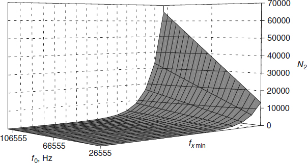
Figure 7.1 Graph of function fx min (f0, N2)
The increase of the reference frequency f0 up to Fclc/4 is possible due to the PCM realization based on microcontrollers containing a programmable counter array (PCA). It is a good internal device for measurement of the period, the pulse duration, phases differences, etc., in five channels at the same time. Thus, there is a possibility to create converters with increased accuracy due to quantization error reduction.
It is necessary to take into account that not only methodical errors caused by processing algorithm properties, but also the computing capacity built-in to the measuring circuit as well as programming style influence the conversion result. Hence, in order to reduce systematic and random errors of the measurement, it is expedient to build the PCM algorithm in a rational way from the metrological efficiency point of view, i.e. software optimization with the help of the morphological analysis according to the chosen criteria—the minimum of these components.
According to the metrological analysis, the conversion error includes components caused by software properties that have been written in a low-level computer language (assembler). This error can be minimized by using an optimal PCM.
The optimal operator is determined by the equation
where r2(Akxk, Axk) is the non-identity error, caused by the difference between the measuring algorithm and the actually realized algorithm by the software; {A}accept is the allowable set of operators limited by requirements, from which the ![]() is chosen. One of the sine qua non to the class {A}opt of allowable operators is that the number of possible realizations is finite. In the case of the discrete optimal choice of the PCM, the set {A}accept is set up as a final set of known operators with known parameters:
is chosen. One of the sine qua non to the class {A}opt of allowable operators is that the number of possible realizations is finite. In the case of the discrete optimal choice of the PCM, the set {A}accept is set up as a final set of known operators with known parameters:
It is necessary to choose the best variant from them
where ![]() is the required operator.
is the required operator.
Such a task arises by the microcontroller choice as well as at the synthesis of the optimum PCM from the finite number of possible elementary measuring procedures of the processor algorithm.
At the final design stage the value of the algorithmic error with its maximum permissible value Δ2 is compared according to the following rule
The inequality r2 ≥ Δ2 indicates:
- For Equation (7.6)—within the frame of given restrictions the requirement r2 < Δ2 is not valid, inasmuch as the value r2 is characterized by the limited (potential) quality of the PCM. Assuming that
where r1 is the theoretical error, we conclude that it is necessary to increase the value Γ, i.e. the reconsideration of given data.
- For Equation case (7.8)—it is necessary to chose another microcontroller or to create the PCM based on another basis (Equation 7.6), for example, based on the method of the dependent count.
Recommendations on the basis of the morphological analysis for designing the minimum PCM hardware for frequency-to-code converters on the basis of a microcontroller, are based on the main metrological features such as:
- The open character of frequency-to-code converter functionalities.
- An opportunity to exchange accuracy to speed and conversely (self-adapting capabilities) or extension of a measuring range up to high frequencies.
- Practically unlimited range of low and infralow converted frequencies.
- A high degree of multisequencing operations of the conversion algorithm.
- The essential complication of smart processor algorithms (adaptation, correction, calibration, self-diagnostics; statistical processing etc.).
- The growth of the relative density and complication of the structure of the methodical and, first of all, algorithmic component of the error of measurements.
Due to the functional-logical capabilities of modern microcontrollers and dualism of realizations for the main operations of the conversion algorithm, the 10–18 realizations of software components at a high level are possible on average. From set theory, the program-oriented method of conversion can be represented as the union of p disjoint sets N of software realizations of elementary operations of the i-th conversion algorithm:
where S1, S2, S3, …, Sp includes n1, n2, n3, …, np elements accordingly. The determination of a general number of possible conversion methods (the first design stage) for the particular basis and a microcontroller is the combinatory task. For a generation of PCM variants with the help of a choice of necessary combinations from sets S1, S2, S3, …, Sp, it is necessary to combine each choice of elements from the set S1 with each choice of elements from S2, S3, …, Sp. Similarly, each choice of elements from S2, S3, …, Sp should be combined with a choice of elements from S1, S3, …, Sp, from S1, S2, …, Sp and S1, S2, S3, …, Sp−1 accordingly. Therefore the number of elements of the set R* (i.e., the tuple from k elements of the set S*), from which k1 ∈ S1, k2 ∈ S2, k3 ∈ S3, …, kp ∈ Sp is equal to:

where q is the number of incompatible realizations of the PCM, i.e. operations that cannot be executed within the frame of a certain microcontroller's architecture simultaneously. So for example, the pulse counting of f0 and fx can be realized with the help of the timer/counters, however, in the frame of a one-timer/counter microcontroller's architecture it is impossible to carry out these two operations simultaneously.
For PCM realization on the basis of the ratiometric counting technique it is necessary, as described earlier, to realize three elementary procedures: to form the first gate time T01 and count pulses of the unknown fx and reference f0 frequencies. Then, the general number of alternative, possible in principle, variants of the PCM in view of incompatible operations for the one-timer microcontroller's architecture (one timer/counter and one input of external interruptions), is determined as:
For microcontrollers of the base configuration with two timer/counters:
and for microcontrollers of the extended configuration with three timer/counters:
The algorithmic structure of the PCM in many respects depends on the used basis (conversion method) and the microcontroller type. The choice of the optimum PCM, from the metrological criterion of the efficiency point of view, among all varieties of allowable realizations, is not a trivial task. The successful choice of the required PCM in many respects is determined by designer experience. The choice of the optimum discrete PCM is carried out with the help of the design methodology for reusable software components of smart sensors [136], which will be described in the following section.
7.2 Design Methodology for Program-Oriented Conversion Methods
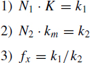
The discrete choice of optimum alternative variants of the PCM in the finite set of allowable realizations represents a characteristic task of vector synthesis (optimization). By a discrete choice, the set of strongly admissible systems forms the given discrete finite set Msa of points in the n-dimensional Euclidean space Rm of the characteristic. The task of synthesis consists in the choice of such a point a* ∈ Msa from this set, which has the best value of the vector of characteristic
that is, the best in the sense of the chosen criterion of preference, and satisfying all sets D = {C, Os, QV, Ok} of initial data, where C = {C1, …, Cp} is the set of conditions; Os = {Os1, …, Osq} is the set of restrictions on the structure and parameters of the designed frequency-to-code converter (the hard constraint on the used microcontroller type and the conversion method); QV = < k1, …, km > is the structure of the vector of characteristic of the PCM; Ok = Ok1, …, Okr is the set of restrictions, imposed on parameters of a quality [137].
From all strictly allowable PCMs, we shall choose the optimum PCM that has the best value of the vector of characteristic K. Hence, one of the major procedures of vector synthesis is the choice of the optimization criterion K.
For further description of the design methodology of optimum PCMs, it is necessary to take advantage of following definitions [137]:
Definition 1. The system S satisfying the set {C, Os} of the initial data is referred to as allowable.
Definition 2. The allowable system satisfying the set of restrictions Ok is referred to as strictly allowable, i.e. satisfying the whole set D = {C, Os, VQ, Ok}.
In general, the processor algorithm of the PCM is estimated by some set of parameters of efficiency
and it is usual that |K| = m > 1.
For successful synthesis of the optimum PCM, it is necessary to choose such a subset ![]() ∈ K, which most fully characterizes various properties of the frequency-to-code converter in view of its application (smart sensor features) and requirements. On the other hand, for simplification of the synthesis of the frequency-to-code converter based on the PCM, it is desirable to limit the subset
∈ K, which most fully characterizes various properties of the frequency-to-code converter in view of its application (smart sensor features) and requirements. On the other hand, for simplification of the synthesis of the frequency-to-code converter based on the PCM, it is desirable to limit the subset ![]() whenever possible by parameters that estimate in the greatest degree the ability of the device to carry out its functions from the application point of view.
whenever possible by parameters that estimate in the greatest degree the ability of the device to carry out its functions from the application point of view.
As the structure of the frequency-to-code converter based on a certain microcontroller core is fixed (rigid restrictions on the structure), it is not necessary to compare various PCMs according to the complexity S. On the other hand, on the basis of the microcontroller type and conversion method Vn PCM variants can be realized according to Equation (7.12); important specific and essential characteristics by comparison of alternative PCM variants are the quantization error δ(%) and the maximum possible converted frequency fx max (Hz).
As the PCM supposes various algorithms of realization {Aaccept} from the set of allowable variants of the realization Ma, another essential characteristic by PCM comparison can be the memory sizes VROM (byte) and the power consumption P. These last two parameters are rather essential for one-chip smart sensor realization.
With provision for the negative ingredient for parameters of quality, the optimization criterion can be written, for example, as follows:
at Tij < Tijaccept, where Tijaccept is the allowable conversion time; {Bij} is the set of allowable variants for the ith PCM, and δij, Txij, VROMij, Pij are factors of the jth allowable variant of the ith PCM; Txij = 1/fxij.
For the forming of the integrated parameter of the quality Ki, it is expedient to take advantage of the weight-average geometrical complex parameter, which is written as follows
where ![]() is the minimum value of appropriate parameters of quality on all allowable variants of the PCM; νi is the normalized weight factor of proportionality for appropriate parameters, and
is the minimum value of appropriate parameters of quality on all allowable variants of the PCM; νi is the normalized weight factor of proportionality for appropriate parameters, and
Then the integrated criterion of the PCM efficiency can be submitted as a multiplicate loss function:

where δi min, Txi min, VROMi min, Pi min are the minimum values of appropriate parameters of quality on all allowable variants of the ith PCM; νiδ, νiT, νiROM, νiP are the weight factors of priority for appropriate parameters of quality; Txi is the period of the converted frequency. Thus
and
In Equation (7.21), instead of fxi max the value Txi min is used to reduce this parameter of quality to the standard kind.
The criterion function according to Equation (7.21) characterizes the set of effective solutions well enough. In other words, the maximization of this function gives the effective solution for the initial multicriterial task. In the contrast to other methods using weight factors, these factors are well interpreted in the given scalarization. They depend on the desirable value of criterion: if the desirable level is closer to the optimum value, the criterion is more important and the weight factor has the greater value. In its turn, the allowable variant of the PCM realization is that for which ![]() is true. The optimal variant from all those allowable will be the variant that has the maximal value Kij, and Kij max = 1. Thus, Kij is the non-linear function of normalized dimensionless parameters {ki}. Depending on the weight factors of parameters of quality, which are included in the integrated criterion Kij, it is possible to choose a PCM, optimizing it according to one of the following parameters: the minimal period of converted frequencies, the quantization error, the ROM memory size, the power consumption, etc.
is true. The optimal variant from all those allowable will be the variant that has the maximal value Kij, and Kij max = 1. Thus, Kij is the non-linear function of normalized dimensionless parameters {ki}. Depending on the weight factors of parameters of quality, which are included in the integrated criterion Kij, it is possible to choose a PCM, optimizing it according to one of the following parameters: the minimal period of converted frequencies, the quantization error, the ROM memory size, the power consumption, etc.
Equation (7.18), in view of the criterion resulting function (Equation 7.21), represents a non-linear discrete task of optimum designing.
As follows from different references devoted to methods of vector optimization, a reliable solution of the synthesis task can be obtained only as a result of the combination of various optimality criteria, in particular, an unconditional and conditional criterion of preference.
In view of the above, it is possible to allocate the following stages of the discrete choice of the optimal PCM for frequency–time parameters:
- The analysis of the PCM's algorithm and restrictions on its realization, the forming and ordering of the set Msa of strictly allowable PCMs (catalogue compiling of alternative, possible in principle, variants of software realizations).
- The set partition Msa into the set of worse Mw and non-worse Mnw systems with the help of the unconditional criterion of preference (finding of the left lower boundary).
- The use of the conditional criterion of preference for searching of the optimum PCM in the set Mnw when the set of non-worse systems is nondegenerated.
- The analysis of synthesis results on stability and definiteness.
Further, it is expedient to provide remarks and practical recommendations for the execution of these design stages.
The preparative stage. Before this synthesis stage, it is necessary to choose the PCM basis (as considered above, it is expedient to choose any of the advanced methods for the frequency-to-code conversion, for example, the ratiometric counting method) and the type of the embedded microcontroller or the microcontroller core. In general, the task of microcontroller choice for the frequency-to-code converter and optimization estimations of functional-logic features of the microcontroller architecture, are tasks of the structural synthesis.
The set of given microcontrollers m is the open set, which is extended by new microcontrollers or standard libraries of cells in CAD tools. Therefore, the optimal microcontroller for the use in frequency-to-code converters is the microcontroller (or the microcontroller core) that provides PCM realization within the frame of given restrictions at minimum expense:
where ε is the maximum number of different microcontrollers.
Stage 1. In order to obtain the solution closest to the optimal, the PCM must be decomposed into a number of elementary procedures by the method of decomposition: forming the gate time T01, the pulse counting of fx, f0 etc., and then the synthesis method through the analysis of allowable variants ![]() is used.
is used.
The enumeration of possible alternative variants of the PCM in the finite set Msa depends on the discrete choice task. Because the set Msa of the PCM is foreseeable and finite (NA = 10–18) the algorithm of full enumeration and the exclusion of unpromising variants based on the method of the consecutive analysis of variants is used in order to find the optimum PCM from a small, known number of variants. In order to use this method it is necessary to compose a catalogue of all PCM variants. The common number of alternative variants ![]() is determined according to Equations (7.12–7.15), and their generation is carried out according to Equation (7.11). In order not to miss alternatives, the set Msa should be preliminary ordered.
is determined according to Equations (7.12–7.15), and their generation is carried out according to Equation (7.11). In order not to miss alternatives, the set Msa should be preliminary ordered.
The morphological matrix is frequently used for the construction of a catalogue of possible program-oriented conversion methods from the high-level software components. However, this matrix does not reflect the specificity of decomposition of program-oriented methods. For this aim, it is more convenient to take advantage of the morphological tensor ωA(a, b, c), which is created based on the functional-logical analysis of developed program-oriented methods. Methods of the software realization of the three basic elementary procedures of the algorithm (Table 7.1) are selected as the most important criteria. In this tensor, the maximum value of the index a is determined by the number of possible realizations of the pulse count fx, b by the number of realizations of the pulse count f0, and c by the number of possible variants of forming the gate time T01. The numerical values of indexes and realizations of elementary operations, appropriate to these values, are shown in Table 7.4.
The tensor's element Xabc is a Boolean variable. Its value is equal to ‘1’ by the choice of the program-oriented conversion method, otherwise it is equal to ‘0’. The condition of alternatives can be expressed as follows:

Further description of the technique for a discrete choice of optimum program-oriented conversion methods is provided by an example of the sensor microsystems synthesis based on widespread MCS-51 (Intel) microcontroller families. Let the microcontroller contain only one timer/counter and be able to service one interrupt from one external source.
Table 7.4 Numerical values of indexes and elementary operations realizations

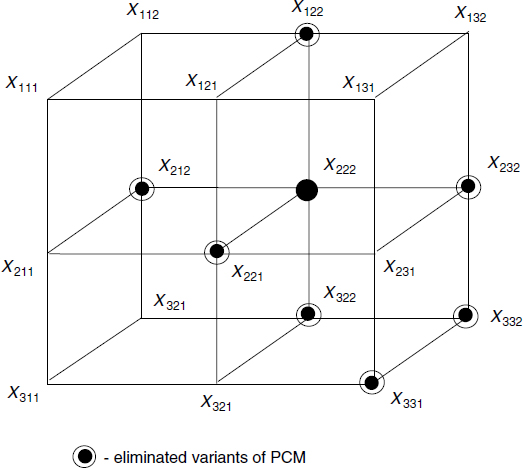
Figure 7.2 Morphological block of possible alternative variants of a PCM
The morphological block of possible alternative variants of program-oriented conversion methods, from which incompatible q variants for the given microcontroller operations are eliminated, is shown in Figure 7.2.
The operation can be presented by the indexes ratio of tensor's elements:
Further dimension reduction of morphological space is carried out by the argumentation of the integrated criterion of efficiency.
Stage 2. As the set ![]() of strictly allowable PCMs, generated according to Equations (7.12–7.15) is nondegenerated and finite (1 < I < ∞), the following theorem [137] is valid:
of strictly allowable PCMs, generated according to Equations (7.12–7.15) is nondegenerated and finite (1 < I < ∞), the following theorem [137] is valid:
Theorem. If Msa is a finite set, the set of non-worse systems Mnw is the nonempty set.
In order to simplify the Mnw determination, it is expedient to exclude minor parameters of quality from the integrated criterion of efficiency at the initial stage. First of all, these are VROMij and Pij (Equation (7.18)) as they do not influence the PCM metrological efficiency. Their maximum values are determined at the preparative stage of the synthesis and limited by functional-logic features of the chosen microcontroller. Thus, the synthesis task of the optimum PCM has been reduced to the choice of the optimum PCM according to the maximum of a metrological criterion of efficiency, determined only by two parameters of quality: δij and Txij.
The results of the analysis of alternative PCMs according to the metrological criterion of efficiency are shown in Table 7.5. The variants distinguished only by the index c, can be joined, as they have the same values δ and fx(Tx). These values do not depend on the method for forming the gate time T01, because the reference time interval is always formed with the accuracy determined by the accuracy of a quartz generator of the microcontroller.
For the set partition of strongly allowable variants of the PCM into the set of worse and non-worse PCM with the help of the unconditional criterion of preference, it is expedient to take advantage of the method of rectangles [137]. In comparison to other methods for finding the left lower boundary, the opportunity to lose non-worse PCMs, including the optimal one is excluded. Besides, the algorithm of the equivalent analytical procedure of this method can be easily formalized and is suitable for the realization on a PC, as software for CAD tools.
Stages for the left lower boundary determination are shown in Figure 7.3. In this case it consists only of two points: X231 and X321. As the left lower boundary is a special case of the optimum surface (m = 2), the following property is valid for it: on the whole expansion of the left lower boundary the dependence δ = f (Tx min) and consequently, the Tx min = ϕ(δ), has the monotonely decreasing character.
Table 7.5 Results of analysis of alternative PCM (at T01 = 0.25 s, fclc = 6 MHz)


Figure 7.3 Stages of left lower boundary determination
It is now necessary to take advantage of the conditional criterion of preference in order to finish the synthesis procedure.
Stage 3. Taking into account excluded minor parameters of quality the resulting criterion function will be:

and the formulation of the synthesis task can be written in the following way

where Kim is the value of the factor Ki that is the maximum possible. Because the nondegenerated set Mnw contains only two PCMs, one of which has the least value of the quantization error δi min, and the other the minimum value of the converted period Txi min, the integrated quality factor for the variant X231 is reduced into the formula
and for the variant X321 into the formula
A more optimum variant is X321 with the values Kij = 0.5 against 0.41 accordingly by equivalent requirements for the PCM accuracy and speed (weight factors of priority for quality indexes are equal, i.e. νiδ = νiT = 0.5). Plots of functions (7.29) and (7.30) with allowance for relations νiδ + νiT = 1 are shown in Figure 7.4. These dependencies can be used during the synthesis of the PCM, facilitating a choice of the PCM according to requirements of speed or accuracy.
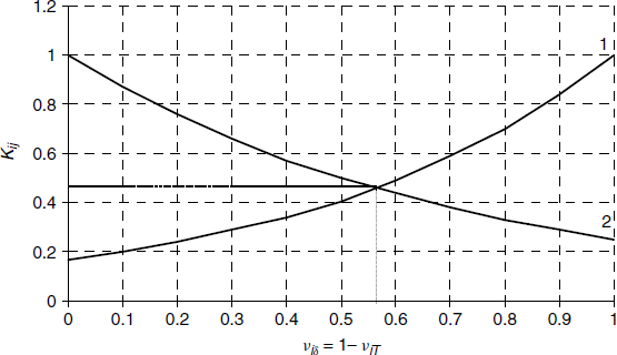
Figure 7.4 Graph of function Kij = f (νiδ) (1) and Kij = f (νiT) (2)
Stage 4. It is obvious that the PCM synthesis is completed if the following two conditions are valid:
- The solution obtained as a result of the synthesis, is determined enough and precise, i.e. the PCM class, satisfying all formulated initial data, including the optimal criterion, is not too wide.
- The received solution (class PCM) is steady enough by the variation in reasonable limits of initial data, including preference relations.
Really, the nondegenerated set Mnw contains two PCMs and the result of the synthesis will be similar using the criterion of efficiency (Equation (7.21)) instead of (Equation (7.27)) as well as by taking into consideration variants distinguished by gate time forming the T01.
The given technique of the discrete PCM choice is applicable also to microcontroller architectures containing two or more built-in timer/counters. Thus, the generation of possible alternative variants of the PCM is made according to Equations (7.14), (7.15) accordingly. The morphological block of possible PCM variants will be similar to that shown in Figure 7.2. It is necessary to eliminate only one variant, satisfying the following condition
i.e. the variant X222 in case of the microcontroller architecture with two built-in timer/counters. In the case of improved architectures with three or more timer/counters, there are no variants of the PCM with incompatible operations. In the first case, the use of the unconditional criterion of preference at the second synthesis stage results into the unique solution X221 (the set Mnw is degenerated), in the second case, into the solution X221/222. Thus, based on the conditional criterion of preference according to the resulting criterion function (Equation (7.21)), preference should be given to the variant X222, as this requires less program memory size for its realization.
Thus, the task of the choice of the optimal PCM can be reduced in general to the non-linear discrete task of optimal designing. This technique covers almost all functional-logic architectures of modern microcontrollers, suitable for PCM realization based on classical and advanced methods of the frequency (period)-to-code conversion for its use in different smart sensors. The technique is well formalized and allows algorithms of all stages of the morphological synthesis, thus providing an opportunity for automatization of procedures of the discrete choice of PCM and the creation on this basis of appropriate software for modern CAD tools [138].
7.2.1 Example
The control flow chart of an optimum PCM, with the microcontroller family MCS-51 (Intel), is shown in Figure 7.5 and its software in Figure 7.6 respectively. As microcontrollers of this family contain two–three 16-bit timer/counters, it is expedient to realize the PCM in the following way. Pulses of frequencies fx and f0 are counted simultaneously by two timer/counters, and the T01 form with the help of the software delay or by the third timer/counter (if it is in the microcontroller). Timer/counters overflows cause internal interruptions, which are counted by virtual counters based on general-purpose registers R0 and R. Thus, the greatest possible converted frequency and the minimum quantization error are reached. The reference frequency f0 is formed by the frequency divider. The gate time T02 is formed with the help of two level interruptions on inputs INT0, INT1.

Figure 7.5 Control flow chart of optimal PCM based on MCS-51 microcontrollers
The frequency-to-code converter works as follows. At the beginning of the process, operation modes for T/C0, T/C1 are chosen and the priority of external interruptions is established: for INT1/0–the maximum; for T/C0/1–the lowest (blocks 1,2). Then types of interruptions (on the wavetail) are programmed (block 3), all registers of virtual counters of N1, N2 and the user's bit F0 in the fifth bit PSW.5 are reset (block 4). Then the timer/counter T/C0 for pulse fx count is started and the interruption from INT0 is enabled (blocks 5,6) After that, the time delay T01 = 1 s (block 7) is formed using software. When this time finishes, the T/C0 is stopped (block 8), the interruption from INT1 is enabled (the block 9) and the program waits for the last pulse fx, to finish a measuring cycle (block 10). Then the subroutine for the frequency fx calculation (block 11) is executed and the measuring cycle is repeated again.


Figure 7.6 Program for PCM realization
The interruption subroutine from INT0 starts T/C1 for counting pulses of the reference frequency f0 and forbids the interruption on the input INT0. In its turn, the interruption subroutine from INT1 stops T/C1, forbids the interruption INT1 and sets up the user bit in ‘1’. Interruption subroutines from the timer/counters overflow increment virtual counters.
The PCM used in such a converter has a high degree of the elementary operations concurrency of the measuring algorithm. The high conversion frequency range is limited only by the greatest possible value of frequency, which the timer/counters can count.
7.3 Adaptive PCM with Increased Speed
For PCM realization of frequency–time parameters of signals with the pulse counting of frequencies fx by interruptions and forming the gate time T01 by the method of the nested iteration and a combination of precisely trimmed delays of the smaller duration, there is a problem connected with T01 increasing because of the summation of times of external τINT and internal τTC interruption subroutine executions with the gate time T01. In general, the total conversion time without taking into account mathematical processing, is determined according to the following formula
Taking into account the equation for N1, after transformations we have:
where N1 is the number of pulses fx, arriving at the interruption input during the time T01; Nm is the number of internal interruptions on timer/counter overflows. For the high frequency range, the value τdelay becomes more or equal to T01, thus increasing the conversion time and the dynamic error.
The use of adaptive PCMs avoids the loss of speed. By the algorithmic adaptation, the structure of the PCM's processor algorithm is purposefully varied during the frequency-to-code conversion. In general, the controlling factor can be presented as
where A are the factors, which help to change the algorithmic structure.
As the algorithmic structure of the PCM is characterized by the stable conjunction of elementary procedures, the use of such an adaptation optimizes the structure of the processor algorithm. The task of adaptation can be formalized by the following way:
where Q is the minimum criterion (in this case, the minimum Tconversion); EA is the set of allowable algorithmic structures A; A* is the optimal algorithm.
With the aim of time τINT compensation, which can be calculated according to the formula
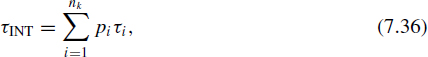
where pi is the instruction with the execution time τi; nk is the number of instructions of the interruption subroutine, the time delay program forming the gate time T01 is modified during the frequency-to-code conversion. Thus, the interruption subroutine for external interruptions from pulses fx should contain at least one decrement instruction for the microcontroller's register DEC <reg>. The number written in this general-purpose register is the controlled loop variable, realizing the time delay equal to the time of the subroutine execution. In its turn, this cycle is included in the program body forming the gate time T01. With such a structure of the PCM's algorithm, each subroutine execution automatically reduces the time T01 for the τINT value and the gate time T01 remains constant in all ranges of converted frequencies. The PCM adaptation is realized in parallel to the frequency-to-code conversion on the basis of the current information about the frequency fx, without the use of the aprioristic information about the measurand. The graph of the function Tconversion = ϕ(fx) for the conventional and adapting PCM is shown in Figure 7.7. The piece of the program forming the gate time T01, which meets the requirements of adaptation is shown in Figure 7.8. Thus, the looping time is τcycle = τINT.
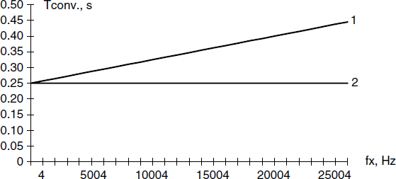
Figure 7.7 Graph of function Tconversion = φ(fx) for conventional (1) and adapting (2) PCMs
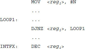
Figure 7.8 Piece of program forming gate time T01
Apart from the compensation of the subroutine execution times of the interruptions processing, the PCM algorithmic adaptation modifies interrupt vectors during the frequency-to-code conversion. This property of the adaptive PCM allows the realization of multifunctional converters, functioning according to complex measuring processor algorithms in conditions of a limited number of interrupt vectors.
In this case, instead of the unconditional jump instruction to the address of the interruptions subroutine, required by the protocol of the interruptions processing, the indirect jump instruction to the address of the virtual interrupt vector is situated. According to the required algorithm, the interruptions subroutine modifies the virtual interrupt vector at the end of the interrupt processing. Due to this, the following interrupt initializes the execution of another subroutine, which in its turn, can modify the virtual interrupt vector again, initializing the previous or a new interruptions subroutine and so on.
The method of the PCM adaptation with the use of virtual interrupt vectors is effective for both external (hardware) and internal (software) interruptions. Such a protocol of the interruptions service is expedient to use, for example, for PCMs of phase shifts-to-code converters.
In multifunctional converters based on adaptive PCMs, the established set of measuring functions {F Mi} is executed with the help of {Pni} interruptions subroutines due to which, the set of algorithms {AMi} is realized. The concrete algorithm is chosen on the basis of the current information about the measurand, conditions of measurements, requirements and restrictions.
The use of the adaptive PCM for frequency–time parameters of electrical signals with the pulse counting fx by interruption, allows an increase in the conversion speed (without taking into account the time of the result processing) by approximately two times and realizes multipurpose measuring algorithms in conditions of a limited number of interrupt vectors in the microcontroller.
7.4 Error Analysis of PCM
The analysis of the total conversion error is necessary, for estimation of dominant components bringing the greatest contribution to the resulting error, for revealing specific errors inherent only to program-oriented conversion methods for the frequency-to-code conversion and also for the local optimization task definition, the solution of which reduces these dominant components.
The general structure of the conversion error for the frequency-to-code converter based on the ratiometric counting method is shown in Figure 7.9. For analytical equations describing errors of synthesized optimum PCMs, it is necessary to investigate separate components of this error. In view of the features of the algorithm execution, it is expedient to choose a structure of the total error, which permits its factor-to-factor research. For this aim, having calculated the total differential of Equation (5.4) and having finite increments and relative units, we obtain the relative conversion error, which can be submitted as:
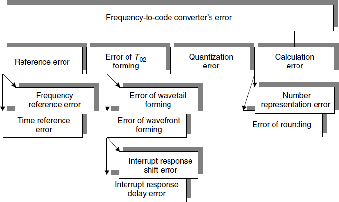
Figure 7.9 General structure of conversion error
where Δf0/f0 is the relative error of reference; ΔN1/fx · T01 and ΔN2/f0 · T01 are the relative quantization errors. The first component of the quantization error is minimized by the choice of conversion time, multiple to the period of converted frequencies and the use of f0 = fmax for the given microcontroller. The conversion error will thus be equal to
Frequently, the second component quantization error is determined according to the formula for engineering calculations (Equation (5.7)). A more exact mathematical model (Equation (5.10)) of the given component has been described earlier in Chapter 5.
7.4.1 Reference error
The reference error is represented by two components: the time reference error by the forming of the gate time T01 with the help of the software delay and the frequency reference error f0, by the frequency division or generation with the help of the timer/counter, working in the mode of the programmable frequency output ‘Clock-Out’. The reference error is practically identified with the error caused by instability of a reference-frequency source (a quartz generator), inherent to any microcontroller. Change of quartz generator parameters is determined by the influence of a large number of random factors and consequently is a random variable distributed according to the central limiting theorem under the normal distribution law.
The maximum accuracy of frequency-to-code conversion is determined by the frequency stability of the built-in quartz-crystal generator. The system clock generator is a ‘measurement standard’ in these converters.
The temperature instability of the quartz-crystal generator is one of the main components of the parametric instability, which has the greatest density in comparison with other components. As known, the frequency deviation of the non-temperature-compensated crystal oscillator from the nominal due to the temperature change is (1–50) × 10−6 in the temperature interval (−55– + 125 °C) and in the frequency range 5–50 MHz. In its turn, modern program-oriented methods of frequency-to-code conversion are able to obtain the quantization error, commensurable with the temperature instability of the references. Therefore, knowledge about the more exact value of the measurement standard uncertainty is a necessary condition for designing accurate frequency-to-code converters for smart frequency–time-domain sensors.
To obtain the exact value of the reference accuracy is possible only by experiment. Experimental researches of quartz-crystal generators have a large complexity because of considerable amount of time consumed on the temperature characterization. Due to a large scatter, appropriate to the real-temperature characteristics of quartz-crystal generators, the experiment assumes a very important place in the design and manufacture of accurate smart sensors. The aim of this section is to acquaint the reader with the technique of experimental researches of the reference error in order to be able to repeat such experiments for any type of microcontrollers.
The research of quartz-crystal generators in the working temperature interval with the aim to determine the temperature instability of frequency is common for all varieties of quartz generators. The temperature instability of frequency in the whole working temperature interval from tmin up to tmax is determined as [139]:
where fmax and fmin are maximum and minimum values of the generator's frequencies in the working temperature range.
The objectives of the experiment were [140]: (i) to determine the temperature instability of frequency and time references of the embedded microcontroller; (ii) to determine the correlation factor of their errors; (iii) to determine distribution laws for the temperature uncertainty. As an experimental sample the one-chip microcontroller from the MCS-51 (Intel) microcontroller family was selected, because of its very wide distribution due to the usability of its functional-logical architecture.
According to the algorithm of the method used for the frequency-to-code conversion, frequency and time references were realized based on the built-in quartz-crystal generator. The frequency reference was obtained in the following way. The synchronization signal of the internal system clock generator of the microcontroller through the output ALE was applied to the input of the external frequency divider by three. Then the signal fALE/3 was applied to the input of the built-in microcontroller's timers/counters. The 6 MHz resonator RG-05 was used as a quartz-crystal oscillator. The time reference was obtained in the following way. The required time interval was formed with the help of the delay subroutine. This subroutine was realized by the method of nested program cycles and combinations of precisely set up delays with smaller duration. The schematic diagram of the experimental set up is shown in Figure 7.10. For the determination of the temperature instability of frequency the quartz-crystal oscillator was cooled up to a temperature equal to the minimum temperature from the working temperature interval and was then soaked in this point for up to 25–30 minutes. After that, values of frequency on the output ALE and the duration of the time interval on the output P0.1 were measured. The frequency measurements were repeated for remaining points of the working temperature interval through 5–10 °C in all working ranges from tmin up to tmax. The time of a normal temperature cycle with the temperature overfall of 50 °C should not be less than 15 minutes.

Figure 7.10 Schematic diagram of experimental set up
The researched errors are random variables, therefore statistical processing of 60 values was carried out to obtain authentic eventual results. The abnormality of values in the sample was checked with the help of the Shovene criterion. The processing of experimental data was carried out on an IBM PC-compatible computer. The accuracy of measurements is characterized by the following dimensions: the root-mean-square error of measurements σ, the probability error of measurements υ and the average error of measurements η. In this case
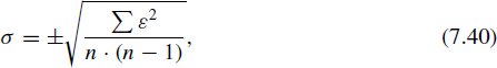
where n is the number of measurements; ε is the deviation of separate measurements from their arithmetical average;
Finally, the results of measurements can be written as

The experimental research of the correlation dependence for the temperature uncertainty of measures was carried out by the simultaneous measurement of frequency on the output fALE/3 of the external divider and the time interval T0 on the output P0.1. The temperature of the quartz-crystal oscillator varied from +18 °C up to +100 °C with consequent cooling. The research of the correlation dependence was carried out by the change of the supply voltage Vdd in the range from +4.7 up to +5.25 V.
Experimental results for errors of frequency and time references are shown in Figure 7.11 and 7.12 respectively. Frequency changes of an output signal of the quartz oscillator during the time interval from 1 ms up to 10 s are stipulated by the thermal noise of a quartz oscillator and elements of the circuit as well as by fluctuations of other parameters. For a short average time, the main destabilizing factor is the thermal noise of the quartz oscillator. Histograms of their distributions are shown in Figures 7.13 and 7.14. The check of distribution laws according to the χ2 criterion has shown that distribution laws of errors of measures are close to the Gaussian distribution law.
Although the frequency and time references are realized with the help of the same internal system clock generator of the microcontroller, the temperature uncertainty of the frequency reference is higher. It is stipulated that the required reference frequency f0 is formed by two internal and one external frequency dividers, introducing contributions to the resulting error of the frequency measure.
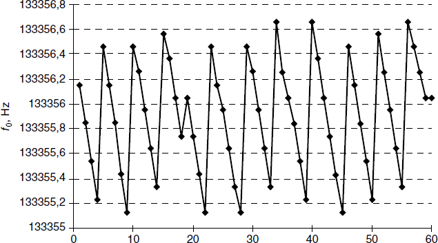
Figure 7.11 Frequency reference error at t = 20°C

Figure 7.12 Time reference error at t = 20°C
The thermal instability of the frequency for the quartz-crystal generator is Δf/f = 11.5 × 10⁻⁶. Dimensions of the measurement accuracy are shown in Table 7.6.
The experimental researches of the temperature uncertainty for frequency and time references realized on the basis of the built-in microcontroller's quartz-crystal generator determined the extreme accuracy of the ‘measurement standard’, which cannot be exceeded for the given technical implementation independently on the method of measurement (conversion) used. The maximum temperature uncertainty of the frequency reference is ±11.5 × 10⁻⁶, and the maximum temperature uncertainty of the time reference is ±0.38 × 10⁻⁶.
Figure 7.13 Histograms of distributions for frequency reference error
Figure 7.14 Histograms of distributions for time reference error
Table 7.6 Dimensions of measurement accuracy at P = 97%

Two components of the reference error considered above are caused by the same reason (frequency instability of the built-in quartz generator) and, hence, are strongly correlated. By the summation of these components, it is necessary to take into account the correlation factor ρ, reflecting that errors of time and frequency references are rigidly and negatively correlated. Generally, it is expedient to present all components by mean-square deviations in order to eliminate the influence of distribution laws from deformation at the error summation:
then the sum of correlated errors is determined according to the formula
If both summable error components are distributed according to the uniform distribution law, the resulting distribution will be trapezoidal. As these errors in these experimental investigations are rigidly and negatively correlated, to find the total error of the measure they should be added algebraically with allowance for the correlation factor ρ. Then the total error of the ‘measurement standard’ in the microcontroller is equal to ±10.9 × 10⁻⁶. As a result of experiments, the rigid inverse correlation of errors for frequency and time references with the correlation factor ρ = −0.981 ± 1.291 × 10⁻⁶ was determined. Correlation dependencies of reference are shown in Figure 7.15.
Further improvement of stability for the built-in quartz-crystal generator of the embedded microcontroller can be achieved by the use of the oven-controlled crystal oscillator. The temperature stability of frequency can also be increased by the frequency control of quartz generators, as realized in the microcontroller of the MSP430 (Texas Instruments) family [129]. Therefore, if necessary, the temperature behaviour of the crystal can also be taken into account. There is the typical dependence of a crystal in relation to its temperature [129]. The nominal frequency is preset at one temperature t0 (turning point); above and below this temperature the frequency is always lower (a negative temperature coefficient). Beside the turning point, the frequency deviation increases with the square of the temperature deviation (−0.035 ppm/°C2 for example). The quadratic equation that describes this temperature behaviour is approximately (t0 = +19 °C):
where Δf is the frequency deviation in ppm; t is the crystal temperature in °C.
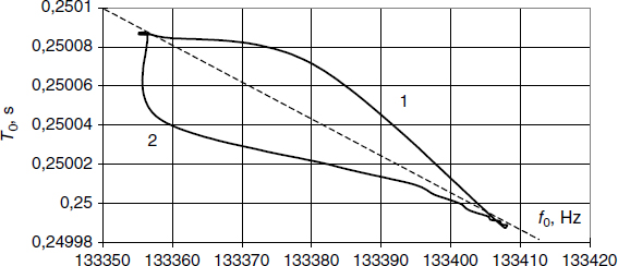
Figure 7.15 Correlation dependencies of reference at heating (2) and cooling (1)
Using the above equation the crystal temperature is measured and the frequency deviation computed every hour. These deviations are added until an accumulated deviation of one second is reached: the counter for seconds is then incremented by one and one second is subtracted from the accumulated deviation, leaving the remainder in the accumulation register.
7.4.2 Calculation error
Inclusion of the processor into a converter measuring circuit and numerical measuring transformations into a measuring procedure changes the structure of the total error. Components caused by numerical measuring transformations appear and the necessity of metrological analysis in connection with conversion algorithm complication arises. It is particularly valid for smart sensors, in which short number bit (8-, 16-bit) microcontrollers are used. On the other hand, there is no necessity essentially to overestimate the requirement for the calculation accuracy in comparison with those errors, which are introduced by other components. It is necessary to assume that the calculation errors could be neglected.
The class of typical computing procedures includes the multiplication and division of multibyte numbers (8-, 16-, 32-, 64-bits) as well as the binary-to-binary-coded decimal code conversion and conversely. Generally, by the PCM realization based on the ratiometric counting method, the calculation of converted frequencies or periods are made according to Equations (5.4) and (5.11) respectively. In general, the limited word capacity of the microcontroller results in two kinds of errors: the numeration error and rounding error. If for the numeration Xn0 bits are used, the numeration error of X is equal to half of the weight of the lowest-order digit and can be determined as
where k is the base of the system of numeration.
The truncation error arises as a result of the word-length reduction after multiplication, division as well as the algebraic summation in view of scaling variables. The same error exists by the operand right shifts.
It is necessary to differentiate between the simple truncation (rejection) and the rounding truncation. The accuracy of the first operation is much lower because the mean is not equal to zero, however its realization is much easier. These components of the error calculation, its characteristics and calculation technique have been described in many references. However, the general theory needs an additional specification with reference to PCM realizations.
In order to increase the computing speed and reduce dynamic errors, the operands realizing dependences (Equations (5.4) and (5.11)) should be used in a fixed point form. Numeration ranges for N1, N2 are determined by the range of converted frequencies [fx min, … fx max]:
Thus, the non-redundant bit number n0, used for the presentation of a number, is achieved. Multibyte operands are stored in packed format in the microcontroller's memory.
Arithmetic subroutines operate with binary, integer, signless operands. The word length of operands should result from the minimum condition of the error arising owing to the word-length limitation. So, for multiplication, it is expedient to use the multiplication method by the low-order digit ahead with the shift to the right of the partial product. This method works according to the exact multiplication scheme. For multibyte division, it is expedient to use the division method with the shift to the left and the residue restoration. Moreover, by the execution of the division subroutine, it is necessary to check if the denominator equals zero and to process the ‘divide by zero’ error. The secondary effect of these actions is an opportunity to determine the failure in the reference frequency channel. So, the equality N2 = 0 testifies about the problem with the pulse propagation in the frequency divider → timer/counter's input path.
Because the microcontroller's data memory, whose size determines the possible length of operands and results, is used for operands and results storage the accuracy of arithmetic operations is not limited by the word length of the microcontroller, and δcalc ![]() δq.
δq.
Generally, in Equation (5.4), the reference frequency f0 is constant and does not belong to the set of integers Z. Then, with the aim of using the integer arithmetic to increase the computing operation accuracy, it is expedient to use scaling by the multiplication of the numerator and the denominator to scale the factor km. The use of the multiplication according to the exact scheme with the required word length by which the multiplication result of three nx−, ny− and nz− bit numbers has nx + ny + nz bits, and the certain execution order for mathematical operations with the same priority (three multiplications, then the division), minimizes the calculation error. Thus, the truncation error appears, only at the last stage of calculations which is determined by the number of bits necessary for the representation of the remainder of division.
In view of scaling, the final calculations of frequency should be made according to the formula
As f0 · km = K = const, the final equation will be:
In order to reduce the resulting calculation error, it is necessary to accept the following execution order for arithmetic operations of the same priority:
The final number of bits for operands and results representation are determined by the range of converted frequencies fx ∈ [fx min, fx max], the range of numbers N1, N2 (Equations (7.48), (7.49) respectively), scaling and requirements of universality of arithmetic subroutines.
7.4.3 Error of T02 forming
The PCM analysis has revealed a number of additional components of the conversion error, connected with the forming of second reference time interval T02. The error of forming the T02 includes two components: the error of the wavefront and the wavetail forming (Figure 7.16). In its turn, the last component includes the error due to the delay of reaction to interruption, and the error of the shift in time of the response for interruption.
The delay of the reaction to interruption (the time interval between the pulse of the frequency fx on the interrupt input and the timer/counter start) is determined by the execution time for three instructions: (1) CALL to the interrupt vector; (2) the unconditional jump (JMP) to the interruption subroutine; (3) the start timer/counter:
The delay Δτdelay ≥ 1/f0 is the reason for the systematic error because of the T02 reduction connected with the execution time of three commands mentioned above.
In its turn, the shift in time of the response for interruption also brings an additional component into the resulting conversion error distributed according to the uniform law of the distribution. The reason for this component is that the time used by the microcontroller for the response to interruption can vary. So, microcontrollers of MCS-51/52/196 families (Intel) answer to the interruption as a rule at the end of the current instruction cycle as well as for the majority of other microcontrollers. As the maximum instruction cycle, during which interruptions from fx are possible (the program for forming the gate time T01) is
where τcycle is the machine cycle duration, and can vary, for example, in time reduction, so that the necessary time for the response to interruption is changed in limits Δτ′delay ∈]0; τc max].
The error of the T02 wavetail forming is determined by the delay Δτ″, connected with the execution of the instruction of the logic polling for the last pulse of the frequency fx. Its value is in the interval Δτ″ ∈ [3τcycle, 5τcycle] and is determined by the logic of the execution of the program part of the last pulse fx polling. Then the real value of the gate time T02 is determined as

Figure 7.16 Reasons for instrumental error
The influence of the error of shift in time of the response for interruption and errors because of the T02 wavetail forming can be mutually compensated as the first component reduces the gate time T02 and the second increases it. The reduction of the error of shift in time of the response for the interruption can be achieved using a higher-speed microcontroller core or increased microcontroller clock frequency. In its turn, such measures will also result in the quantization error reduction as the frequency f0 value in Equation (5.7) also will be increased.
7.5 Correction of PCM's Systematic Errors
The inclusion of the embedded microcontroller or the microcontroller core into smart sensors provides opportunities for the use of known methods of automatic error correction for measurement results, improvements to existing of methods and the creation of new methods.
The increase of the accuracy of frequency-to-code converters is possible due to the conversion algorithm improvement as well as to the use of additional data processing and calculation in order to correct conversion results. The first group of methods is focused on the reduction of methodical errors, the second group reduces both methodical and instrumentation errors. Thus PCM error reduction is possible at high conversion speed and without the essential algorithmic complication.
A number of additional error components revealed by PCM analysis can be reduced by systematic error elimination by a design stage of the PCM software.
As one of the main metrological features of frequency-to-code converters based on a PCM is the dependence of the conversion result on the PCM algorithmic structure and the software realization, then such methods increasing the conversion accuracy can be extended due to algorithmic methods of errors reduction alongside constructive-technological and protective-safety methods. The method, used for reduction of the gate time T01 forming error, because of the delay of reaction to interruption (Equation (7.52)) is one elementary way for the aprioristic elimination of systematic errors. The essence of this method consists of the change of the rigidly established instruction order for interrupts subroutine from external sources (converted frequencies fx) by the service protocol for external interruptions. For the Δτdelay reduction, the interruptions subroutine is modified so that whenever possible the instruction to the start timer/counter is executed as soon as possible.
For this aim, instead of the unconditional jump instruction, the start timer/counter instruction is placed in the memory cell of the external interrupt vector as specified by the service protocol of external interruptions. In its turn, the unconditional jump instruction JMP for the interruptions subroutine from pulses fx is located in the next memory cell. Then Δτdelay is determined by the execution time for only two instructions instead of three and is equal to
instead of 5τcycle.
As the systematic error Δτdelay residue is no eliminated at this stage, and is still commensurable with the period T0 of the reference frequency, it can be finally eliminated at the calculation stage of the converted frequency fx according to Equation (5.4) with the help of the corrective action for N2 by increment of its lowest-order byte.
Addresses of interrupt vectors in microcontroller families MCS-51/52 (Intel) are located in the resident memory with the interval in 8 bytes. Hence, this method of systematic error elimination can be successfully used for frequency-to-code converters based on this microcontroller family.
The instrumentation error Δτ′delay can be reduced by constructive-technological methods because of the shift in time of the response for interruption: that is by using a higher-speed microcontroller or increasing clock frequency if possible.
The real value of the gate time T02 after elimination of the error component Δτdelay will look like
Thus, the method used for the algorithmic aprioristic elimination of systematic errors at in PCM software design reduces the error component Δτdelay of the T02 wavefront forming practically without algorithmic and software complication. In its turn, further correction at the minimum algorithmic PCM complication (one additional one-byte instruction, INC 〈register〉) eliminates the time delay Δτdelay completely.
As in this case, the condition for correction usage is determined by the inequality
where Δtcorrection is the corrected time interval, the correction at the initial stage would not give an opportunity for full elimination of the error Δτdelay because of the non-valid condition (Equation (7.57)). The combination of this method for aprioristic elimination of the error reasons and corrective action in the final result of the determination N1 gives the effect of full elimination of Δτdelay. Thus, main systematic conversion errors can be eliminated by software design.
7.6 Modified Method of Algorithm Merging for PCMs
In designing multifunctional frequency (phase shift)-to-code converters for smart sensors based on modern microcontrollers, there is a problem of the resident memory economy, and consequently, the chip area. The task of memory size minimization for the PCM software consists of using methods of algorithm merging for union into a combined algorithms, reflecting the specificity of the solution in special situations. The precondition for this is a coincidence of some basic operations of elementary measuring procedures of PCM algorithms. However, existing methods of algorithm merging offered by Karp, Lazarev and Piyl’ [141] as well as modification of Karp's algorithm [142], using partial matrix algorithm schemes, do not take into account, that during each combined algorithm execution, interruptions and the subroutine execution according to the required algorithms of functioning are possible. In the combined algorithm, it is also necessary to provide an opportunity of work with appropriate internal (from timer/counters) and external (hardware) interruptions at a limited number of interrupt vectors. Therefore, the method using partial matrix algorithm schemes was modified [143]. Thus, the modified method consists of the following:
- According to initial block diagrams of two algorithms A and B, having common operators, partial matrixes
 and
and  , reflecting relationships of common operators are constructed. Their elements are represented by the Boolean function determining conditions of transition from the operator i to the operator j. The binary variable Σ is used for the indication of what should be realized from two variants of the combined algorithm. Let the value Σ = 1 correspond to the algorithm A, and the value
  = 1 to the algorithm B. The practical realization of the Boolean variable Σ is carried out simply enough by the set up or reset of the use bit.
 - Additional rows, Nij, are included in partial matrixes of algorithms and . Their elements are represented by Boolean variables determining the conditions of interrupts subroutines calls during the execution of appropriate operators of algorithms and reflecting relationships of common interruptions subroutines. If the interruption during the execution of the ith operator is enabled, the Boolean variable in this row is equal to ‘1’, otherwise to ‘0’. Dimensions of partial matrixes of algorithms A and B are equal to ((q + Nij)NA) × ((q + Nij)NB) accordingly, where q is the number of common operators; NA and NB are the number of all operators in algorithms A and B respectively.
- In view of the additional row the partial matrix
 of the combined algorithm with dimension (q + Nij) × (NA + NB − q) is constructed
- The partial matrix at the third stage is simplified whenever possible by extraction of the disjunctive equation
Let's pass from the final partial matrix to the partial block diagram of the combined algorithm. Further, accepting that step by step Σ = 1 and ![]() = 1 and adding to the block diagram the rest parts of the block diagrams of algorithms A and B and we obtain the full block diagram of the combined algorithm. It is supplemented by conditional operators, whose dependence on the variable Σ enables or disables interruptions subroutines by the execution of this or that operator of the merged algorithm and modifies virtual interrupt vectors, thus providing the initialization of the required subroutine.
= 1 and adding to the block diagram the rest parts of the block diagrams of algorithms A and B and we obtain the full block diagram of the combined algorithm. It is supplemented by conditional operators, whose dependence on the variable Σ enables or disables interruptions subroutines by the execution of this or that operator of the merged algorithm and modifies virtual interrupt vectors, thus providing the initialization of the required subroutine.
If united algorithms use different interruptions subroutines of a large size, it is expedient to merge algorithms of these subroutines with the help of Karp's modified method [142].
From the point of view of the theory of sets, the algorithms merging for PCMs of the frequency and the phase shift can be represented as the union of two sets, one of which is represented by the intersection of sets of operators of algorithms A and B, and the second by its symmetric difference:
where AB = {x : x ∈ A and ![]() ∈ B}, BA = {x : x ∈ B
∈ B}, BA = {x : x ∈ B ![]() ∈ A}.
∈ A}.
Now is a good time to give a practical example. Let algorithm A be the algorithm of the optimum PCM, realizing the frequency-to-code conversion according to the ratiometric counting method. In its turn, algorithm B is the PCM algorithm for the phase shift-to-code conversion. The conversion method for the phase shift based on the determination of the average value tx and the average value of the period Tx during the cycle Tcycle
is used as the PCM basis. Hence, the conversion time is fixed in the certain interval and multiplied by the period Tx. Due to this, the errors of the aliquant of Tcycle and the period Tx are eliminated. The frequency conversion range is extended down to infralow frequencies. Time diagrams of this method are shown in Figure 7.17.
Thus, there are the following features of using functional-logic possibilities of the microcontroller. The pulse counting of the reference frequency f0 is carried out by the timer/counter. Pulses 1, 2 formed by the input shaper, come on the interrupt input INT. The reference time interval nT0 is formed with the help of the program delay, and the interval Tcycle by means of logic analysis. Upon ending of the conversion cycle, we receive two numbers

Figure 7.17 Time diagrams of phase-shift-to-code conversion method
and
The microcontroller calculates the average value of the phase shift according to the following equation:
The coincidence of basic elementary measuring procedures of algorithms A and B allows algorithm merging. Block diagrams of conversion algorithms for the frequency and phase shift are shown in Figure 7.18(a) and (b) respectively. Common operators are shown by identical symbols. Here q = 7, nA = 9 and nB = 9.
After execution of the first two stages of the algorithm merging, we obtain the following partial matrices:

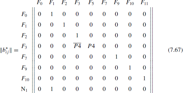

Figure 7.18 Block diagrams for frequency (a) and phase shift (b) to code conversion algorithms
The partial matrix of the combined algorithm is the result of the next stage:

After replacement of ![]() and
and ![]() it is possible to construct the partial block diagram shown in Figure by 7.19 by solid lines. The addition to the full block diagram of the combined algorithm is shown by the dashed line.
it is possible to construct the partial block diagram shown in Figure by 7.19 by solid lines. The addition to the full block diagram of the combined algorithm is shown by the dashed line.
To move on from block diagrams of algorithms to their compact representation by the logic scheme of algorithms, we obtain for algorithm A (frequency conversion)
for algorithm B (phase shift conversion)
and for the combined algorithm of the multifunctional converter

where Fi is the processing operator; Pj is the conditional operator (conditional jump); w is the unconditional jump operator; (END) is the end operator of the logic scheme of the algorithm. This modified method of algorithm merging for PCMs has all the advantages of the modified Karp's method (the reduction of a number of operations at all stages due to the manipulation of smaller dimension matrixes), and also eliminates the inexactness inherent to Karp's method when a common operator in one algorithm is the last one, and in the other algorithm it is not. It also provides algorithmic functioning in conditions of possible interruptions. This method of algorithm merging reduces the resident memory size of the microcontroller by the realization of the multifunction converter for frequency-time parameters by two times.
Modified methods of algorithm merging based on partial matrix schemes of algorithms solves the problem of minimization for embedded memory in the smart sensor microcontroller or the microcontroller core only partially. By the synthesis of processor algorithms of the PCM there is the accompanying task of memory size minimization for the realization of algorithms composed from separate parts. With the aim to reduce the memory size, common parts can be allocated as subroutines S1, S2, …, Sλ.
Let Vj be the memory size, occupied by the jth common part. For the subroutine initialization and return from it, it is necessary to execute two instructions: ACALL (or LCALL) and RET. The memory size, occupied by the control instruction, is given by
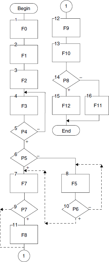
Figure 7.19 Block diagram for combined algorithm
where VjCALL is the part Vlj, related to each of programs using Sj (the call instruction for the subroutine CALL), and VjRET is the part Vlj that belongs only to the subroutine Sj (the return instruction from the subroutine RET).
For real memory saving by subroutine allocation, the minimum number nj of subroutine calls Sj from any programs from a higher level of hierarchy, is calculated as
From here
If the jth part code of size Vj is common for the programs, the number of which is less than nj, there will not be a gain in memory from the allocation in a subroutine and it is expedient to include their operators directly in the program body.
Summary
The use of PCMs for frequency-to-code conversion in digital output smart sensors with embedded microcontrollers reduces hardware, increases reliability, lowers the time-to-market period by the sensor design due to the reusing of software components and realizes sensors' self-adaptive capabilities (software-controlled performances and functional capabilities) in full.
In its turn, the method of algorithm merging reduces the memory size of the embedded microcontroller, which also contributes to hardware reduction.