
8
Digital Signal Processors
8.1 DIGITAL SIGNAL PROCESSING
To illustrate how to design and implement application-specific processing systems we consider a special application domain, the processing of continuous (‘analog’) signals. The importance of this area is obvious from the fact that the signals occurring in physical systems are primarily of this kind. Classically, such signals have been processed through electronic components such as networks of resistors, capacitors, operational amplifiers and non-linear circuits, implementing filters, modulators, and computational operations. Complex processing functions realized with such means suffer from the lack of reproducibility, precision, dependency on temperature, noise, etc. which are not present in digital processors (at the expense of much higher circuit complexities).
8.1.1 Analog-to-Digital Conversion
The first step to be taken to process a continuous input, e.g. a time-varying voltage e(t) ranging in some interval [U1, U2], by means of a digital processor is to perform a conversion of the input value at a given time t0 into an encoded number (the A/D conversion). e(t0) is called a sample of the time function e taken at t0. Reciprocally, the digital processor outputs encoded numbers that have to be converted into a continuous signal with a proportional magnitude (the D/A conversion).
The most basic step towards performing such a conversion is the comparator that compares the input voltage e to a reference voltage r. The output is H if e > r + d and L if e < r − d for some small value d, and unspecified otherwise. The comparator is realized as a high gain difference amplifier that is driven to saturation once the absolute input difference is above d. To avoid a constant input near r producing an oscillating output due to the presence of noise, the comparator may be given a hysteresis. As usual, such a circuit needs a processing time from applying the input to getting the valid output (10 ns..10 μs, depending on the circuit and on d). In order to perform the comparison at the specific time to, it may be necessary to ‘freeze’ the input to the comparator during this processing time in a sample and hold circuit and then freeze the output in a storage circuit until it is actually read by the digital processor. The input hold circuit may be realized by a capacitor at the input to the comparator that is disconnected from the input source at the time t0.
In order to perform the conversion of an input voltage e ranging in [0, U] w.r.t. some reference potential into an n-bit binary code representing the integer m < 2n so that 0V ≤ e − mU/2n < U/2n, a number of comparison operations are carried out in parallel or serially (keeping the analogue input frozen as long as necessary). A parallel conversion would use 2n−1 comparators with the references connected to the values mU/2n. The 2n−1 output bits of the comparators would be digitally encoded in the desired n-bit word. The reference voltages can be derived from a single reference r = U by means of a ladder of 2n resistors connected in series. Such circuits are the fastest A/D converters and are called flash converters. They are available as integrated circuits for n ≤ 10 with conversion rates of up to several 100 MHz.
For a serial conversion, a single comparator can be used by applying a series of reference voltages. Not all reference values of the parallel conversion are needed. Instead, the first comparison is with the ½ U reference; then it is known in which of the intervals [0, U/2] or [U/2, U] the input is located and the search for the right code is continued there. One actually performs a binary search for the best fitting code, using n comparisons only. This method is called successive approximation. Converters based on it are also available as integrated circuits for n ≤ 16 and conversion rates of up to several MHz. There are also intermediate converters performing some comparisons in parallel, and high-speed converters suitable for digitizing video signals that perform subsequent comparisons of the successive approximation in a pipeline using several comparators. They operate at the through-put rates of flash converters, but need a higher processing time, and n comparators only. The highest resolution converters, used e.g. for digital volt meters, apply all reference values in a linear fashion, actually a continuous linear ramp and perform the equivalent of a time measurement.
The conversion locates the input voltage in one of 2n intervals of size U/2n. W.r.t. the centers of these intervals the actual input differs by a maximum of U/2n+1, the so-called quantization error. There are additional errors due to the generation of the reference voltages and also to the gains and offsets of the comparators.
The basic element of the D/A conversion is the electronic switch controlled by a digital output, simply an n-channel transistor in saturation that behaves like a resistor with a very low resistance if H is applied to its gate, and a very high resistance if L is applied. If the switch is used to connect a resistor R driven by a reference voltage U to a summing node, a current of I = U/R or 0 depending on the digital input enters the node. The logic output is not used to directly drive the resistor as the H and L intervals are intentionally large and would not allow a precise output. The current can be converted to a voltage by means of an operational amplifier if needed [19]. An n-bit binary number can be converted into a proportional current by letting each bit switch a current to the summing node and letting the ith bit control the current Ii = 2iI0 = U/(R/2i). The set n weighted currents Ii is easily obtained from a so-called R–2R network of resistors of the same size which is easier to manufacture (Figure 8.1). Such resistor networks along with the switches are available as integrated circuits for n ≤ 16. This type of D/A converter has the additional property that the analogue output is strictly proportional to the reference U. It may e.g. be used to implement a digital gain control into an amplifier circuit.

Figure 8.1 D/A converter using an R/2R ladder
Another way to convert a multi-bit word is to generate a pulse width modulated signal (PWM) by connecting a digital n-bit comparator to the output of a free running n-bit counter. If the PWM output controls the switch, the average current is proportional to the pulse width and hence to the input of the comparator. The period of the signal is given by the counter clock period times 2n; typically for this method, n ≤ 12. The period must be adjusted to the averaging performed on the pulses by means of some analog filter. More generally, a signal may be represented as a continuous sequence of single-bit numbers clocked out at a high rate and passed through a converter that changes the bit values into voltages or currents. These are integrated by an analog filter to yield a smooth analog signal output. This method is e.g. used for audio converters and ‘digital’ power amplifiers.
8.1.2 Signal Sampling
If a digital processor is used to process a time varying signal, the signal is converted into a series of samples taken periodically with a sampling frequency fs (taking equispaced samples is the usual way). Thus the continuous time signal e(t) is converted into the series of numbers en = e(t0+n/fs). The well-known sampling theorem states that the continuous time signal can be recovered from the series en of equispaced samples if fs is chosen to be larger than twice the bandwidth b of the signal (i.e. in the representation of the real signal as a superposition of phase-shifted sin(ωt) signals obtained through the Fourier transform, no components with a higher frequency than b occur). Thus no information about the signal is lost by just considering the chosen samples, and all processing of the original signal can – in principle – be substituted by a processing of the samples. If the processing results in another signal g(t) of at most the same bandwidth, then it suffices to calculate samples gn of it at a rate given by the same frequency fs. The signal g(t) can then be reconstructed from the gn according to the following formula. If its bandwidth is lower, a lower rate ![]() suffices.
suffices.
![]()
The A/D conversion can e.g. be simplified by sampling the signal at a much higher rate than required by the sampling theorem using a single-bit converter (a comparator) only and some analog preprocessing. The resulting bit sequence (bn) is passed through a digital filtering processor that computes high resolution samples, the rate of which is reduced according to the bandwidth. The Σ-Δ-converter structure shown in Figure 8.2 is e.g. used for audio signals [14]. It requires continuous operation (in contrast to taking individual samples) and some processing delay for the digital filtering. Such converters are offered as integrated standard components by several manufacturers.

Figure 8.2 Σ-Δ-conversion

Figure 8.3 Complex sampling and baseband sampling
The sampling theorem and the reconstruction formula hold for ‘baseband’ signals having Fourier components in the interval [−b, b] only. With a simple modification, it carries over to the case of a narrow-band signal centered around some carrier frequency f0. A signal of this kind can be represented as:
![]()
The pair of signals (er(t), ei(t)) is the complex amplitude modulating the carrier. It only has frequency components in [−b/2, b/2] and needs to be sampled with a frequency of at least b (in total, real samples are needed with a minimum rate of 2b). An easy way to obtain samples of (er(t), ei(t)) without having to generate and premultiply the cos(ωt) and sin(ωt) signals (with a small superimposed error that increases with the bandwidth) is to choose the sampling frequency to be fs = 4f0. If g, h are subsequent samples of e(t), then 2−½(h + g, h − g) can be used as samples of (er(t), ei(t)) at the midpoint between the sampling times for g and h and taken at a reduced rate due to the assumed low bandwidth. This procedure called complex (or ‘quadrature’) sampling amounts to taking pairs of samples separated by about a quarter of the carrier period at a reduced rate (Figure 8.3). It corresponds to continuously sampling the signal with the rate of fs, multiplying by the samples of the complex carrier, filtering by summing up adjacent samples to suppress signal components near fs/2, and then sub-sampling according to the bandwidth. The operation of forming (h + g, h − g) can be combined with the further processing of the samples. The approximation error for the complex samples can be further reduced by using more than two subsequent samples for each, e.g. by replacing the sum ½(h + g) by its mean value with an extra sample taken at the mid-point.
Instead of processing a single time signal e(t), a DSP system may be used to process an array of signals so that the samples become complex, indexed data structures. As well as depending on the time variable the signal may depend on other, continuous input variables as well. An example of this kind is the intensity e(x, y, t) of the light emitted from an image. All coordinates would be sampled so that the signal is converted into an array of ‘pixels’ ei, j,n, with 0 ≤ i ≤ Nx, 0 ≤ j ≤ Ny and n being the time index. For a colored video signal, there would be additional signals defining the color, or separate intensities eR, eG, eB would be used for the red, green and blue components. For video signals the time parameter is usually sampled at image rates of up to a few 100 Hz only, but for typical spatial resolutions of Nx, Ny = 300..1600, every image sample may contain a million pixels that need to be processed, input and output at the image rates. One to two subsequent images are usually stored in 2D storage arrays providing indexed access to the pixels.
Figure 8.4 Analog video signal
Video signals are transmitted using a single analog signal to sequentially transfer images line by line within the image sample interval synchronously to the electron beam scanning the screen of a display tube, and suitable to directly modulate its intensity. For an analog video signal, the x coordinate is continuous, but the y and t coordinates are replaced by the discrete coordinates j, n. Synchronizing events identifying the start of a new image sample and within an image the start of every new line are transferred separately or integrated into the video signal as well forming a ‘composite’ video signal with a precisely defined timing (Figure 8.4). There are special A/D converter chips such as the SAA7113 from Philips that convert an analog video signal as it would e.g. be generated by a CCD image sensor chip into a serial data stream of digital words transmitted along with separate clock and frame synchronization signals. CCD imaging chips are an integrated array of photoelectric sensors. The charge coupled device (CCD) technology is used to shift out the analog signals (charges) generated at the individual sensor pixels and to output them in a time serial fashion through a synthetic video signal. Charge can be transferred from a capacitor to a neighboring one in a chain by raising its foot-point potential and discharging it to the other one down to a threshold through a transistor switch (with a loss of energy, other than in Figure 2.25). For the generation of video signals, fast D/A converters convert triple input words into the analog signals required for the red, green, and blue (RGB) pixel intensities of a cathode ray display tube (CRT) or a TFT monitor with a compatible interface.
8.1.3 DSP System Structure
The set-up of a digital signal processing system transforming a band limited signal e(t) into another signal g(t) is as shown in Figure 8.5. The signal is converted into a sequence of samples en taken at the sampling rate fs. If the signal contains components outside the band to be processed, a low pass filter must be used to definitely limit the band to less than ½fs. Otherwise higher frequency components would show up (alias) in the samples in the same way as base band frequencies. For typical audio signal processors, the en are signed 16-bit numbers using the 2's complement integer encoding. The 16-bit samples gm would be computed by the processor at some rate ![]() as required for the bandwidth of the signal g(t) and output to an D/A converter. The resulting staircase wave-form is then smoothed by another low pass filter to perform the interpolation.
as required for the bandwidth of the signal g(t) and output to an D/A converter. The resulting staircase wave-form is then smoothed by another low pass filter to perform the interpolation.
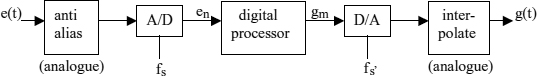
Figure 8.5 DSP system structure with analogue input and output
A large number of filtering operations can be moved to the digital domain in this way. Any frequency response can in fact be arbitrarily approximated by a digital processor. An important consequence of this set-up is that the digital processor operates under the constraint that the time available for the processing of an individual output sample is limited by the output sampling period ![]() . For audio processing e.g., a standard sampling rate both at the input and at the output is 48 kHz which translates into an allowed time per sample output of 21 μs. In order to simplify the analog filters the input sampling rate can be increased. Then the digital processor can perform a low pass filter computation at the smaller sampling rate before further processing the samples. Similarly, the interpolation can be performed partly by the digital processor, so that interpolated samples are output at a higher rate.
. For audio processing e.g., a standard sampling rate both at the input and at the output is 48 kHz which translates into an allowed time per sample output of 21 μs. In order to simplify the analog filters the input sampling rate can be increased. Then the digital processor can perform a low pass filter computation at the smaller sampling rate before further processing the samples. Similarly, the interpolation can be performed partly by the digital processor, so that interpolated samples are output at a higher rate.
Applications other than filtering can just input some signals but not generate a continuous output signal but perform some other processing to e.g. detect patterns in the signal for such purposes as speech or object recognition and localization, or to perform some signal analysis and display the results. Also, there are many applications in which a DSP does not input signal samples at all but synthesizes and outputs complex signals (e.g., audio or video signals). A periodic audio signal can e.g. be synthesized by storing a set of samples representing a single period (a ‘wave table’). A set of 256 samples would e.g. cover more than 100 overtones. The wave table can be read out periodically at the audio sampling rate and be output to the D/A converters. If a different frequency is required, it is read out by stepping through it at a different pace, interpolating between adjacent samples if required.
For the special case of video signals, a processor may be used to perform pattern recognition in images captured from a video sensor, or to synthesize and output complex images sequences. A low resolution monochrome CCD sensor as e.g. used in simple robotics applications would deliver 384 × 288 × 25 pixels per second. For video output, a rate considered low-end would be 640 × 480 × 50, each pixel being encoded by separate 8-bit numbers for the R, G and B components (in total 24 bits per pixel). Even if there is no change to the image data, the output to a display would require the continuous generation of an output data stream of 15M bytes/s from an image ‘frame’ buffer memory of nearly 1 M bytes. The synthesis and the processing of video signals require very high processing rates supported by dedicated hardware, fast interfaces and large memory buffers.
Compression and decompression of the video data are essential for communicating and storing image data [75], but also for the synthesis of visual output. The 24 bits per pixel may e.g. be reduced to 8 bits by using a table of 256 entries to associate 24-bit RGB values to 8-bit codes. The combination of such a table with the D/A converters for the RGB outputs is a common component of video signal generators called a color palette. The outputting is still at a rate of 5M bytes/s from a frame buffer of 300 k bytes. The simplest form of hardware-supported decompression is the use of character generators for textual output to a video display. Characters are displayed as sub-images of, say, 8 × 16 single-bit (black or white) pixels that are selected by the display circuit from a ROM table using the 8-bit ASCII character code as a table index. Then only a page of a 2400 character codes remains to be output from a memory buffer to the video processing circuit at the rate of 50 Hz (120 k bytes/s) to generate a 640 × 480 monochrome video signal using some DMA circuit.

Figure 8.6 Triangle painting
Graphical displays do not use this kind of on-the-fly decompression but output pixel-by-pixel from a large frame buffer at a high rate. Synthetic images are decompressed from a much smaller data structure and written into the frame buffer in a number of steps (the so-called rendering pipeline [74]) that can be supported through hardware circuits to generate the pixel data at the required rate. The image is usually represented as a set of triangle coordinates, some of which have to be displayed and filled with various patterns using special, fast algorithms. The endpoints of the fill lines can be interpolated from the triangle coordinates by performing incremental add and compare operations only, and the same applies to interpolating the pixel values or to copying them from some texture template (Figure 8.6). A triangle is filled line by line to exploit the fast page mode access to a video RAM addressed so that lines are contained within pages. The overwriting of pixels in the foreground can be inhibited by storing a z-coordinate for each pixel (in a ‘z-buffer’) or by ordering and selecting the triangles to be displayed. Changing views and the motion of objects in a 3D scene are realized by performing affine coordinate transformations on the triangles. Recent dedicated graphics chips perform this synthesis of video data into a fast video frame memory by employing a considerable amount of hardware, exploiting the possibility to compute several pixels in parallel. The multi-media operations found in the workstation class processors or an SH-4 (6.6.4) also support the synthesis of video data.
Synthetic video (and audio) signals are thus expanded from fairly small parameter sets to implement the man–machine interface (and thereby become enriched by secondary effects at the ‘man’ side). Temporal filtering of the sequence images is used for data compression (by encoding changes of subsequent images). Filtering is used in the x and y directions only for various image analysis and enhancement steps [67]. Some common image processing steps are non-linear and implemented by special Boolean operations on the pixel values. In the subsequent discussion of DSP algorithms and processors, we concentrate on some basic linear algorithms that apply to time signals e(t) and multi-dimensional signals (e.g., e(x, y, t)) as well.
8.2 DSP ALGORITHMS
In this section, some common DSP algorithms applied to the sequences of samples taken from some signal e(t) are considered. The main reference on this is [14]. [62] is an introduction also covering implementations on a DSP chip, and [3] explains the relationship of algorithms and architectures. An analysis of their complexity and the available time reveals that even for the moderate audio sample rates the computational requirements are significant.
8.2.1 FIR Filters
A standard algorithm for digital filtering is the FIR filter. Here:
The sequence (gn) is the convolution product of the input sequence by the finite sequence of coefficients (cj). The formula defines gn as the dot product of two vectors which is a general linear operation that comes up in many other contexts as well, e.g. as the basic operation in artificial neural networks. The length N of the filter is determined by the resolution with which a desired frequency response may be prescribed. The coefficients can be computed to produce any independently prescribed gains and phase shifts to the sampled sine input sequences of integer multiples by k of the frequency fs/N, for −N/2 < k < N/2. As a rule of thumb, such a filter can implement a narrow band pass of the width 2fs/N. If an audio equalizer has to be built that allows the gain setting for sub bands of width 100 Hz, then for fs = 48 kHz, N is about 1000. Typically, the filter output is computed at the input sampling rate. N determines the amount of processing per sample and number of input samples required and to be stored for the computation. For N = 1000, the time available to process a sample translates into a frequency of 96 million arithmetical operations per second.
The en and ci in equation (1) are real numbers that have to be encoded on a DSP. Samples usually come up in a fixed point format, and the coefficients ranging in the interval (−1, 1) may be encoded in a similar way. The FIR algorithm with a 16-bit integer input and 16-bit fixed point coefficient data performs signed 16 × 16-bit multiplications which have a 31 bit result, of which the upper 16 bits represent a voltage in the input range. If 16 bits are needed for the final result and every product were rounded to 16 places, the rounding error could be as high as 2−16 and accumulate through the summation to N*2−16 in the worst case (in practice, this would not happen). In order to avoid this for arbitrary N, the summation can be implemented to take care of the full product words. If a 16-bit output encoding is needed, a rounding operation from the 14th place is required (the 0th is the least significant bit, LSB). In the summation overflow may occur beyond the 31-bit word size. This can be handled by providing a wider word size for the sum. Implementations use 8 extra bits allowing the improbable event of 256 full size products of the same sign to accumulate (Figure 8.7). If at the end some of the extra bits are unequal to the sign bit of the lower 16 bits of the rounded result word (overflow condition), the result cannot be represented with 16 bits. In this case the 16-bit result is substituted by the most negative or the most positive 16-bit value in order to obtain an overflow behavior similar to that of an amplifier circuit (saturation).
An important special case of the FIR filter is the symmetric FIR filter with the additional property that ci = cN−i−i. These are common as symmetry corresponds to the property of linear phase or constant group delay [14]. For the symmetric FIR filter, the distributive law can be applied to arrive at a simpler algorithm to compute the FIR output gn:
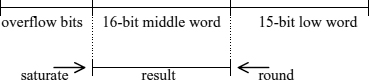
Figure 8.7 Conversion from the result of the fixed point FIR computation
If samples and coefficients are encoded as 16-bit numbers again, the sum of two samples is a 17-bit number, and the multiplication is a signed 16-bit by 17-bit one.
The least mean squares (LMS) algorithm is an extension to the FIR algorithms that adapts the coefficients of the FIR filter in order to let the output become similar to a reference sequence (sn) in the sense that the difference sequence (sn−gn) should have a low energy [61]. The adaptation rule for the coefficients ci after computing gn using (1) is:
where ε is a small constant. If the adaptation step (3) is executed at the sampling rate, another N products and sums need to be computed. The LMS algorithm can also be applied to symmetric filters. Then the adaptation rule for the ci becomes:
![]()
8.2.2 Fast Fourier Transform
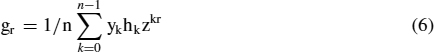
The discrete Fourier transform (DFT) serves to transform a finite real or complex vector of samples (xr), r = 0,..,n − 1 into the frequency domain, i.e. to represent it as a linear superposition of complex sine vectors. The complex sine vector with the normalized frequency k that circles k times around the unit circle if r runs from 0 to n − 1 is the sequence (zkr), with z = e2πi/n. This can in turn be used to implement filters that multiply this sine sequence considered as a periodic sequence of signal samples by a constant complex phase factor hk. For 0 ≤ k < n the kth Fourier coefficient of the sequence x is the dot product:

With these coefficients, x can be expressed as:

and the filter applied to the (cyclically repeated) sequence (xr) yields the (periodic) output sequence:
The DFT transforming the sequence (xr) into the sequence (yk) consumes O(n2) operations but can be simplified to the fast Fourier transform (FFT). If n is even, using the identity zn/2 = − 1 we obtain for 0 ≤ k < n/2:


Thus the DFT breaks up into two half size DFTs applied to the sequences (e2r) and (e2r+1) followed by n/2 operations of the type:
the so-called FFT butterflies (cf. Chapter 1, exercise 7). If n is a power of 2, n = 2m, the same procedure can be continued with the half size DFTs, obtaining 4 quarter size DFTs etc., and the DFT is performed in m ‘passes’ of n/2 butterflies. The final pass uses the factors w = z−k, k < n/2, the one before twice the w = (z2)−k, k < n/4, the first pass does not use multiplication at all, and the second uses w = −i only, which is a formal operation not needing a multiplier. Thus the first two passes do not really contribute multiply operations. Each butterfly comprises 2 complex adds and a complex multiply (6 real adds and 4 real multiplies), and has 4 real input and 4 real outputs. This is the radix-2 decimation in time FFT algorithm which hence contains n/2* log2n butterflies and reduces the complexity from O(n2) to O(n logn). The FFT is the result of the ‘divide and conquer’ principle applied to the DFT.
In a similar fashion, the Fourier coefficients yk, yk+n/4, yk+n/2, yk+3N/4 can be rewritten for 0 ≤ k < n/4 using the identity zn/4 = i, to perform the DFT for n = 4m in n/4* m operations of the type:
called radix-4 butterflies and comprising 8 complex adds (4 of the 12 adds in equation (9) can be shared) and 3 complex multiplies (22 real adds and 8 real multiplies) as the multiplication by i is just formal, and 8 real inputs and 8 real outputs. The first pass actually does not contribute real multiplies at all. Compared to the radix-2 transform, the number of multiplies is further reduced by 25%.
If the input x to the DFT is real, the Fourier coefficients yk fulfill the symmetry relation:
with ‘°’ denoting complex conjugation. Thus, both yk and yn−1−k do not need to be computed. Further to just simplify the final butterfly pass, the computation of the FFT can actually be reduced to a half size FFT. Let x′ and x″ denote the vectors (x2r) and (x2r+1), 0 ≤ r < n/2, and xc = x′ + i x″. If y′, y″ and yc are corresponding Fourier transforms, then yc = y′ + i y″. According to equation (10), y′ and y″ can be obtained from yc as:
From equations (7a) and (7b) we conclude:
Thus for n = 2m, the effort to compute y via the FFT applied to xc becomes n/2 + n/4 log2n/2 butterflies.
The inverse DFT computing the original vector from its Fourier coefficients is shown in equation (5). It differs from the DFT only by the sign in the exponent and the factor 1/n and can therefore be computed as the DFT of (yn−1−k) using the FFT algorithm. If the symmetry of equation (10) holds, the inverse transform gives a real result and can be simplified by inverting the steps taken for the direct transform with real input explained before. First, half size sequences y′, y″ are formed as:
Then the inverse transform is applied to the sequence yc = y′ + i y″. Finally, the result vector xc is reinterpreted as a real vector of twice the length. The complexity becomes similar to the one of the direct transform applied to real input.
Before implementing the FFT on a processor the data encoding must be decided on. Inputs from a converter will come up in a fixed point format, and it appears natural to use a fixed point format throughout the transformation, in particular, as the complex factors to be applied are on the unit circle. After s butterfly passes, size 2s DFTs have been calculated, and in equation (4) the fixed point encoding will need s more bits to represent the results. In contrast to the direct FIR computation, the multiplication is applied to the enlarged word size in the next pass. The fixed point format must be larger than the one needed to represent the samples from the A/D converter. If instead a division by 2 (shift and round) is applied before every pass, the rounding errors will accumulate. To avoid large rounding errors, some fractional places should be kept from the result of the multiplication and be used in the subsequent pass. For 16-bit input data and transform sizes of 2048, a 32-bit fixed point format would support 5 binary fractional places. As a compromise to avoid overflow in fixed point arithmetic but without providing extra places for a more precise multiplication result and just using a small word size multiplier (16 or 24 bit), the output vectors can be conditionally scaled down if the maximum component size could give rise to an overflow in the next pass. The actual scaling count is similar to a common exponent for the entire vector. Therefore using a fixed point with dynamic scaling is known as a block floating point. Then excessive rounding errors are avoided, and a higher dynamic range is maintained for the result. Overflow considerations can be avoided even for much larger transforms if a floating point encoding is used, e.g. the single precision 32-bit format with a 24-bit mantissa and an 8-bit exponent; a format with a 32-bit mantissa is also common. The large mantissa size helps to keep rounding errors low. Floating point calculations can also suffer from extinction errors. The absolute errors in an FFT calculation through the use of floating point operations, however, remain small as there are no multiplications by large numbers, and the errors are dominated by the quantization error for the input data. The floating point output vector claims a multi-digit accuracy for the result that is fake, especially for small Fourier coefficients.
Important applications of the DFT are spectral analysis and filtering (section 8.2.3). For spectral analysis, one would apply a bank of narrow band pass filters to a signal and determine its power in these bands. The kth DFT coefficient (4) can be interpreted as the output of an FIR filter that lets the complex sine (znk) of the frequency k pass but blocks (znk′) for all other k′. The signal would be premultiplied by a window function [14] before the application of the DFT coefficient filter in order to obtain a better band path characteristic.
The DFT is used on 2D or 3D data arrays (e.g. to the pixels of a gray scale image), too, to extract features (e.g., from fingerprints) or to perform filter operations. The 2D DFT of an array (xr,s), r, s = 0…n − 1 is defined by

It can be calculated using the FFT separately in both dimensions. The required number of butterflies is 2n(n/2 ld(n)) = n2/2 ld(n2), or knk−1(n/2 ld(n)) = nk/2 ld(nk) for a k-dimensional transform.
8.2.3 Fast Convolution and Correlation
If we define the cyclic convolution of arbitrary complex vectors x and c as the vector a with the components:

for r = 0,..,n − 1, with the r − k index for x formed mod(n), and denote the discrete Fourier transforms of the vectors x, c, a by y, h, b, then b can be computed from h and y in a much simpler way. For all k,
Now let n = 2N, and x be the vector of samples (em−2N+1,…,em), and c the vector (c0,…,cN−1, 0,.., 0) of the FIR coefficients in equation (1) padded with N zeros to a vector of dimension 2N. Then the N latest FIR outputs gm−2N+1+r, r = N..2N−1, coincide with the ar in equation (14). Thus the vector of the amplitude and phase coefficients in equation (6) is the discrete Fourier transform of c, and the FIR outputs can be obtained by applying the inverse FFT to th bk.
Thus to compute the N latest FIR outputs from the 2N latest signal samples, one can apply the 2N input real FFT to the signal vector, perform the filter operation in equation (15) in the frequency domain and transform back to the time domain with the 2N input inverse FFT in the special case of a real output vector. This is the so-called fast (real) convolution. The total number of operations needed to calculate a block of N output samples becomes:
| N/2*log2 N + N | butterflies for the 2N input real FFT |
| N | complex multiplies (2nd half obtained by symmetry) |
| N/2*log2N + N | butterflies for the inverse FFT |
which is much less than the original 2N2 real operations for large N. For example, for N = 1024 we obtain 126000 real operations (adds or multiplies) using the fast convolution compared to about 2000000 using the direct calculation.
The FIR filter is applied to a continuous stream of samples. Therefore the computation for the block of the N latest output samples must be repeated every N sample periods, using the most recent 2N samples as its input, i.e., the Fourier coefficients of the input signal are computed at the reduced rate of fs/N, and the inputs to subsequent FFT computations overlap by 50% (Figure 8.8). This reduced rate can be interpreted as related to the reduced bandwidth of the coefficient interpreted as the result of a special FIR filter given by equation (4) applied to the input. If the time to compute the output block is Tp and output samples are output at the sampling frequency again, the delay from receiving the input sample en to outputting the corresponding filter output gn given by equation (1) is larger than Tp + (N−1)/fs. It may be as large as (2N−1)/fs whereas for a direct FIR implementation it can be below 1/fs. The processing time per output has been reduced. For N = 1024 and the sample rate of 48 kHz, the resulting rate for the operations drops from 96M op/s to 6.2M op/s.

Figure 8.8 Timing of a continuous fast convolution
The complexity for the filtering algorithm can be further reduced by using larger block and transform sizes and thereby a reduced overlap of the input sequences, yet at the expense of a larger block processing delay. If in the N = 1024 example blocks of 3072 samples are computed using a 4096 input FFT, the number of operations becomes 272000, compared to the 378000 operations with the smaller block size. This 28% reduction is at the expense of a three times larger block processing delay and more memory.
An important application of the FIR computation arises when the short-term correlation of two signals is needed. Then the coefficients in equation (1) are themselves samples of a reference signal in a time-reversed order. Applying the fast FIR algorithm then amounts to fast correlation. It may be used to estimate the time delay between two similar signals. The fast convolution can be applied to the LMS adaptive filter too [61]. Then the updating of the coefficients is performed on a per block basis.
8.2.4 Building Blocks for DSP Algorithms
The FIR and FFT algorithms are each composed of a number of similar, application-specific building blocks that can be considered for the compute circuits of sequential processors dedicated to executing them. The most basic building blocks in these algorithms are the multiply and add operations (at the gate level both are, of course, composite), but composite expressions occurring in the algorithms can be considered as building blocks too. If a single or a few types of building block suffice, or a multifunction one with a few functions only, the program becomes simpler (can even be generated by a simple automaton), and if the building block is complex, the program becomes shorter. The building block receives multiple inputs in every cycle, typically from memories holding the input vectors. In order to keep the memory costs and the costs for generating the operand addresses low, the building block must be chosen so that as few parallel inputs need to be supplied as possible, and be supported by registers in the data path to avoid extra memory cycles to store intermediate results. The memory interface can also be simplified by interleaving subsequent computations that share some operands so that the operands are fetched only once.

Figure 8.9 FIR building blocks
For the FIR computation, the composite building block in Figure 8.9(a) is the MAC structure performing the operation a*b + s, s being an intermediate partial sum in the accumulator register. This building block connected to the accumulator register requires two parallel input words for every application. The more complex building block in Figure 8.9(b) performs the composite operation of adding two products to a partial sum, i.e. the composition a*c + b*d + s. It needs four parallel inputs (a,b,c,d) in every cycle and thereby drives up the address generation costs. With the same amount of add and multiply circuits one can also compute the pair of results a*c + s1, b*d + s2, using a second accumulator register. Then the combined operation is slightly faster, and the total sum can be obtained by adding the accumulators at the end. The symmetric FIR filter can use the building block (a + b)*c + s shown in Figure 8.9(c) that only requires three parallel inputs. As the FIR computation is repeated on a stream of input data, there is the option to combine two or even several subsequent computations into one that computes several output samples. Then the computations can be interleaved so that the coefficient input is the same for the products summed to the partial FIR sums, using e.g. the building block in Figure 8.9(d) to compute the pair of results a*c + s1, b*c + s2, with c = ci, a = en−i and b = en+1−i in the ith step of the serial computation. This building block would be connected to two sum registers to form a dual MAC and need only three inputs per cycle.
Now the sample en−i = en+1−(i+1) used for a in the ith cycle is the sample used for b in the i + 1st cycle. Therefore instead of reloading it from memory, it can be passed via an additional input register. With this register, only 2 inputs per cycle are needed for the dual MAC structure. The same trick can be used for the single MAC structure. Two input registers are used, and a single input is applied per cycle alternating between samples and coefficients. There need to be two accumulator registers that are switched cycle by cycle. The required data memory bandwidth has been halved through the use of these registers. To summarize, the building block selection for a DSP algorithm is made so that:
- a block of several computations is carried out in parallel sharing input parameters;
- the results of the building block get separate registers for the computations in the block;
- input registers are introduced in order to further reduce the number of memory accesses;
- the computations of the block are carried out in parallel or in several cycles, also distributing the memory accesses to these cycles.
The LMS adaptation step (3) for ci is similar to a single MAC operation but requires three memory accesses to load ci and en−i and to store the updated ci, assuming the common multiplier stands in a register. It can be interleaved with the multiplication of ci by en+1−i in the computation of the next output without having to load the operands. The combined operation can be executed using two MAC circuits or on a single one using two result registers and performing the three accesses in two cycles.
For the FFT algorithm and the filtering in the frequency domain, the mutiply and add operations are on complex numbers, and a DSP might implement them. The complex multiply corresponds to four real multiply and two real add/subtract operations. A less complex implementation results from the identity
![]()
The memory interface must supply double width operands (comparing to real inputs). The butterflies is composed of a multiply of an input by a complex factor that may be shared between several butterflies and stored in a register, and the 2-input DFT operation computing the pair (u + v, u − v) with two complex inputs and outputs. A still more complex building block is the entire butterfly with two complex inputs and outputs per cycle as well (equivalently, 4 real inputs and outputs). The fairly large memory bandwidth requirement is due to the clustering of several operations into a building block that is executed on several different input vector components during an FFT pass without sharing data and without mutual data dependencies. For the radix-4 butterfly, 8 real inputs and 8 real outputs are made. If, however, the same resources (multipliers and adders) used for the radix-2 butterfly are applied to compute a radix-4 butterfly in four steps, the memory bandwidth requirement is halved in comparison to the computation by passes.
For a DSP supporting both the FIR and the FFT algorithms the use of a single multiplier and parallel add capabilities is the common baseline. If a real 2-input DFT operation computing (a + b, a − b) is supported in parallel to a multiply, then the radix-2 butterfly can be computed in 4 cycles using 2 memory accesses per cycle. This is achieved by some current DSP chips. The FFT passes can be subdivided into independent half passes and executed by an SIMD structure obtained by duplicating the data path and providing 4 memory accesses per cycle (or 2 double width accesses). Following the above remark, radix-4 butterflies can actually be computed using half the number of memory accesses. Thus both the FIR and the FFT computations can efficiently use 2 real multipliers with just 2 real memory accesses per cycle, and 4 multipliers would need 4 parallel memory accesses per cycle.
8.3 INTEGRATED DSP CHIPS
Starting with the FIR computation, any digital processor used for this has to perform multiply and add operations. For fairly short filters, the fact that the coefficients are constant can be exploited by using distributed arithmetic (see section 4.5). Longer FIR filters might be decomposed into short ones. The required rate of 48M multiply-add operations/sec in a typical filtering application suggests that a single, parallel MAC circuit (Figure 8.9(a)) that operates this fast would be a natural choice for the compute circuit of a DSP to be used for long FIR computations. Both multiplier operands must be loaded in parallel from memories holding the samples and the coefficients using subsequent addresses for the consecutive operand accesses.
Integrated ‘integer’ DSP chips supporting FIR computation on 16-bit or 24-bit signed binary codes offer these features. The sequence of multiply and MAC operations is controlled by reading instructions from an instruction memory. During every sampling period, an initial multiply followed by N−1 MAC operations is required. If only FIR filtering had to be supported, then a control circuit reading instructions from a memory could be substituted by a much simpler automaton cyclically producing a single-bit operation select output of this kind. Standard DSP chips are designed to be closer to general purpose processors and to provide additional operations and program control. Then their resources can also be shared between several FIR computations in a multi-channel application and be used for other algorithms as well (e.g., IIR filters [14]).
Standard integer DSP chips address mass markets requiring a high level of integration. They are used to integrate enough memory to support standard filtering applications without extra memory (except for some program ROM) and also integrate special serial interfaces to A/D and D/A converters. In addition to the efficient multiply-add structure, the more complex (and costly) ‘floating point’ DSP chips are 32-bit processors also providing the single-precision floating point data type that is most useful for FFT-based algorithms. The premium paid for this allows FIR computations to use the fast convolution algorithm. The system cost using this algorithm may be lower than a design based on multiple integer processors.
Some recent high-performance integer and floating-point architectures use a single control circuit and a single instruction sequence to control two independent multiply-add circuits or ones that perform identical operations on different data. This latter, SIMD-type operation is useful as many DSP algorithms, in particular FIR filtering, are performed in parallel on several data channels, e.g. on a left and right audio channel. A single DFT was shown to decompose into similar half size ones.
DSP chips differ from the general purpose processors and micro controllers discussed in Chapter 6 by some characteristic features:
- specialization to a particular or a few fixed-size number encoding types (their memory is usually addressed by words of this size, not by bytes);
- the availability of a parallel MAC operation for this type (or related DSP primitives);
- dual operand accesses in parallel to arithmetic operations and instruction fetches;
- additional measures to support an almost 100% efficiency for the costly multiplier.
In an FIR computation, a standard micro controller without a MAC circuit would sequentially load operands for the multiplication, perform the required wide add operation in several cycles and use up additional cycles to manage a loop. Standard micro controllers are targeted to other application areas and are slower by a factor of 10 to 100 compared to dedicated DSP chips. If this lower speed is sufficient for a particular application, they can, of course, be used as well. Nevertheless, there is some convergence between dedicated DSP chips and high-end microcontrollers. The XC161 (cf. section 6.6.2) e.g. covers simple DSP applications through its MAC unit, and the SH-4 supports efficient FIR and IIR implementations, in particular through its multimedia instructions. On the other hand, DSP chips like the ADSP2199 and Blackfin will be seen to integrate standard and control-oriented interfaces. The TMS320F2812 and the DSP56F8356 presented as fast micro controllers both are descended from DSP families and efficiently implement FIR filters too.
The FIR algorithm may be implemented as a long sequence of multiply and add instructions. Alternatively, a program loop controlled by a loop counter can be used. Most DSP control circuits support this by including a dedicated counter register and registers that are loaded with the start and end addresses of the instruction range to be repeated. In order to execute the loop, the processor is placed into a special loop mode. Then the position of the instruction being executed is compared to the end address of the loop by a hardware circuit to trigger the conditional continuation from the start address. Thus a conditional jump instruction at the end of the loop with its execution time is avoided that would otherwise deteriorate the ALU efficiency. This method is called zero-overhead looping. Another, simpler repeat structure for a single instruction also found on most DSP chips consists in blocking the fetches of new instructions and executing the same instruction until the loop count has expired. On most DSP chips this mechanism does not permit interrupts. Note that the method explained in Chapter 6 for the CPU2 achieves the zero-overhead loop by simpler means, yet investing in an extra instruction bit for the conditional return to the start of the loop.
Figure 8.10 Circular buffer holding the latest N samples
The samples and coefficients are thus read from memories in parallel to the computation. The arrival of a new sample may be used to start a new, direct FIR computation. It may overwrite the latest sample stored in memory, the one which is no longer used for the new output. Instead of using a shift register-type memory, one uses a circular buffer in which the latest sample is at an arbitrary position which moves backwards by one position in every new cycle until it reaches the lowest address (Figure 8.10). Then the writing position jumps to the highest address. Reading the stored samples in the forward direction starts from the position of the latest sample, jumping to the start address after reading from the top address. The control circuits of the DSP chips support this scheme by means of circular address pointer registers that are automatically updated after every read operation to the next circular address. The FFT-based FIR computation has higher memory requirements.
Integrated DSP chips are offered by several manufacturers, including Texas Instruments, Analog Devices, and Motorola. The following sections present a small selection of them. All manufacturers offer well-established families of chips that have been updated to higher speeds and a higher amount of integration through architectural evolution and by re-implementing them in more recent semiconductor processes. As already remarked for the FPGA offerings and standard CPU chips, the applied semiconductor process with its related density and speed dominates the characteristics of a DSP chip and may outweigh the advantages of another architecture through a higher instruction rate.
The various DSP chips are general purpose processors that differ in many details although each one could be used for almost every DSP application. As in the case of the general purpose processors (section 6.6.1), the system's designer needs to have some criteria of comparison that are not offered by the manufacturers in a uniform way. Performance, e.g., is application specific, and manufacturers tend to publish performance data for applications that are particularly well served by their architecture. Sensitive data such as the power consumption of a chip during a particular algorithm, or comparative DSP data are hard to get; some are published by [63]. Common DSP benchmarks are the GSM suite and MPEG encoding and decoding [75]. Processor independent benchmarks suffer from dependency on the quality of encoding by a compiler. Many DSP applications are related to communications and as well as the processing of the signals involve the encoding and decoding of information and error correction. Therefore some standard DSP chips extend their application-specific support, e.g. to the Viterbi decoding algorithm [16] or operations on polynomials with binary coefficients. Ideally, the comparison of different DSP chips should be based on evaluating the performance for an intended application, working out some crucial part of the application processing for the competing architectures. On a standard DSP, some extra, unused capabilities may be welcome for possible software extensions. The criteria and features in Table 8.1 are related to cost and performance in some key applications and include some of the features used in section 6.6 to characterize other processors as well. Some other criteria will play a role for the actual selection of a processor. These concern the reliability and the quality level of the manufacturer and the availability of second sources, the cost and quality of the design tools, and the experience already gained with some architecture which may not be the optimum choice for the application but still acceptable.
Table 8.1 DSP features useful for comparisons
| Compute resources offered: |
| – available compute circuits (supported operations and data types) |
| – number of parallel memory operand accesses |
| Performance evaluated for optimally coded key algorithms (FIR filter and variants, FFT, IIR filter, LMS, fast wavelet transform, software floating point for integer DSP chips, Viterbi algorithm): |
| – net frequencies of the needed type of arithmetical operations resulting from |
| – the instruction rate |
| – the density of arithmetical operations in the actual code (counting parallel operations) |
| – features to reduce overhead for multiplexing threads (IRQ support, DMA, coprocessors) |
| Cost measures for typical DSP applications: |
| – cost for manufacturing the hardware of the entire DSP system resulting from |
| – power requirements (and related hardware costs) |
| – integration of memory |
| – integration of i/o and system functions |
| – support for multi-DSP systems |
| – packaging (board level costs) |
| – power dissipation (operating costs) |
8.4 INTEGER DSP CHIPS – INTEGRATED PROCESSORS FOR FIR FILTERING
For DSP chips implementing a 16-bit integer or fixed-point arithmetic, the FIR algorithm and its variants are the most important benchmark. To efficiently compute the FIR algorithm one would use one or more multipliers and adders connected as a MAC or arranged in a pipeline with a register placed between the multiplier output and the adder input. In 0.18 μ technology parallel, non-pipelined 16-bit MAC circuits with 40-bit adders are offered within DSP chips at rates of 80M op/s and above. Integer DSP chips provide the parallel 16-bit integer multiplier and adder along with the control circuit for its efficient, sequential usage and instruction and data memories, the latter for the storage of samples and coefficients. If several multipliers have to be used to achieve the necessary processing speed, several integer DSP chips are used as multiplier plus control circuit combinations. Some recent integer DSP chips even include two multiply-add circuits. The instruction set architectures of the integer DSP chips usually do not support efficient software floating point implementations.
8.4.1 The ADSP21xx Family
The 21xx DSP architecture of 16-bit integer DSP chips from Analog Devices came out in the late 1980s. The more recent 218x series was one of the first to integrate enough memory for most applications. The 218x family offers a selection of chips of speeds varying between 40MIPS and 80MIPS, technologies, and amounts of integrated memory. The latest upgrade to the 21xx family is the 219x series that conveniently extends the addressing capabilities, adds some extra context switching support, provides extra DMA address registers, and, most importantly, raises the clock rate by a factor of 2 through architectural changes (a 6-stage pipeline and an instruction cache). A special version, the 21992, includes a fast 14-bit ADC, PWM outputs and incremental encoder inputs, and a CAN bus interface to support motor control applications, similarly to the competing TMS320F2812. Another chip, the 2192, integrates two DSP cores. The choice of a particular member depends on the application. The 218x chips are less expensive, and some have a very low power consumption (the −N types based on a 0.18 μ technology), while the 219x chips are faster and offer more interfaces, yet consume more power.
The 21xx processors have all the ingredients mentioned before, namely a parallel (single cycle) MAC with a 40-bit result register, rounding and saturation operations, addressing logic supporting circular addressing, and the zero overhead loop feature. The 21xx also integrates an ALU circuit performing some standard operations like the binary add and subtract, AND, OR and XOR on bit fields, and a shifter circuit that is useful for implementing floating point arithmetic (floating point add and multiply take about 10 cycles each using a 16-bit mantissa word and a 16-bit exponent). Many instructions can be executed conditionally. As a special feature, a status bit is available that tracks a close-to-overflow condition for the components of a result vector, and another bit dynamically scales during a load; these bits implement the dynamic scaling needed to implement block floating point operations on vectors. Unfortunately, the ALU cannot be used in parallel to the MAC to e.g. support symmetric FIR filters. The efficient use of the compute circuits mostly concerns the MAC circuit which is the most complex one and also the most used one in typical DSP algorithms. There are separate on-chip memories called DM and PM which are accessed in parallel; the second one holding instructions and coefficients even supports two read accesses per cycle on the 218x s.t. the input registers to the MAC can be loaded from memory with new data in every cycle in parallel to fetching the next instruction. These on-chip memories exhaust the full address range of 16 k data and 16 k program memory words supported by the instruction set. On the 219x the cache frees the PM bus for data transfers. Some features of the 2191 and 2185 processors are listed in Table 8.2.
There is an interface to a slow, 8-bit ROM that has a bootstrapping option and automatically copies an initialization routine from the ROM to the internal 24-bit program RAM after resetting the chip. The assembly of the bytes from the ROM into 24-bit instruction is performed by a DMA circuit that can also be called under software control to transfer blocks of data from the ROM into the internal memory. This can be used to implement soft caching and to thereby compensate for the limited addressable memory.
Table 8.2 List of features for some ADSP21xx processors

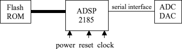
Figure 8.11 3-chip FIR processor with the ADSP2185N
Alternatively, the DSP may be connected to the bus of another processor via the 16-bit parallel host port which can also be used to transfer instruction codes and data to the internal RAM of the DSP before starting program execution on the DSP. Figure 8.11 shows the 218x based DSP system implementing an FIR filter and indicates how to connect a second DSP chip if more throughput is required. Note that a dual processor system based on the 2185N achieves the same processing rate and memory integration as a single 2191M processor with its simpler board level design, but consumes significantly less power due to the 0.18 μ technology and the simpler DSP architecture.
The 21xx has input pipelining registers to the MAC (MX0, MX1 and MY0, MY1), the ALU (AX0, AX1 and AY0, AY1) and the shifter (SI) that are explicitly addressed in the parallel load operation. Each unit also has separate output registers, MR (the 40-bit accumulator, further subdivided into 16-bit registers MR0, MR1 and MR2), AR and SR (SR0 and SR1), and extra 16-bit output registers AF and MF. The 219x substitutes MF with an alternative 40-bit accumulator. The output registers can also be used as input registers in chained calculations. Memory is addressed with 8 pointer registers I0-I7 that are incremented by the contents of update registers M0-M7 after every access (which is the only indirect addressing mode available), using modulo arithmetic to implement circular addressing. The circular buffer lengths are stored in extra registers L0-L7, and the 219x uses extra base registers for the start addresses. The instruction set supports load and store operations with their address updates in parallel to arithmetic.
For the FIR filter implementation, a single instruction is repeated in a loop performing the MAC operation and in parallel loading the operands for the next. Before entering this loop, the address registers chosen for the coefficients and the samples, I4 and I0, must be set to the starting addresses, and the address modifier registers must be set to 1. In assembly language, the loop then reads as shown in Listing 8.1.
(1) CLR MR, MX0 = DM(I0, M0), MY0 = PM(I4, M4);
(2) CTR = 511;
(3) DO L UNTIL CE
(4) L :   MR = MR + MX0*MY0(SS), MX0 = DM(I0, M0), MY0 = PM(I4, M4);
(5) MR = MR + MX0*MY0(RND);
(6) IF MV THEN SAT MR;
Listing 8.1 FIR loop for the ADSP21xx
As the loading of the multiplier operands into the registers MX0 and MY0 is pipelined, the first pair of operands must be loaded before performing the first multiplication. This is done in stage (1) in parallel to clearing the accumulator register MR to zero. ‘DM(I0,M0)’ specifies a load operation from the data memory using the address register I0 and incrementing I0 afterwards by the contents of M0. The zero-overhead loop is started by setting the dedicated loop counter register CTR and by performing the DO instruction that takes the address L of the final instruction of the loop body as its argument. After performing the MAC instructions in stage (4) in which ‘(SS)’ specifies a signed multiplication the final multiply in stage (5) does not load more operands, and uses the rounding option to convert to a 16-bit result. Stage (6) performs saturation in the case of an overflow. The rounded and saturated result of the length 512 FIR filter then stands in the ‘middle’ part M1 of MR. The circular addressing of the samples is implicit. After setting the buffer length register L0 to 511 during the program initialization, all further addressing with I0 is cyclic mod(512).
The FIR computation needs to be performed for every output sample and has to be synchronized with the input. Input comes from the A/D converter via a synchronous serial interface. The attached converter output the samples at the sampling rate to the DSP. The interface issues an interrupt for every received sample which can be used for the synchronization. A simple, single channel implementation could start by initializing the processor registers including L0, M0, I0 and M4 and the configuration registers of the serial interface to receive input words from the converter. The DSP then simply enables its interrupt and enters an idle loop. The interrupts cause this loop to be left for the interrupt processing and to be resumed afterwards. In the interrupt routine, the receive register is read, and the new sample is put into the cyclic buffer addressed by I0. Then the FIR loop is performed, and the result is written out to the transmit register of the interface. As the FIR computation has a constant execution time, the results are output at the sampling rate with a constant delay to the inputs.
Table 8.3 List of features for the TMS320C54x

8.4.2 The TMS320C54x Family
The TMS320C54x family from Texas Instruments has similar features (Table 8.3) but uses an implicit pipeline instead of input registers so that multiply instructions may directly specify a memory operand. Therefore only a few data registers are visible, namely two 40-bit accumulator registers A, B and an auxiliary input register T for the multiplier. Moreover, a second adder (a 40-bit ALU) can be used in parallel to the MAC operation in a special instruction called FIRS that takes a single cycle when it is repeated in a loop, and the memory organization allows two sample accesses and a coefficient read from an auto incrementing address to support the symmetrical FIR filter. The sum of two 16-bit samples occupies up to 17 bits in the accumulator, and the multiplier actually accepts a 17-bit signed input. A shifter is available, too, yet no logic to support block floating point. The TMS320C54x also offers a special instruction to speed up the Viterbi algorithm (cf. exercise 8). There is a broad choice of instruction rates ranging from 40 to 160 MHz and amounts of integrated memory, and there are versions integrating two DSP cores or a DSP core and an ARM processor.
Low cost processors of this series like the 100MIPS TMS320C5402 have an 8-bit host port only, while those with a 16-bit host port require the application of a DMA address. Comparing the 21xx to the 54x, the support for the symmetric FIR filter is a definite advantage for the TI chip, while for block floating point operations, e.g. in the FFT, the 218x has an advantage. For LMS filtering and the distance of vectors the 54x can employ its dual adders in parallel again. The 218x supports context switching and the control flow more efficiently, while the 54x has an edge in raw arithmetic performance. There is no clear winner; the choice to be made is application specific.
Memory is addressed with 8 registers AR0-AR7 that can also serve for loop counting. AR0 is also used as an index register. There is a unique stack implemented with a stack pointer register SP and residing in the data memory (in contrast to the separate, dedicated stack memory of the AD chips). Circular addressing is supported using a single block size register. There are a number of indirect addressing modes, some of which are shown in Table 8.4.
For the symmetric FIR computation, a third operand is needed and requires address generation. This is implemented in a special instruction and can only be used within a single-instruction repeat loop which cannot be interrupted. The instruction includes the absolute address of the coefficient array:
Table 8.4 Indirect addressing modes of the TMS320C54x (examples)
| *AR1 | operand at address in ar1 |
| *AR1+, *AR1− | same with address being post incremented or decremented |
| *AR1+%, *AR1−% | same using circular addressing |
| *AR1+0 | incrementing by ar0 |
| *+AR1 | preincremented address |
| *AR1(index) | index is a 16-bit signed constant added to ar1 before applying the address |
| *+AR1(index) | same with preincremented ar1 |
| *+AR1(index)% | same using circular addressing |
REPEAT#count
FIRS(* AR3 + %,*AR4 − %, #coeff).
8.4.3 Dual MAC Architectures
A recent derivative of the TMS320C54x architecture is the TMS320C55xx family. It achieves a still higher level of performance by increasing the instruction frequency up to 300 MHz and by providing more registers and two MAC circuits. There are four accumulator registers and four auxiliary registers. The 55xx series is a low power design. The lowest cost 5502 operates from a 1.26 V supply and integrates 64 k bytes of RAM. It is estimated to dissipate about 0.1 W at a 200 MHz clock rate. A version integrating an ARM core is used in a portable multimedia computer. The 55xx uses an instruction cache and decodes instructions of a variable size. The two MAC circuits may execute in parallel, e.g. to implement a two channel FIR filter (only 3 parallel data accesses are supported), or to calculate two subsequent outputs of the same filter. A two channel symmetric FIR filter is not supported as this would require an extra adder. Instruction set compatibility to the 54x family is maintained. On the 55x there is an extra address generator for the coefficient address, and single-instruction repeat loops are interruptible. The host port is 16 bit and can hence be used to build DSP networks. An important feature of the 55xx chips is the integration of an external memory interface that also supports synchronous DRAM (Table 8.5).
For applications of the TMS320VC55xx DSP family combined with an exposition of DSP algorithms we refer to [62].
A new, dual MAC integer architecture was recently developed by Analog Devices and Intel. The ‘Blackfin’ processor profits from a fast semiconductor process. It operates at 1.2 V and below and is offered at clock rates of 400 and 600 MHz. In FIR algorithm, it hence achieves 800 or 1200 16/40-bit MAC operations/s. As a remarkable feature, the Blackfin integrates a software-controlled switching regulator that delivers a programmable voltage between 0.7 V and 1.2 V to the core. The clock of the core is generated by a PLL circuit and is under software control too, so that the power consumption can be adapted to changing requirements. The Blackfin shares some feature otherwise found on micro controllers (e.g. special timer functions) and on general-purpose processors that enable it to use some of its resources for general-purpose computing and to run an operating system. In particular, it offers a ‘supervisor’ mode and a memory management unit. Instruction lengths are 16- and 32-bit, and an instruction cache delivers them fast enough to support their parallel execution. There is a data cache too, or a configurable mix of on-chip RAM and caches (a total of 148 k bytes on the ADSP-BF533). The processor uses 16 16-bit data registers and eight address registers and related modifier registers like the 219x family, and some extra address registers used for non-DSP HLL programs. Besides the usual synchronous serial ports it also includes a port for video data and provides special instructions for such. The external memory interface of the Blackfin uses a 16-bit data bus and also supports SDRAM. The Blackfin comes in a tiny, 160-ball BGA package.
Table 8.5 List of features for the TMS320C55xx processors

Besides the dual MAC chips there are some that even offer 4 MAC operations per cycle. A fast, integer DSP from Lucent and Motorola is the Star Core DSP. The basic core integrates 4 MAC circuits and runs at 300 MHz executing several 16-bit instructions in parallel. The MSC8101 also packs 512 k bytes of RAM and a number of peripherals and dissipates 2/3 W. Another version, the MSC8102 even integrates 4 cores and thus performs 16 MAC operations per cycle. Another very fast integer DSP is the TMS320C64xx from TI. It also performs 4 16-bit multiply operations per cycle and runs at still higher rates of 720 MHz and beyond. This architecture is related to the TMS320C67xx architecture that will be discussed in section 8.5.2.
We finally mention the MC56321 DSP from Motorola, the latest offspring of a DSP family introduced in the late 1980s. It differs from the integer DSP chips discussed so far by implementing a 24-bit integer type, using a 24 × 24 bit multiplier and a 56-bit accumulator. The 24-bit data type is convenient for audio processing applications that often require more dynamics than provided by the 16-bit range. This processor core performs 240 MIPS consuming about 0.4 W from a 1.6 V supply. The chip is housed in a 196-pin BGA and integrates nearly 600 k bytes of SRAM. The processor supports block floating point operations and executes an FFT butterfly in six cycles. The MC56321 also includes a second MAC circuit but uses a different approach to support it. The second 24/56 bit MAC is part of a preprogrammed filtering coprocessor that can be used for a selection of standard filtering algorithm including the FIR computation. Together, the processor and its coprocessor execute 480 million 24-bit MAC operations per second during FIR computations.
8.5 FLOATING POINT PROCESSORS
Floating point DSP chips use some of the standard 32-, 40- or even 64-bit formats and implement the basic arithmetic operations +, −, * for these with parallel or pipelined, high-speed circuits, typically executing them with a single cycle throughput. They are more complex and costly and are typically used for complex algorithms where the accumulation of rounding errors and overflow would be hard to handle in fixed point. They also offer an easy way to port DSP algorithms developed on a workstation with floating point arithmetic to a real-time environment without having to think about fixed point effects which has become a common design practice.
An important benchmark for floating point DSP is the FFT. As the butterfly is the basic building block of the FFT, an approach to building a fast FFT processor would be to provide a parallel circuit for the butterfly, attach multiple memories and address generators to it for parallel input and output, and to use a sequencer to control the repeated usage of the circuit. Chips of this kind have been on the market, but this structure is highly specialized and expensive due to the multiple memories. For a standard chip serving many applications, a processor architecture with a single floating point multiplier is more flexible. As the butterfly contains 4 real multiplies, the multiplier would be applied 4 times per butterfly computation. The FFT would run effectively if the 6 add and subtract operations and the 8 i/o load and stores could be performed in parallel to the multiplications. This amounts to two load and store operations in parallel to the arithmetic operation which is more moderate and similar to what is needed for the FIR computation. In fact, one cannot do better. The performance of the parallel butterfly circuit performing 4 multiplies per application is also obtained by using 4 single multiplier processors performing a butterfly in 4 multiply cycles each. These perform 4 butterflies in 4 cycles and make 8 parallel memory accesses per cycle similarly to the dedicated structure. If only the FFT were concerned, they might share the control circuit.
8.5.1 The Sharc Family
The Sharc family is a family of floating point DSP chips from Analog Devices. The Sharc architecture is similar to the ADSP218x architecture in several respects yet doubling most of the resources found there. It provides separate multiplier and ALU circuits but instead of the dedicated input and output registers found in the ADSP218x uses a uniform set of 16 data registers that can be used with all arithmetic operations, and additional addressing modes. These features were later implemented on the 219x processors, too. The Sharc CPU executes 40-bit floating point operations and stores floating-point data in 40- or 32-bit words. It also supports a 32-bit fixed point data type and provides a MAC structure with an extra adder and two 80-bit accumulator registers for this. As a special feature related to the FFT, the ALU performs a parallel add and subtract operation on the same inputs that can be used in parallel to a multiply as needed for a four cycle butterfly. In contrast to the 218x the Sharc performs one memory access per cycle from its program memory bus only. This is compensated for by providing a tiny instruction cache. A strange side effect of this is that instructions with two parallel data accesses execute twice as fast from a loop as from a linear, unrolled program.
The Sharc instructions have a fairly large width of 48 bits and support various parallel operations of the computational circuits, e.g. a MAC operation and a simultaneous ALU operation with independent addresses for five involved registers in parallel to single or dual data moves for another two registers. The only flaw is the lack of being able to address the second accumulator registers in combined MAC and ALU instructions which would allow efficient implementation of the symmetric FIR filter. The multifunction instructions used in the FFT butterfly e.g. perform a floating point multiply operation in parallel to a single add operation or to the 2-input DFT operation (the parallel add and subtract) and two memory accesses. A single instruction of this kind reads:
![]()
Individual MAC or ALU operations with parallel data moves may be conditional. Arithmetic overflow and floating point exceptions may generate interrupts (cf. section 6.4).
As already pointed out in section 7.1.3, the Sharc architecture has the unique feature of defining and implementing special networking interfaces, the Sharc links. In the second Sharc generation, the link ports have been extended to transmit 8 bits per clock instead of 4 in the first generation. They can, however, still be configured to use just 4 and to interface to first generation processors. Unfortunately, compatible links ports are not available on other (16-bit) processors to allow for heterogeneous networks.
The data in Table 8.6 hold for the ADSP21161 already mentioned there, a member of the second Sharc generation with a 32-bit external bus interface offering all support function (refresh, strobe generation, address multiplexing) necessary to directly connect to SDRAM chips for the low cost and high density external expansion of its memory. If the link ports are not used, 16 additional data bus lines become available. In the first generation, only the low-cost 66 MHz ADSP21065 without link interfaces and just 64 k bytes of internal RAM offers SDRAM support. The ADSP21065 consumes 1W from a 3.3 V supply. Another important feature in the first and second Sharc generations is that the internal RAM is dual ported and can be independently accessed at full speed from both the CPU and the DMA circuits.
The second generation processors use two identical sets of compute circuits that operate in a SIMD fashion, i.e. execute the same instructions which may, however, be conditional. This can be exploited in the common case of the same DSP algorithm being applied to several, independent data channels, e.g. processing left and right audio channels, or the half size DFT applications in the DFT factoring (otherwise, one of the compute section is not used at all). The SIMD processing requires independent data to be delivered to both compute sections, i.e. 4 parallel operand accesses per cycles. This is implemented by providing internal memory widths of 64 bits and storing the independent data in the upper and lower halves of the same 64-bit words. No extra address generators are needed this way, and the instruction set remains the same. The ADSP21161 fabricated in 0.18 μ technology achieves three times the performance of the 21065 but only slightly increases the power consumption.
Recently, the 2nd generation Sharc architecture has been reimplemented in a 0.12μ process. The ADSP21262 doubles the speed and the on-chip memory of the ADSP21161 yet consumes half the power. This chip, however, lacks the SDRAM support and the link and host interfaces (and comes in a 144-pin QFP package).
There is a follow-on to the Sharc, the so-called Tiger Sharc architecture. The arithmetical circuits are further extended. There remain two identical compute sections with a 32-bit multiplier in each one. The Tiger Sharc is more universally applicable by supporting 16- and 32-bit fixed point data at the same level of efficiency. It does so by rearranging the ALU and MAC circuits to allow several 16-bit operands in parallel. Each of the MAC circuits can perform 32-bit multiplies with 80-bit accumulation or in parallel 4 16-bit MAC operations with 40-bit accumulation, or complex 16-bit multiplies. In contrast, the previous Sharc processors would support 16-bit operations at the same rate as 32-bit data, leaving 75% of the multiplier circuit unused. Floating point operations do not benefit from this feature; the performance remains at 2.5 operations per cycle for the FFT. However, on the Tiger Sharc SIMD processing now becomes an option; the parallel usage of the compute sections is also possible with independent instructions, and more algorithms can exploit both compute circuits. Also, a larger set of registers, namely 32 32-bit registers per compute section, is provided. The dedicated address generators are replaced by integer ALU circuits that are used in parallel to the compute sections. Up to four instructions, one for each of the compute sections and integer ALUs can be executed in parallel, similarly to executing a VLIW instruction. The internal buses are 128 bits wide and allow 8 operand fetches per cycle. The restriction remains that only two addresses are generated in parallel. Multiple operands must be in consecutive locations. The internal memory is no longer dual-ported but provides a third bank that can be accessed by the DMA circuits while the CPU is accessing the other two. The Tiger Sharc processors run at faster clock speeds and use faster link ports that are no longer compatible with those of the former generations. Table 8.7 lists some data that hold for the TS101. The TS101 improves the power efficiency by a factor of two over the second generation. The Sharc family offers the option to achieve the same floating point performance with three interconnected second generation processors too. The TS101 processor achieves about the same performance on an FFT (about 30 μs for a 1024 point complex FFT) as the 1GHz MPC7447 with its vector processing unit. The latter, however, dissipates five times the power and needs an additional ASIC to interface it to an EPROM and to converters for stand-alone operation.
Table 8.6 List of features of the ADSP21161

Table 8.7 List of features of the TS101
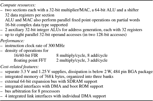
The most recent TS20x chips operate from 1 V and raise the clock rate further to 500 MHz, replace on-chip SRAM by on-chip DRAM, and use LVDS link signals. The lowest cost TS203 provides two links only, and 512 k bytes of RAM while the TS201 integrates as much as 3 M bytes of RAM. They are housed in 576-pin BGA packages.
8.5.2 The TMS320C67xx Family
The TMS320C67xx family from Texas Instruments represents a VLIW architecture (see section 6.6.4) with eight functional units executing individual instructions in parallel. The eight units break up into two identical sets each containing a 32-bit multiplier M, an ALU L performing adds, subtracts, comparisons, conversions and bit field operations, a shifter unit S also performing add, subtract, floating point divide and compare operations and branch instructions, and an address calculation unit D performing load and store operations and add and subtract operations on address codes. Each set connects to a bank of 16 32-bit registers of its own, the A and B register files. The L, M and S units can access a single operand from the other register file per cycle as well. For a 16-bit MAC operation, one would use the M and L units in a pipeline and specify the 40-bit add operation on L. While the L, S, and D units can be used for fixed point add and subtract operations, floating point add and subtract operations only execute on the L units. The 67xx has the unusual feature of also efficiently supporting the 64-bit, double precision floating point type at ¼ of the single precision rate, and addresses memory by bytes. It uses a pipeline with 7 to 16 stages including 1-9 execute stages depending on the operation.
Table 8.8 Assignment and scheduling of operations

Usually, the compiler selects the operations that are executed in parallel on the different compute circuits. Assembly level programming is more difficult than for scalar and superscalar architectures as the pipeline of the processor and the parallel scheduling must be taken care of. As an example, the operations of loading two 16-bit samples from memory, multiplying their scaled sum by a coefficient also loaded from memory, and adding the multiply result to a register used as an accumulator could be arranged as shown in Table 8.8 using minimum delays. The delays after the load and multiply instructions are needed due to their extra processing time. The free time slots and unused units may, of course, be filled up with interleaving and parallel operations. Care must be taken not to use a register as a data source during the delay following an instruction that changes it. An intermediate interrupt might cause the change before this use. The up to eight instructions in a row are marked to be executed in parallel and constitute execute packets of up to 256 bits that are loaded in parallel from the instruction cache. There is no instruction for a single-cycle 17 × 16 bit multiply or for a single cycle combined add and divide by two. Therefore the ‘shr’ instructions cannot be avoided, and the symmetric FIR filter cannot be computed efficiently using both multipliers, one of the compute units being needed twice in every step. Only TMS320C64xx provides a fast 16 × 32 bit multiply operation.
Branches are delayed, too, and become effective after 5 cycles only. During this time, interrupts are automatically disabled. All instructions including the branch instructions are conditional. If e.g. some composite operation is carried out on all components of a vector, one would first fill up execute packets of parallel operations on subsequent vector components (unrolling a preliminary description of the vector operation as a loop), and only then identify a periodic section of the assembly program. This is used to set up a loop, using one of the S units to maintain a counter and carry out the branch instructions in parallel to the other units. At least 6 cycles must be executed in the loop body (the branch execution time). The branch conditions do not refer to a status register but test some general register to be zero (or non-zero). Comparisons place their Boolean result (0 or 1) into a register. There is no overflow indication for integer add operations. Calls to sub-routines must be implemented as unconditional jumps, placing a load program counter instruction into the last execute packet before the branch is taken. The encoding of the parallel operations of the circuits by individual 32-bit instruction evidently requires much memory. An efficient FIR routine performing two loads, a multiply and an add operation requires 128 bits of instruction code for these, and an FIR loop contains at least 24 instruction words.
The computational resources of the 67xx are not too far from the multiplier, ALU, shifter and address generator circuits found in other DSP chips as well. The eight units are, in fact, similar to the parallel circuits in the second Sharc generation. The independent programmability of the two sets and the usability of the address generator unit for general purpose computations are only available on the Tiger Sharc. The 67xx lacks the high i/o bandwidth of the Sharc processors due to their parallel DMA accesses, their FFT efficiency by a factor of 2, and the support for accumulating integer products to 80 bits, their code density, and the efficiency on 16-bit data of the Tiger Sharc, but does provide the double precision floating point and the character data types that may be useful in some applications. Comparing the low-cost TMS320C6713 to the second generation of Sharc processors, in particular to the ADSP21161, the more advanced manufacturing technology (0.13 μ), however, leads to higher clock rates, to more performance in non-FFT applications, and to a better power efficiency. While the second generation Sharc processors can use their second compute section only for SIMD operations, the VLIW structure has no such restriction. The TMS320C6713 integrates more memory than the ADSP21161 and provides an easier host interface. Its main features are shown in Table 8.9 for the low cost QFP package version. The ADSP21262 is an obvious competitor. Another competitive device to the 6713 might be the SH-4 (see section 6.6.4) in some applications.
The TMS320C67xx family also lacks a networking concept for the use of the processor as the compute node in a scalable architecture. This has to be added at the board level, using e.g. an FPGA to implement fast LVDS interfaces, or some dedicated extra chip, disadvantages being the higher costs and the non-existence of an architectural standard.
Table 8.9 List of features of the TMS320C6713
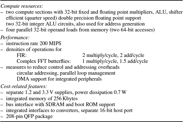
8.6 DSP ON FPGA
The FPGA discussed in section 2.2.4 as a configurable hardware platform allowing the realization of application specific processors and even networks of such may also be used to implement FIR filtering and other DSP algorithms. The fast serial MAC structure explained in Chapter 4 is easily implemented in several instances on an FPGA along with the necessary control circuit. The RAM blocks found in recent FPGA chips may be used to store coefficients and samples; otherwise an external memory chip would need to be interfaced.
For look-up table-based FPGA architectures the constancy of the coefficients can be used to implement FIR segments of 4-6 multiply-add operations using distributed arithmetic (section 4.5) which significantly decreases the complexity and increases the processing speed in comparison to an implementation of individual parallel multipliers. Longer FIR filters can be subdivided into short blocks implemented this way.
FIR processing can also be implemented by subdividing the filter into short ones and performing the processing with these by blocks. After processing a block of samples with the short filter, the look-up tables can be overwritten for the next filter section. This is equivalent to partially reconfiguring the FPGA for different steps, buffering the intermediate data in a memory. This technique can actually be applied to all kinds of DSP algorithm having only a throughput requirement.
Finally, the Virtex-II and Spartan-III families from Xilinx include 18-bit parallel multiplier blocks and RAM to build various DSP-related data paths and to implement even very high speed filters. Altera's Stratix devices go even further by including the MAC function and some configurability. The required sequential control is easily implemented on the FPGA so that the equivalent of multiple specialized DSP processors can be mapped onto a high density FPGA. Then all kinds of algorithm-specific building blocks (cf. section 8.2.4), including the full butterfly structure, can be realized on the FPGA and be used sequentially as application-specific compute circuits receiving multiple input data per cycle from separate memory blocks.
It is evident that with this inventory of methods the FPGA equipped with additional memory becomes a strong alternative to dedicated processor chips, in particular if appropriate tool chains are available to simplify the programming. Due to their configuration overheads FPGA-chips are more expensive than processor chips produced in mass volume, but further architectural advances in FPGA will increase the share of FPGA-based DSP designs, which in turn will contribute to driving down the FPGA prices.
8.7 APPLICATIONS TO UNDERWATER SOUND
In this final section, we analyze some sample applications arising in the field of underwater sound for their computational requirements and outline appropriate system architectures for them on the basis of the techniques seen before. Besides the involved signal processing algorithms, the handling of the involved data rates and the memory requirements need to be considered. This is quite typical for high speed DSP applications which may require special interface and buffer memory designs attached to the processors, in particular, if many signal channels and 2D storage are involved.
In the sea, vision and object detection, communications, and distance measurements are by means of acoustic signals. Electromagnetic waves are damped too much to serve these purposes. Sound travels through water at a velocity c of 1495 m/s at the temperature of 20°C. It is sent out unintentionally by moving vessels, and intentionally by means of piezoelectric transducers at frequencies up to a few hundred kHz. Sound can be received by underwater microphones (‘hydrophones’). The transducers used for the generation of sound can also be used as hydrophones. The attenuation of a sound wave traveling through the water grows with its frequency. At low frequencies, directed sound beams can be registered over tens of miles. Narrow sound beams are generated by wide, flat transducers, while small transducers act as omni-directional point sources. If the same transducers are used as hydrophones, they have similar directional characteristics.
A classical application of underwater sound is the echo sounder used to measure the water depth d beneath a vessel. A sound pulse is transmitted against the sea floor, and the echo from the sea floor is registered afterwards. The time t between sending the pulse and receiving the echo is given by the formula t = 2d/c as the sound has to travel down and up again. Fish schools can also be detected by their echoes. The transmitted signal can be synthesized by a DSP, and the received signal can be digitized and evaluated by means of a DSP as well. The same applies to communications through the water by means of modulated sound signals, and to passively listening for approaching vessels. Sonar signal processing can be further studied in [64].
8.7.1 Echo Sounder Design
A modern ‘vertical’ echo sounder based on a digital processor is required to perform some or all of the following tasks. The basic structure of the measurement system into which the digital processor is embedded is shown in Figure 8.12. The measurement system is further embedded into its physical environment including the water and the seafloor reflecting the sound. An echo sounder can do the following:
- periodically perform a measurement by outputting a trigger pulse to a transmit circuit, or even a synthesized waveform to be amplified and sent out, and control the amplifiers;
- acquire the echo signal from a hydrophone amplifier;
- display the signal on an LCD screen;
- detect the echo from the sea floor and calculate the water depth;
- scan the user interface (a keyboard) and input measurement parameters;
- interface to a printer, a GPS system, to a remote computer, and to depth displays;
- perform data logging to some storage device.
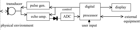
Figure 8.12 Echo sounder system

Figure 8.13 Echo amplitude after the pulse and echo display
In order to determine the performance required from the digital processor, the amount of memory and its interfaces, the measurement parameters and the algorithms to be implemented have to be specified. Typical measurement parameters for a shallow water echo sounder would be:
- depth ranges of 25 m, 50 m, 100 m, 200 m;
- measurement cycle times of 50 ms, 100 ms, 200 ms, 400 ms accordingly;
- bandwidth and dynamic range of the echo amplitude signal are 5 kHz, 40 dB.
A simple algorithm to determine the water depth, assuming a trapezoidal shape of the bottom echo, is to determine the maximum echo amplitude over the full range and to search for the time when some fraction of this level was reached first (Figure 8.13). Typically, a design project would not specify such a procedure in detail but rather some performance and cost levels and only some details concerning the user interface and the external interfaces, and leave it to the engineer to set up an adequate model of the measurement process. For the specific example of a low-cost, portable echo sounder the screen might e.g. be required to display 240 × 180 single bit pixels, and a single serial interface outputting the water depth as a string of characters after every measurement might be asked for.
From the above givens one concludes that an 8-bit converter can be used at a sampling rate of 15 kHz (somewhat larger than 2 * 5 kHz); in principle, there is the more costly option to digitize the AC echo signal and to perform the rectification and the smoothing digitally. The range of 25 m nicely translates into a set of 500 samples taken after the transmit pulse. As the resolution of the measurement and the display will not depend on the range, the digital processor may compress the samples to a set of 500 in all ranges. The video memory is required to have a size of just 5.8 k bytes. A typical signal display results from mapping the amplitude values from subsequent measurements to adjacent lines of 240 pixels, scrolling the display down so that new lines are always added at the top. Then the shape of the sea floor can be read off the display (Figure 8.13). The input signal is thus displayed as a 2D signal that is acquired serially line by line. We assume that the video signal will also be serially output line by line, as a bit sequence along with a clock and sync signals, similarly to the pattern in which the samples were originally input (but much faster).
The measurement needs to be repeated as the ship moves on. It constitutes a sampling of the bottom shape and must be repeated at subsequent positions of the ship in relation to the ‘bandwidth’ of this shape along the track. The measurement rate must be in proportion to the ship's speed. The maximum rate is usually limited so that the echo acquisition times for subsequent measurements do not overlap. In the 25 m range, the fastest rate would e.g. be set to 50 ms. This is hence the maximum available time to evaluate a measurement. For larger ranges, this time is longer (it might be used for a more elaborate evaluation). Usually, the measurement rate is not adapted to the speed and to the bottom shape at all so that the bottom shape is greatly over-sampled. The subsequent measurements are useful to provide more data to compensate for flaws in the individual measurements due to the changing acoustic conditions that may lead to echo losses, changes of the echo amplitude, and erroneous echoes from objects other than the sea floor.

Figure 8.14 Processes in the digital system
In order to define the computational task of the depth evaluation, it is useful to look at it as an inverse scattering problem. The environment (the water space and the sea floor) is probed with the echo pulse and responds by an echo from which structural parameters of the environment are derived. For this purpose, a simple physical model of the environment and its result on the echo are set up. The echo evaluation adjusts the parameters of the model so that it yields the best approximation of the actual echo. The quality of the depth evaluation depends on the quality of the physical model. If the sea floor is modeled as an ideal reflecting plane parallel to the water surface at the distance d, then the parameter d can be derived as above. A refined model would take care of the inclination of the sea floor and its structure and be adjusted through a series of measurements.
It is only after these considerations that the basic processes of the digital processor can be defined (Figure 8.14). The steps involved are a repetitive process reading the user settings and starting the measurement by sending out the stimulus to the environment at the required rate, a process inputting and compressing the echo samples (the response to the stimulus), an evaluation process, and a video process to refresh the display. The response acquisition process takes the maximum of some subsequent samples and otherwise just writes the preprocessed samples to a memory buffer. The matching process served to evaluate the individual measurements. It further compresses, packs and passes the samples to the video RAM, and proceeds to the bottom detection by matching the model parameters to the received echo shape. For the simple, behavioral echo model this requires two comparisons per sample. Even with some more preprocessing of the samples and some smoothing of the results, the effort remains small.
Once the processes are defined, the computational requirements can be estimated. Every 8-bit micro controller can perform all of the operations required for the echo acquisition and evaluation and even allows for a more sophisticated evaluation using a refined model. The sample input at the 66 μs rate can be realized as an interrupt process in parallel to the evaluation of the previous data.
The video output process with its scrolling operation is the only process that requires a higher rate of operations. At a refresh rate of as low as 50 ms, the pixel output rate is about 1.5 MHz. Here, some hardware can be implemented that cyclically sends out the memory contents (or a standard display controller chip). A line of 240 pixels can be stored in 32 adjacent bytes of an SRAM to facilitate the 2D addressing by lines and columns. The scrolling can be realized by changing the start position for the sending to some multiple of 32 bytes and by using a cyclic addressing scheme for the readout and the inputting. Thus, this process can be realized using a RAM controlled by an FPGA or PLD circuit interfaced to the micro controller. An At94 k chip e.g. has all these ingredients including the memory and the serial interface and only needs a serial Flash memory for the application code and an ADC but it does not yield the cheapest solution.
If the video output is replaced by a numeric display, the application would be conveniently served by any micro controller with an integrated ADC, a timer to generate the sample rate and a serial interface, e.g. an AVR chip or the MSP430 that also include the program ROM. If more interfaces and functions were required, a more complex micro controller would be used. Only for operations on the AC echo signal a DSP chip would be required and be used stand-alone or in conjunction with a micro controller.
The basic echo sounder function can be refined in various ways in order to enhance the sensitivity and the quality of the measurements. One is to send out a long, modulated pulse (synthesized by a DSP) with a sharply located autocorrelation. The received AC signal is sampled and correlated with the sent out waveform in order to undo the echo lengthening due to the long pulse. At a sampling rate of e.g. 100 kHz and a pulse length of 5 ms, the correlation is equivalent to performing an FIR computation of the length 500 which can be handled by any single MAC integer DSP at 50 MIPS.
8.7.2 Beam Forming
The directionality of an extended, flat transducer used as a hydrophone results from the voltages at the different surface elements, only summing up constructively if they are excited in phase, and a directional beam forms from the transmitting transducer as the spherical wave fronts issued by the surface elements are superimposed constructively far from the transducer in the forward direction only. Electronic beam forming is based on subdividing the transducer used as a hydrophone into multiple elements, the signals of which are processed separately and only summed up electronically. The signals are sampled, buffered, and summed up with individual delays so that the constructive summation only occurs for input beams from an angle of φ w.r.t. the forward direction (Figure 8.15). If d is the distance between two elements, then the delay h to be applied is related to φ by the equation:
![]()

Figure 8.15 Time delay of the signals from two hydrophones
For a sine wave with the frequency f the delay h translates into the phase shift of ψ so that:
![]()
To form a directional beam from an array of N hydrophone elements, one has to calculate the sum
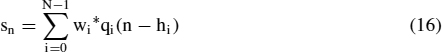
where qi (m) denotes the mth sample from the ith hydrophone, and hi is the delay to be applied to it in units of the sampling period and wi is a windowing coefficient used to improve the directional characteristic and to compensate for the directional characteristic of the individual hydrophone, if necessary. A 2D storage structure is needed to store the qi(m). If qi(n − hi) is linearly interpolated from two adjacent samples (more are needed at low sampling rates), then 4N operations are needed to compute equation (16). The hydrophones do not need to be arranged linearly. An arbitrary arrangement can be used by properly adjusting the time delays hi, e.g. a circular array. Also, the sampling of the hydrophones does not need to be simultaneous. Apart from the interpolation errors, equation (16) does not depend on the frequency of the signal. For low frequencies one obtains a broader directional characteristic.
For a narrow band signal centered on a frequency f time-domain beam forming equation (16) can be substituted by frequency-domain beam forming, i.e. by multiplying the complex signal sample pairs qi(n) = (rqi,n, iqi,n) taken as in Figure 8.2 by phase factors pi = exp(−j*ψi), j being the imaginary unit and ψi = 2πf * hi. The computation thus becomes

and is easier to implement as it no longer involves the addressing of samples at different time positions. The operation of forming the qi(n) from the sample pairs can be combined with equation (17) by adjusting the coefficients and thus costs no extra effort. To send out directional beams, the individual elements are excited with the negated time delays or phase shifts.
Electronic beam forming can be used to stabilize the receive beam of a vertical deep water echo sounder against the roll motion of the ship. Sharp beams need to be used to increase the sensitivity for the weak echoes, and during the time the echo travels through the water the roll angle may have changed by several degrees. If a linear arrangement of 32 transducer stripes is used that are spaced by a quarter of the wavelength and if the sampling frequency is 80 kHz, then equation (16) requires 64 operations to be performed within 12.5 μs, i.e. 5 per μs, well within the reach all the current signal processors. 32 × 32 memory locations are needed to generate the time delays to sweep the receive beam by ±90°. Vertical echo sounders use narrow band pulses and can apply phase beam forming, as well.
Still more interesting is the observation that from the same stored samples not just one but several different directional beams can be formed. This is exploited in the multi-beam echo sounders that are used to perform depth measurements not just beneath a surface vessel but also at some distance to its path, using directional beams sent out at up to 60° from the vertical direction. There is still enough echo energy coming back out of these directions to permit a distance evaluation. Multi-beam echo sounders are used to scan the sea floor in harbors and rivers quickly and to derive charts of the bottom from these. As a second example, we estimate the computational requirements for a 20 kHz multi-beam echo sounder using two arrays of 32 transducer stripes each mounted on both sides of a ship (at angles of ±30° to the vertical) and simultaneously sending out and receiving fans of four beams each. The depth data are sent out via an interface to a standard computer to store them along with the positional data for later processing and to immediately display and optionally print them as a chart of the region beneath the ship covered by the measurements. Additional interfaces are needed for the roll angle and other sensors. In this case a narrow band signal is sent out so that phase beam forming can be used. Using quadrature sampling the sample rate can be reduced and will be assumed to be 20 kHz.
The process structure of the single beam echo sounder shown in Figure 8.14 remains valid except for the video output process. The acquisition process needs to be extended by a digital phase shift beam former function. It receives more input samples at a higher rate, namely a stream of 2*32 complex input sample pairs (gi, hi) taken in parallel at a rate of 20 kHz and transforms it into a stream of sets of 8 complex samples at the same rate. These need to be rectified (taking their absolute values) and compressed to fill the input buffers for the depth evaluation. The depth evaluation process evaluates all of them one by one. The stimulus process generates the parameters for the 8 stimuli used within a fan of simultaneous beams. Each transducer array uses a multi-channel pulse generator that generates the delayed signals for the transducer elements from a pre-computed wave table according to the givens from the stimulus process for each of the four directions in sequence.
The beam former needs to perform 128 real MAC operations every 50 μs for each of 8 beams, i.e. perform about 20 million MAC operations per second. The result rate is still high at 640 k samples per second, i.e. before the demodulation and compression are applied. The computation can be performed by several of the DSP processors previously described. In order to reduce the data rates before communications to another processor occur, it is convenient to also perform demodulation and compression on the same DSP, i.e. the entire acquisition process, and to provide the buffer memory required for the 8 channels to it. A DSP chip capable of operating even faster than the required total rate and equipped with enough on-chip memory is the ADSP2191. It can take over the depth evaluation as well.
The ADSP2191 can receive the input samples from the amplifiers in the two transducer arrays via its two synchronous serial interfaces. This requires fast converters to be attached to the amplifiers that present the samples from the 32 channels as a single serial data stream (that may be transferred from the amplifier units to the DSP board using fast drivers, e.g. LVDS). In order to avoid an extensive context switching on the DSP, the stimulus process can be executed by an extra micro controller like the XC161 which also provides interfaces for the sensors and to the standard computer, and integrates the program storage for the total system. Both processors could be mounted on a single small circuit board, and the XC161 would communicate with the 2191 via the host port of the latter and download the DSP program to it when the system is started. Alternatively, a single highly integrated processor with DSP and controller features like the Blackfin could be used. A similar system designed in the late 1980s required six processors and dedicated hardware for the beam former on several complex circuit boards.
8.7.3 Passive Sonar
As a final application involving an FFT-based 2D signal analysis we consider the passive sonar that does not send out stimuli to the environment but simply analyzes the sound received via a large array of hydrophones. These are found on submarines where they are used to detect the approach of vessels, and to supply the data to distinguish between harmless and dangerous objects. As a typical sonar hydrophone array we consider a circular array of 96 elements that are continuously sampled at 40 kHz to cover a signal bandwidth of 15 kHz. These data are evaluated through the following steps:
- Subdivide the signal input using a bank of narrow band pass filters (about 100 Hz width).
- Form multiple beams by applying a phase beam former to the individual bands.
- 2D display of the signals by directions and frequencies.
- Detection and tracking of targets, and classification.
We concentrate on the directional and frequency analysis steps that also require attention for the involved memory design. The further processing to track and classify some small number of targets proceeds at lower rates.
The filter bank is realized by applying a 1024-input windowed FFT to every channel. The individual FFT outputs are spaced by 40 Hz. The FFT is computed with a 50% overlap (this is just enough for a bandwidth of 80 Hz and sufficient for the further processing), i.e. every 12.5 ms. In total, this amounts to computing a real 1024-input FFT every 125 μs. A single 100 MHz ADSP21161 can achieve this in half of this time. If every second FFT coefficient is used as a filter, the filters are centered on the multiples of 80 Hz.
The total input sample rate is 4 samples per μs. The samples are received serially in blocks of 96, each block containing a sample from each beam. They need to be stored by columns in a 2D memory of 96*1024 words and moved out by rows of 1024 to perform the FFT processing on the individual hydrophone channels, the rate being of 8 samples per μs as every sample is used in two FFT calculations. The results of these FFT evaluations repeated every 12.5 ms are 96*1024 complex numbers, of which just 96*192 have to be moved into another memory buffer as the desired filter outputs in the range of up to 15 kHz. The total data rate for this is 4 words per μs.
The samples can be entered via one of the link interfaces of the Sharc processor which also facilitates the synchronization of the FFT processing with the data input. During the 125 μs available for every FFT 480 new samples come in and can be buffered on-chip first (alternatively, one might e.g. choose to process blocks of 16 FFT computations every 2ms receiving 7680 samples during this time). The memory buffer can be realized by attaching an SRAM of 256 k 16-bit words to the Sharc bus that can be accessed at a peak rate of 50 MHz and is large enough to hold 1024 FFT input samples for every beam and the new samples arriving during the current 12.5ms of FFT processing. Moving in the 1024 samples for an FFT takes 20 μs, and moving out the new samples received via the link takes 10 μs as well. The filter outputs are 384 real words that are moved out in another 8 μs, too, into some double SRAM buffer of 128 k 16-bit words. The data are moved via DMA to the dual-ported internal memory in order not to lose the 40 μs required for them for the processing.
For the directional analysis, a set of 96 narrow beams are formed around the circle. For each of 192 frequencies, the complex FFT outputs hi,f of 32 adjacent hydrophone channels are weighted with amplitude and phase factors pi,f and summed up to form the signal energy according to the formula:

The beam former implementation becomes particularly simple in the special case of a circular array on which the hydrophones are regularly and precisely adjusted at angles of k*360°/96. Then the coefficients in equation (18) are actually the same for all beams at the fixed frequency f, and the sums in equation (18) are obtained from a circular convolution of the 96 element hi,f sequence, or of this sequence extended to 128 elements and a fixed coefficient sequence of length 32. It can be computed by applying a 128-input complex FFT to the hi,f sequence, multiplying by the transformed coefficient sequence and then applying the inverse FFT. The total computation must be performed for 192 frequencies in 12.5 ms, i.e. in 62.5 μs per frequency. The ADSP21161 performs the 128-input FFT in less than 10 μs and hence the beam forming in less than half the required time. Thus a single ADSP21161 can be used to both perform the 192 band pass filters and the beam forming.
The beam forming becomes much more complex if a non-circular and even non-symmetric array is used, and equation (18) must be computed with individual coefficients for every beam and every frequency. The direct computation of equation (18) amounts to 192*128 real MAC operations that need to be performed every 12.5 ms and for 96 directions. In total, these are nearly 200 million MAC operations per second, and 100 million coefficients need to be provided for these. In view of the available networking interfaces we continue to consider the ADSP21161 as an architectural component. Without the required initializations and the squaring operations in equation (18), the MAC operations nearly exhaust the processing capabilities of another ADSP21161 chip and are therefore distributed to two such chips. The coefficients cannot easily be computed at the MAC rate from more compressed geometrical data and need to be obtained from a memory table (the table data may initially be computed from geometrical data). Thus 1.2 M words of coefficient memory are required where real coefficients can be loaded at a rate of 100 MHz.
If the beam processing is carried out by columns containing the 96 filter outputs of all beams at a particular frequency f, that are transferred to the internal memory of a processor before performing the beam forming on them, about 4 words per μs need to be read out again from the memory. The results of this processing are 192 energy levels for each of 96 beams that are obtained every 12.5 ms. They fill up another 20 k words of memory and need 4 accesses per μs if they have to be stored and loaded again before they are moved to the display. This output can occur via another Sharc link. The total required memory is thus less than 2M 16-bit words. The total access rate is 124 accesses per μs. A structure of this kind is obtained by connecting the ADSP21161 chips via a common bus and attaching SDRAM at a width of 32 bits to it (Figure 8.16). These can be accessed at a rate of 100 MHz using page mode accesses and DMA to the internal Sharc memories. The use of SDRAM requires the mentioned block processing alternative for the FFT in order to be able to perform page mode accesses to the 2D memory all the time.
With some extra effort for the interfacing and by carefully checking the memory band-widths, the two Sharc chips used to the beam forming could be substituted by a single, high-speed dual-MAC integer DSP as equation (18) only involves integer MAC operations. Finally, the three ADSP21161 chips could be substituted by a single Tiger Sharc that would be even more efficient for the integer MAC operations. Both alternatives will hardly result in lower costs for the total system, however.

Figure 8.16 Sonar FFT processor and phase beam former
The passive sonar signal processing can also be enhanced in various ways. The beam former can be implemented as an adaptive filter to suppress the noise issued from some strong source that would otherwise mask weak nearby targets [64].
The FFT filter bank as described above has the disadvantage of providing a constant frequency resolution all over the range, while it would be more desirable to have a larger resolution at the lower frequencies both for the beam forming and for the further signal analysis. Instead of resorting to larger FFT sizes with a proportional increase of processing time, higher memory requirements and a lower time resolution, one can switch to a multi-rate processing, namely, first perform an FFT to get N filter outputs from the upper octave (maybe, less than for the original filter bank, say, N = 48), and an inverse FFT to get a low pass filter output cutting off all frequencies in the upper half band. This filter output is computed at half the sampling rate only and undergoes the same processing at half the rate to get N filter outputs from its upper half in turn, then the lower half of it is processed to yield still narrower band filter outputs, doubling the frequency resolution, halving the sampling and processing rates, and adding a constant amount of required buffer space with every step. The frequencies generated by the resulting filter bank are distributed similarly to floating point numbers.
The process of expanding the resolution in the lower octave can be iterated arbitrarily without significantly increasing the required amount of operations per second due to the reduction of the processing rate. A similar result can also be obtained using a fast wavelet transform instead (see [69]) where a direct computation of a bank of filters is used and sub-sampling is applied in the same way to apply the same processing to the lower half of the band. The FFT processing is essentially equivalent but further speeds up the filter evaluation and the generation of multiple sub-bands in the upper half band. The direct computation, on the other hand, avoids the block processing delay of n times the sampling period of the size n FFT which increases at the low frequencies due to the sub-sampling.
8.8 SUMMARY
This final chapter explained some special algorithmic requirements of digital processors intended to process signals, and which otherwise would compete on their system costs and power requirements. The requirements for the FIR and FFT algorithms were the efficient execution of the multiply-add and the FFT butterfly which in turn can be served by a single multiplier structure executing all additional operations in parallel. These were found to be satisfied by commercially available DSP chips. None of the available processors could be considered an ‘ideal’ system component. The integer processors lacked the efficient support of other data types, and did not all efficiently support the symmetric FIR computation, and the floating point chips lacked the efficient support of lower precision types. Only the Sharc processors would be used as scalable systems’ components, and the fairly efficient Tiger Sharc currently addresses high-end systems only and requires costly boards to support its interface signals. The advent of FPGA chip families providing DSP support functions then adds a viable choice to DSP system design. We finally considered some special DSP applications and found that memory design and communicating multi-channel data require some extra thought even when the processing requirements can be satisfied by using standard processors.
EXERCISES
- Use the tip given for the CCD image sensor and work out the structure of an analog ‘bucket-brigade’ shift register.
- Work out a circuit that outputs a sequence of row and column addresses and data values that fills a triangle. The corner values and coordinates stand in input registers. Substitute the multiplications in the linear interpolation formula by incremental changes so that only add operations are needed to compute subsequent data (cf. [74]).
- Explain how cyclic addressing can be emulated by using a double size buffer and double write operations, or by subdividing the FIR loop.
- Work out a data path for a single multiplier structure that efficiently computes a symmetric FIR filter using a maximum of 2 memory accesses per cycle only.
- Work out an assembly program for the ADSP 21xx or the TMS320C54x that performs wave table synthesis, using a wave table of 256 samples for a full wave.
- The signals from four microphones mounted in the corners of a 5 × 5 m2 square are digitized at a rate of 48 kHz and fed into a digital processor in order to localize sources of noise moving within the square. Pairs of signals with the sample sequences gn, hn are correlated by evaluating:

for all m = −1000…+1000 fifty times per second to determine the time delay of the signals. Analyze the computational requirements for these correlations and select a suitable DSP structure for them, using the FFT to speed up the computation.
- An approach to speech recognition is to convert an audio signal into a sequence of feature vectors taken at a fairly low rate (say, every 20 ms), the components of which (say, 20) represent logarithmic signal energies in sub-bands of the speech band of 100…4000 Hz. These vectors are used to detect the start of speech and are presented to a pattern recognition system, e.g. an artificial neural network. Determine the computational requirements to calculate short-term logarithmic energies at this rate, assuming an audio sample rate of 10 kHz and 40 ms of signal input for each.
- In wireless communications, a bit sequence (bn) encoding speech or some other information needs to be encoded and safely communicated using several noisy channels. A common method is to send out bit sequences (rn) and (sn) derived from (bn) by convolving it mod(2) with two different m-component coefficient vectors (cj) and (bj) satisfying c0 = d0 = cm−1 = dm−1= 1, so that the binary polynomials with the coefficients (cj) and (bj) are relatively prime. Thus:

At the receive site, faulty sequences
 and
and  are received, and the sequence (bn) is to be decoded from these as the most probable sequence encoded and sent out. This is done by the Viterbi algorithm [16, 68]. It tracks the received code sequence and derives with a delay of about N = 5 m steps a sequence the encoding of which has a minimum Hamming distance to it.
The Viterbi algorithm builds and incrementally maintains a table of 2m possible input sequences (one for each of the unknown ‘states’ d = (bn−m+1, …,bn)) and an associated distance measure of the output sequences generated according to these paths to the received sequence. For each received pair
 the algorithm extends every input sequence by an assumed input and outputs the input recorded N steps before in some sequence which tends to be unique.
Each of the two states d0 = (h0,…, hm−2, 0), d1 = (h0,…, hm−2, 1) is reached from two possible others through an assumed input of 0 or 1, namely from s0 = (0, h0,…, hm−2) and s1=(1,h0,…,hm−2), for which two paths c0 and c1 stand in the table, and distances m0 and m1. For d = d0 and for d = d1, c0 and c1 are extended, and the one with the smaller distance to the received input with its output sequence is selected associated with d. The distance changes from m0 and m1 (i.e., the distance between
and the output obtained from the assumed input) are each symmetric w.r.t. to a mean distance change and complementary to each other, and only the deviation Δ from the mean is accumulated for the update. For d = d0 the minimum of m0 + Δ and m1 − Δ becomes the updated distance, and for d = d1 it is the minimum of m0 − Δ and m1 + Δ. The operation of forming the mx ± Δ, and comparing and selecting according to the minima is the so-called Viterbi butterfly. For every received pair 2m−1 butterflies have to be computed. Even for medium bit rates of a few 10 kHz this constitutes a considerable effort for a processor using individual add/subtract operations, comparisons and conditional branches only.Define compute circuits supporting the convolutional encoding and the Viterbi decoding algorithm, and investigate how these algorithms are supported by the TMS320C54x and on the TigerSharc.