
4
Operations on Numbers
In order to perform numerical computations with a digital system, numbers need to be encoded as bit strings as explained in section 1.1.1. Then arithmetic operations can be implemented as special Boolean functions on the number codes and in turn be used as building blocks in numeric algorithms. The general scheme to arrive at the Boolean function realizing an arithmetic operation for the given encoding is as shown in Listing 3.2 for the add operation. For binary and signed binary numbers, the circuit design from gates or CMOS switches is actually carried out for single bit numbers only. For larger numbers, the arithmetic operations have fairly simple algorithms reducing them to single bit operations. There is no need to resort to ROM tables for their realization as one might consider for more irregular Boolean functions, an exception being the so-called distributed arithmetic where a complex arithmetic operation is realized with the aid of small tables. To study the materials in this chapter, the exercises section plays a special role. Several of the arithmetic circuits and algorithms are taken up there, and VHDL implementations are given that also help the reader to become more familiar with that language.
4.1 SINGLE BIT BINARY ADDERS AND MULTIPLIERS
If the Boolean 0 and 1 elements encode and are identified with the numbers 0 and 1, then the result of the arithmetic add operation applied to two numbers r, s ∊ B ranges from 0 to 2. Its binary encoding is by two bits (q, o) so that:
![]()
The Boolean function mapping (r,s) to (q,o) is called the ‘half adder’ function. According to its function table:
![]()
The half adder is thus realized by two standard gate functions. The sum of three bit r,s,t can still be represented as:
and the function mapping (r, s, t) to (q, o) is called the full adder function. It can be realized by cascading two half adder circuits and using an OR operation to sum up their mutually exclusive ‘o’ outputs (see Listing 3.6 for the VHDL definition), i.e.:
Reciprocally, the half adder function is obtained from the full adder by setting t =0.
More generally, a 2k – 1 input adder can be defined that outputs a k-bit binary number. Its least significant bit is the result of the XOR set operation (i.e., the parity function) applied to the inputs. E.g., the 7-input add circuit with a 3-bit result can be obtained by composing 4 full adder circuits.
The product of two numbers r, s ∊ B takes its values in B and is hence encoded by a single bit. It is computed by the AND gate.
4.2 FIXED POINT ADD, SUBTRACT, AND COMPARE
In this section, we consider the n-bit unsigned and signed add and subtract operations, their restrictions to inputs yielding n-bit results, and the mod(2n) add and subtract operations. They turn out to be quite similar. These n-bit add and subtract operations and the related increment and decrement operations have algorithms based on the single bit add operations in section 4.1.
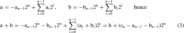
To start with the binary add operation, let two numbers a, b have the codes (a0,…,an−1), (b0,…,bn−1) and let (s0,…,sn) be the (n + 1)-bit code of their sum. We have

and

The function q is the full adder operation (1) in section 4.1 and the bits c0,..,cn are defined recursively by c0 = 0 and ci+1 = o(ai, bi, ci) for i < n. Thus, si = q(ai, bi, ci) for i < n, and sn = cn.
The algorithm to obtain the si by computing the q(ai, bi, ci) and the ci+1 = o(ai, bi, ci) is the common bit-by-bit computation of the sum, the ci being the carry bits, and corresponds to the composite circuit ADD defined in section 3.4, using full adder circuits as building blocks. Note that it is the structural type of definition that corresponds to a particular Boolean algorithm. The circuit is known as the ripple-carry adder. It suffers from a long execution time T = n*Tf due to the connection of the full adder building blocks in series, Tf being the processing time of the full adder. The circuit complexity is in O(n). The first full adder stage actually performs as a half adder and could be substituted by the simpler half adder component, but maintaining the carry input to the first adder is useful for cascading several multi-bit adders.
If one desires the result of the add operation to be encoded similarly to the operands, i.e. with n bits, too, which is usual in order to avoid the growth of the codes for every add operation, (s0,…,sn−1) is the result and the carry output cn = 1 is the overflow error condition of the result exceeding the range of the n-bit binary codes. The add operation with the n-bit result (s0,…,sn−1) irrespective of the carry is the add operation mod(2n) that computes the binary code of the remainder of the sum a + b divided by 2n. The n-bit adder with the carry input and output generalizes the full adder function by changing the inputs a, b and the output q to binary coded base 2n digits. Every n-bit add circuit with an (n + 1)-bit result performs the mod(2n) add operation and generates the overflow bit.
The carry input to the n-bit adder can also be thought of as a control input that selects between the alternative computations of a + b and a + b + 1. In fact, for n = k + m the n-bit ripple-carry adder can be regarded as the composition of a k-bit and an m-bit adder, so that the carry output of the k-bit adder selects the between the two alternative computations of the m-bit adder which is similar to executing them as the alternative branches of an ‘if’ control structure (section 1.2.2).
As the add operation may occur many times within an algorithm, a short execution time is desirable for it. There are various schemes to reduce the processing time by providing a faster carry propagation and by lowering the total depth of the adder circuit at the expense of an increased gate count. One is the carry select scheme that converts the control dependency of the m-bit add on the k-bit add into a data dependency by executing both branches in parallel and selecting using the carry bit of the k-bit adder (see section 1.4.2). Listing 4.1 lists the structural VHDL definition for a 16-bit adder architecture with k = m = 8. If n is a power of 2, the carry select scheme can be applied recursively to half size adders which raises the gate count to O(n1.6) but decreases the processing time to O(log n) (three half-size adders are needed, hence for n = 2r a total of 3r = n1.6 1-bit adders are needed). Thus, the component ADD8 would be implemented similarly with three ADD4 components etc. For other circuit schemes to achieve a faster binary add operation, see [44].
entity ADD16 is
   port (a,b: in bit_vector(15 downto 0); ci:in bit; q:out bit_vector(15 downto 0); co:out bit);
end ADD16;

architecture structural of ADD16 is
     component ADD8
         port (a,b:in bit_vector(7 downto 0); ci:in bit; q:out bit_vector(7 downto 0); co:out bit);
     end ADD8;

     component SEL port(a,b,s: in bit; q: out bit); end SEL;

     signal s0,s1: bit_vector(8 downto 0);
     signal cl: bit;

   begin

    low: ADD8 port map (a(7 downto 0), b(7 downto 0), ci, q(7 downto 0), cl);
    high0: ADD8 port map (a(15 downto 8),b(15 downto 8),‘0’,s0(7 downto 0),s0(8));
    high1: ADD8 port map (a(15 downto 8),b(15 downto 8),‘1’,s1(7 downto 0),s1(8));
    I: for n in 0 to 7 generate
              G: SEL port map (s0(n),s1(n),cl,q(n+8));
    end generate;
    GC: SEL port map (s0(8),s1(8),cl,co);

 end structural;
Listing 4.1 The carry-select adder
The operation of incrementing (i.e., the unary operation i -> i + 1) is the special case of an add operation in which the second operand is the constant number 1 which is encoded as (1,0,…,0). Like the n-nit adder, the n-bit incrementer produces an (n + 1)-bit result. The lower n output bits encode the result of the mod(2n ) increment operation, and the upper bit indicates the overflow condition of the result not being representable with n bits (this only occurs for the all ones input encoding 2n − 1 with the result of 2n with zeroes in the lower n bits; the overflow bit ‘tests’ for the all ones code).
If the ripple-carry add algorithm is used for the increment operation, the full adders all have a zero operand and can be simplified to half adders (the first of them even to an inverter). If the first half adder is maintained and the ‘1’ input to it is changed to ‘0’, the trivial operation i → i + 0 = i is performed instead. Thus the increment operation can be controlled with very little extra hardware effort. The incrementer is faster than the ripple-carry adder but still needs the ‘linear’ time n*Th, Th being the execution time of the half adder. Now the carry to the ith stage only occurs if all previous outputs are ones which can be determined using an (i−1)-input AND function. These can be computed in ‘logarithmic’ time ld(i-1)*Ta by connecting the elementary 2-input AND gates as trees, and the increment function using such fast carry inputs to all the half adders achieves an execution time in O(log n).
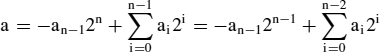
We next consider the signed binary add operation. The add operation essentially remains the same if twos-complement encoding is used instead of the straight binary encoding. Using equation (3) in section 1.1.1 the numbers a, b are related to their n-bit twos-complement codes (a0,…,an−1) and (b0,…,bn−1) through the equations
where h denotes the result of the modulo 2n add operation applied to ∑ai2i and ∑bi2i and cn is its overflow bit. The only difference is in the overflow condition if operands and the result use the same word size. For the binary encoding, the final carry output cn signals the overflow. The sum of two signed n-bit numbers is a signed (n + 1)-bit number s, the sign bit sn of which is the sign of the result. The overflow in the twos-complement case is indicated by the sign sn of the result being unequal to sn−1. By (3) the computation of sn requires an extra XOR operation:
![]()
it follows that
The signed binary increment operation with an n-bit result is the same as the unsigned or the mod(2n) one. It overflows for the maximum positive input code of (1, 1,…,1, 0) and then outputs the most negative code of (0, 0,…,0, 1).
Concerning the subtract operations for unsigned, signed and modulo 2n binary numbers, we first remark that for a mod(2n) binary number x,/x + 1 is the mod(2n) additive inverse −x of x (/x denotes the complement of x). The negation overflows for the all zeroes code only and hence can be used to test for it. The binary subtract operation mod(2n) is obtained from the equation
Adding the ‘1’ does not require an extra increment circuit but is achieved by placing a ‘1’ at the carry input of the first adder stage of the mod(2n) adder. By selecting between b and /b the same n-bit adder can be used both for the add and subtract operations which is useful to build multi function compute circuits, in particular arithmetic units for programmable processors (see Figure 1.6).
For unsigned binary numbers a, b the difference a − b is defined for b ≤ a only and then equal to the result of the binary mod(2n) subtract operation. This condition is signaled by the mod(2n) adder used to compute (6) through a ‘1’ at the carry output. The signed binary subtract operation also coincides with the mod(2n) subtract operation for the lower n bits of the result as the signed binary code of a number coincides with the unsigned code of its remainder mod(2n), and taking remainders is compatible with the add and subtract operations. The full result can be represented as a (n + 1)-bit signed binary number that is obtained by applying equation (6) to a and b sign extended to n + 1 bits. This time the overflow condition is sn ≠ sn−1 again.
A special case of the subtract operations is the decrement operation, i.e. subtracting the constant 1. As for the increment operation, the subtract circuit can be simplified and sped up to logarithmic time.
If x is an n-bit signed binary number and x ≠ −2n−1, then so is −x, and −x = /x + 1. The negation overflows for x = −2n−1 (=100..00), the most negative representable number, only as −x = 2n−1 cannot be represented as a signed n-bit number but needs n + 1 bits. Again, the overflow condition is sn ≠ sn−1 and can be used to check for this special code.
The add, subtract, negate and compare operations for signed or unsigned binary numbers x are identical to those for fixed point operations on the fixed-point numbers x/2r, for which hence the same algorithms can be used.
Related to the unsigned and signed fixed point subtract operations are the compare operations ‘a ≤ b’ and ‘a = b’ viewed as a Boolean functions. ‘a ≤ b’ for unsigned n-bit operands is equal to the carry output from the subtract operation b − a and hence computed by any subtract or combined add and subtract circuit if the value of 1 is interpreted as ‘true’. The comparison of signed numbers requires computing the sign of b − a instead of the carry. ‘a = b’ can be evaluated by comparing bit per bit and computing the conjunction of all bit comparisons with an AND gate tree as the codes are equal if and only if the represented numbers are equal, or be reduced to the signed or unsigned ‘≤’ operations or to a test for zero using the equivalences
![]()
Testing for the special values 0, −1, −2n−1 and 2n−1 − 1 is equivalent to testing for the overflow conditions of the increment and negate operations.
4.3 ADD AND SUBTRACT FOR REDUNDANT CODES
A still more effective way to speed up the add operation is obtained by using a redundant encoding for the numbers. We first consider the code using the 2n-tuple (u0,…,un−1, v0,…,vn−1) for the number

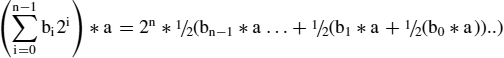
Every binary number (m0,…,mn) can be converted into a ‘double’ code by appending (0,…,0), and every double code can be reconverted to a binary one by performing the binary add operation according to equation (7). For two redundant codes a, b encoding numbers a′, b′, the conditions a = b and a′ = b′ are no longer equivalent.
If u and v are the binary numbers (u0,…,un−1) and (v0,…,vn−1), then the redundant code (u0,…,un−1, v0,…,vn−1) encoding their sum is obtained without any computational effort. An encoded add operation using a redundant code for the first argument and the result and a binary code for the second argument is any function B2n × Bn → B2n+2 mapping a double code (u0,…,un−1,v0,…,vn−1) of a number a and the binary code (b0,…,bn−1) of a number b to a double code (s0,…,sn,t0,…,tn) of the number a + b. Encoded add operations are not uniquely defined as the double codes for the result are not unique. A possible choice is
![]()
where q, o are the full adder outputs. This follows from equation (1) in section 4.1; the multiplication by 2 is realized by the t word being shifted by one bit position. The computation of the result code can thus be performed by n full adder circuits in parallel in the time Tf irrespective of n. From this add operation one derives an encoded add operation
![]()
accepting double codes for both operands that also operates in the constant time 2*Tf, namely by adding the halves of the second operand one by one.
These add operations can now be composed. If k redundant codes have to be added up to a single redundant result code, one can arrange them as a tree to obtain the time of 2*Tf*ld(k) for the total computation. The only disadvantage of the redundant add operation is the redundant encoding of the result which usually needs to be converted (added up) to a binary code. If, however, a set of k binary numbers have to be added up, only the final result would have to be converted.
The redundant encoding defined by equation (7) and the fast add operation generalize to codes (u0,…,un−1,v0,…,vn−1) where the ui are base-k digits and only the vi are binary digits. Listing 4.2 shows a 16-bit adder using this redundant kind of code for the first operand and the result and the non-redundant binary code for the second operand. Four 4-bit sections serve as base-16 adders.
entity XADD16 is
       port ( a,b:in bit_vector(15 downto 0); xa: in bit_vector(3 downto 0);
                 q:out bit_vector(15 downto 0); xq: out bit_vector(4 downto 1)
                   )
end XADD16;

architecture struct of XADD16 is
          component ADD4
	        port (a,b: in bit_vector(3 downto 0); ci: in bit; q: out bit_vector(3 downto 0); co: out bit)
          end ADD4;
begin
     g0: ADD4 port map(a(3 downto 0),b(3 downto 0),xa(0),q(3 downto 0),xq(1));
     g1: ADD4 port map(a(7 downto 4),b(7 downto 4),xa(1),q(7 downto 4),xq(2));
     g2: ADD4 port map(a(11 downto 8),b(11 downto 8),xa(2),q(11 downto 8),xq(3));
     g3: ADD4 port map(a(15 downto 12),b(15 downto 12),xa(3),q(15 downto 12),xq(4));
end struct;
Listing 4.2 Redundant adder built from 4-bit sections
The signed digit encoding of a number m by the tuple (m0,…,mn−1) so that

where the digits mi take the values − 1, 0, 1 and hence also need at least two bits each for their encoding also yields a fast add operation by using the redundancy in such a way that the carry does not propagate by more than one place. The negate operation on the signed digit code is by negating the digits individually in parallel. It is hence easy to convert a signed binary number into this representation, and the reconversion to a signed binary code is by splitting m into a difference of two positive binary numbers and performing the binary subtract operation.
A fast algorithm to compute a sum code (s0,…,sn)of two signed digit codes (u0,…,un−1) and (v0,…,vn−1) is as follows. For every i ≤ n − 1 one computes the conditions:
![]()
the carry digit
![]()
Finally, sn = cn−1. Thus si only depends on ui, vi, ui−1, vi−1, ui−2, vi−2, and all can be computed in parallel (this also holds for the redundant add operation presented first). The fact that si does not depend on the lower bit positions is called the ‘on-line property’ in the literature [6]. It implies that they do not even need to be known at the time si is computed and that their computation may be pipelined with the computation of si.
4.4 BINARY MULTIPLICATION
The product of two numbers

is the (n + m)-bit number
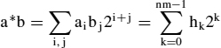
Thus the n*m single bit products ai bj have to be computed and the results for a given bit position i + j have to be added up by means of single bit adders passing carries as needed. This can be done in various ways, using as its building blocks full adders extended by an AND gate (the single-bit multiplier) to form the product aibj. They are depicted in Figure 4.1 for the case of n = m = 5 by circles that output the higher (carry) bit to the left or straight down and the lower (sum) bit down on the diagonals to the right, and receive up to three inputs, a product aibj, and the others from other building blocks. The jth row receives the inputs an−1bj,…,a0bj, and the output bits h0…h2n−1 appear at the right and lower sides of the diagrams. A circle that only receives the product input Just passes it, and if there is only one additional input the circle acts as a half adder. The version in Figure 4.1a corresponds to adding shifted versions of a with n ripple-carry adders operating in parallel and has the disadvantage of a fairly long processing time of (3n − 2)* T, T being the processing time of the full adder (the products are computed by the AND gates in parallel and only add a single AND gate delay which is neglected). The version shown in Figure 4.1b uses the same number of building blocks but a different carry routing for the nodes above the diagonal and multiplies in a time of (2n − 2)*T (the 1st row just passes the product inputs to the 2nd). The computation of the less significant half word of the result only takes (n − 1) *T. For a multiplier modulo 2n that only computes the less significant word only the adders on and above the diagonal are needed.

Figure 4.1 Multiplier networks with different carry propagation schemes
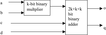
Figure 4.2 Extended k-bit adder component
The third propagation scheme in Figure 4.1c ends up with a redundant code for the upper half word of the result, i.e. two n-bit binary numbers that still need to be added up to the most significant word of the result, using e.g. a carry select adder. It takes the time of (n − 1)*T plus the carry select adder time and can be thought of as cascading n − 1 adders, each adding a redundant code and a row of products.
A still faster multiplier operating in logarithmic time can be obtained by using a tree of redundant adders instead of cascading them, the so-called Wallace tree [44], and adding up the upper word parts with a carry select adder or some other adder also operating in logarithmic time. For all of these schemes, the input data must be held unchanged throughout the processing time as they are used in all adder rows.
The multiplier networks in Figure 4.1 are regular structures constructed from a single type of component, the extended full adder including the AND multiplier. It adds the multiplier result and two more bits and output a 2-bit result. Current FPGA chips provide this function in a single cell. The extended adder component generalizes to the k-bit extended adder that is defined as a combined k-bit multiply and add circuit that forms the product of two k-bit numbers and adds it to two more k-bit inputs to arrive at a 2k-bit result (Figure 4.2). For n = m*k, the same network structures as in Figure 4.1 implement n-bit multipliers with m*m extended k-bit adder components. The extended k-bit adder (or add-subtract circuit) can also be used as a component to implement n-bit add (add/subtract) functions and could be used as a cell in a coarse-grained FPGA architecture.
The product of a twos-complement signed number a by an unsigned or signed number is formed according to the representations
and differs from the unsigned product in the most significant word only. If ‘∗s’ denotes the Boolean function computing the product of signed binary numbers, and ‘∗u’ the unsigned version explained before then
where the products by an−1 and bn−1 just make the subtract operations of b or a conditional on them, and the product by 2n means that the subtract operations are from the upper half word. The same multiplier structures can be used and extended to conditionally subtract from the most significant word, or to perform a subtract in the last row containing the products aibn−1instead of adding and the signed versions of the add and shift operations (the leftmost carry is replaced by the sign).
If one of the operands, say b, is a constant, the multiplier circuit can be simplified significantly. In fact, all aibj can be evaluated to ai or 0 depending on bj. Thereby all AND gates are eliminated, and one has to add up selected shifted versions of a, namely the versions 2j*a for those j satisfying bj = 1. In the special case of just one of the bj being 1 no add operation needs to be performed at all, and the output is the shifted word 2j*a. Obviously, the structure of the circuit now depends on the constant operand.
All of the above binary multiplier circuits for two variable n-bit operands use n2 full adder building blocks to add up the products and have a gate count in O(n2). A reduction of this complexity can be achieved by applying the formula
that reduces a (2r)-bit product to three r-bit products. The recursive application reduces the complexity to within O(n1.6) if ripple carry adders are used, and to O(n1.6 log(n)) with carry select adders. With the fast adders the processing time adds up to O(log(n)2) using the fact that the three products in the formula can be computed in parallel. If log(n) multipliers can be used in parallel, the execution time per multiply becomes O(log(n)) as for the Wallace tree but the gate count raises to O(n1.6log(n)2) only. The Wallace tree uses its gates more efficiently but needs too many steps to perform the multiplication. The multiplication based on equation (10) pays off and is used for large bit sizes (>64) only. The complexity of multiplication algorithms can be as low as O(n log(n) log(log((n))) [54], by interpreting the multiplication as a convolution for which a fast algorithm exists (cf. section 8.2.3).
For the computation of the product an online property can be achieved if redundant codes are used for the adder implementation (at least for the upper half of the result word). It is by applying still another scheme to connect the adders given by the recursion
![]()
where Aj, Bj denote the binary numbers presented by (an−j,..,an−1) and (bn−j,..,bn−1) so that a = An, b = Bn. Adding Bj and 2Aj−1 may still cause a change in the bit position j of the 2j-bit result, but can be arranged not to do so in the higher ones, i.e. the upper j − 1 bits can be computed from the upper j bits of the operands [6]. This online property is useful in fixed point computations with a fixed number of places where instead of the full product a rounded version of the most significant part is needed.
4.5 SEQUENTIAL ADDERS, MULTIPLIERS AND MULTIPLY-ADD STRUCTURES
In this section we derive implementations of some of the add and multiply algorithms discussed before that serially reuse components for the sake of efficiency and provide cost-effective register arrangements to store the intermediate results and select them for later operations.

Figure 4.3 Serial adder
If h is the depth of the add or the multiply circuit, its processing time is h*T. As pointed out in section 1.5, if the multiplier is used at its maximum rate corresponding to its processing time, then the adder circuits performing the computation are used with an efficiency of 1/h only. Pipelining can also be used to raise the efficiency. The layered structure of the multiplier in Figure 4.1(c) can be used to pipeline its operation by inserting registers between the layers both for the intermediate results and for the operands. Then the multiplication still takes the same time (even a little more due to the registers) but subsequent multiplications can be started at the rate given by T that is independent of h, and the efficiency becomes close to 100% (with a proportional increase of the power consumption). The storage and power requirements become lower if the layers are grouped into sets of h′ layers and the ndnpipelining is implemented for these only. Then the pipelined multiplications can be started at a rate of h′*T and the efficiency raises to close to 1/h′.
The n-bit binary ripple-carry adder applies n identical full adder circuits at all bit positions. The full adders are connected in series via the carries. The full adder operations can be executed serially on a single full adder circuit, starting with bit 0, by using as the full adder inputs for the ith or i-th application the bits ai, bi from the operands and the carry signal ci that has been computed as the overflow oi−1 in the previous application. oi−1 must be stored in a flip-flop in order to be able to use it in the subsequent step, but it is no longer used thereafter and the same flip-flop can be used to store all the carries in sequence (Figure 4.3). It must be cleared to zero at the start of the serial computation. This also eliminates the need to select the carry input from different sources during the sequence of steps.
The simplicity of the serial adder circuit depends on the input bit pattern being applied serially to the same sites and on also producing the output pattern this way. Conversely, the inputs and outputs to the previous ‘parallel’ adder circuits were supposed to be applied in parallel. Auxiliary circuits are needed if the inputs to the adders are applied differently. A selection circuit for the input bits for the serial adder is needed if these are applied in parallel on n signal lines, using n-1 select gates connected as a tree as in Figure 1.3 for each of the two input words. The processing time of these select trees is proportional to their depth ld(n) and drives up the processing time of the serial adder, and also requires the generation of a select address. The extra processing time and the need for a select address are eliminated by receiving the input bits from two n-bit shift registers using the same clock signal as for the carry flip-flop (increasing the power consumption). This maximum clock is given by the processing time of the half adder plus the set-up and hold time for the flip-flop. As the shift registers needs to be loaded in parallel from the input lines, they also include n − 1 select gates each, but this time the select operation is pipelined with the full adder operation and does not contribute to the processing time. Even not counting the input register flip-flops which probably would also be used for the inputs to a parallel adder, one concludes that a need to select from the parallel input bits drives up the hardware costs to similar costs as for the parallel adder. If the output bits from the serial adder are needed in parallel, another shift register can be used, again eliminating the need to select storage locations for the individual bits. One of the input shift registers can be used for this purpose (Figure 4.4), too. This figure does not show the signal selecting parallel input and a handshaking signal indicating n clock edges later that the result is ready. Their generation still requires an extra effort not needed for the parallel adder.

Figure 4.4 Serial adder with parallel input and output

Figure 4.5 Serial multiplier using the Horner scheme
As the n by n bit binary multiplier is also built up from n2 identical full adder plus AND gate components, all their operations could be executed in sequence, this time requiring n bits of intermediate storage. More generally, the n-bit multiply operation broken up into m2 identical k-bit extended add operations that can be serialized.
The n by n bit multiplier in Figure 4.1(a) can also be represented as a cascade of n rows that are parallel adders and can be realized by using the same parallel adder in n sequential steps. It needs a single n-bit register to pass a partial sum to the next step (Figure 4.5) which avoids the overhead for selecting input bits. The first operand a is input in parallel to the adder while the bits of the second operand need to be input serially (e.g. using a shift register). The output bits come out serially of the least significant output bit of the adder according to the serial execution of the Horner scheme (where multiplying by ½ is equivalent to shifting down):
and may be moved into a shift register. After n steps, the register holds the most significant half of the result. Again, there is some extra effort for serializing b and for generating signals indicating the start and the end of the multiply operation, but this time the overall hardware costs are in O(n) and thus significantly less than for the ‘parallel’ multiplier circuits. The signed multiply is implemented by changing the cycle adding bn−1*a to a subtract cycle and by using a signed adder circuit. The circuit in Figure 4.5 generalizes to serially adding up k*n bit products using extended k-bit adders.
Instead of multiplying via the AND gates, the multiplication step can also be realized by selecting between the adder output and directly passing the shifted input. This amounts to skipping the add operation and can be exploited to speed up the sequential multiplication in the case of the second operand containing many zeroes. Moreover, if the second operand contains a sequence of ones from bit positions k to l, then the sum of the corresponding powers 2r∗a is equal to 2k+1∗a − 2r∗a and can hence be computed with two add steps and some shifts (Booth's algorithm). The processing time for the multiplication becomes data dependent which is considered as a disadvantage in some applications.
The row of two output extended full adders from Figure 4.1(c) can be also be used in n sequential steps. It requires two n-bit registers and requires their contents to be summed up in a final step. The second register is for the carry words and gives this multiplier structure the name of a carry-save multiplier. The sequential steps can be performed at nearly the maximum rate of the individual extended full adder component. The carry-save multiplier performs in linear time and with a linear hardware effort. The adder components are used at close to 100% efficiency as in the case of the fully pipelined parallel multiplier. The carry-save multiplier is much faster than the structure in Figure 4.5 even if a fast adder is used there and if the final add to convert from the redundant code is performed serially. In comparison to the parallel circuit using n2 adders, it cannot exploit the adder tree structure or be pipelined.
Adding bi*a to the right shifted output word in the serial multiplier of Figure 4.5 is easier to implement but equivalent to adding a left shifted version of it to the unshifted 2n-bit output register. If it is implemented this way, then at the start of the multiplication the register need to be reset to zero. If not, the product is actually added to its previous contents. Thus at no extra hardware costs, this serial multiplier performs a multiply-and-add operation. The shifted output register version can be modified to perform it, too, and a variant of it is shown in Figure 4.6 using the carry-save multiplier scheme.
The upper part containing the AND multipliers, the full adders and the three registers C, L, H is the carry-save multiplier circuit outlined above, the C register holding the carry word. After the last cycle of a multiply operation the redundant code of the high word of the result would stand in the registers C and H while the L would hold the low word of the result. The remaining registers serve to implement the multiply-add function. After the last cycle the next multiply operands a, b are applied, the redundant code of the high word is moved into the registers c, h instead, the low word is loaded into H, and C is cleared. The new multiplication then continues to add to H while at the same time the high word of the previous result is added up bit by bit in the serial adder consisting of the full adder and the D flip-flop and applied to the carry-save adder through the upper bit of the H register. The individual product then takes n cycles, and the add operation to convert from the redundant code is pipelined with the next multiplication. It is at the end of k multiplications only that a single redundant code remains to be added up to a binary one. A serial counter-circuit can be used to include a third result word accumulating the overflows occurring in a series of multiply-add operations.

Figure 4.6 Serial carry-save multiplier-accumulator (MAC)
4.6 DISTRIBUTED ARITHMETIC
Sums of products
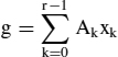
with constant coefficients Ak, i.e. considered as functions of the xk only, can be evaluated for small n quite efficiently using look-up tables, yet not using the entire multi-bit binary or fixed point codes of the xk to address the table, but individual bit xk,i for the same arbitrary bit position i. Then fairly small look-up tables addressed by r bits suffice. For n = 3..6 such are offered by the cells of current FPGA chips. Therefore this approach yields an efficient implementation for multiple multiply-and-add operations on such chips. For all k,
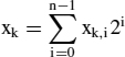
hence

with
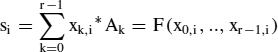
F is the function of r Boolean inputs defined by F(b0,…,br−1) = ∑k bk*Ak. It outputs n′-bit words with n′ > n due to the multiple add function and is realized using a table. Then, g is summed up serially using the Horner scheme using the sequential structure in Figure 4.7 which is similar to Figure 4.5:

Figure 4.7 Serial computation of a dot product using distributed arithmetic

The operand bit xk,i need to be input serially using e.g. shift registers clocked synchronously with the add and shift steps.
For every bit of the result of F, a look-up table from a separate FPGA cell is used. Thus the required memory is taken from the FPGA configuration resources. This also allows an easy change of coefficients without having to redesign the circuit structure and its mapping. The number r of products is limited by the size of the available look-up tables. Longer input sequences can, however, be handled by breaking the g sum into small parts and summing up the outputs of the corresponding tables, or by combining several cells to obtain larger look-up tables. It is not possible, however, to reuse the same length r hardware circuit for the different sub-sequences as the coefficients in the LUTs cannot be changed easily as this amounts to reconfiguration which takes some time if it is supported at all (only some Xilinx FPGA families can serially load a LUT from an application circuit). If, however, the same sum-of-products operation has to be applied to a block of vectors, the swapping of the LUTs can be performed once per block only and may become affordable. The hardware effort in using the circuit in Figure 4.7 is considerably less than using r serial multipliers in parallel and adding up their results, and the speed is faster.
A trick to cut the required memory by a factor of two (cf. [3]) is to represent the signed xk inputs in the form:

and to replace F by:
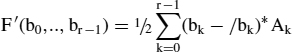
Then:

F′ satisfies:
![]()
The table for F′ only needs to provide the entries for x0 = 0. x0 is only used to complement the other bits and to change the add to a subtract operation using an add/subtract circuit instead of the adder.
4.7 DIVISION AND SQUARE ROOT
The division of an unsigned 2n-bit number a by an n-bit number b such that a < 2nb is computed in a sequence of operations conditionally subtracting products 2kb from a as long as the result is positive, for k decreasing from n-1 to 0. The sum over those powers 2k for which the subtraction was carried out is the result of the division. The condition of an intermediate difference a′ satisfying a′ ≥ 2kb corresponds to the carry bit being set after performing the binary subtract operation. Thus the divide step can be realized by using a binary subtract circuit and a selector between a and a − 2kb controlled by the carry bit, and outputting the carry bit to the kth bit position of the result. Due to the serial composition of the operations, a serial execution on the same conditional subtract circuit can be nearly as fast. The carry outputs during the time steps can be shifted into a result register. After performing the algorithm the remainder of the division is obtained as the result of the subtract operations. Equivalently to subsequently subtracting 2kb from an intermediate difference a′ one can subtract 2nb from 2n−ka′. This corresponds to shifting a′ to the left instead of shifting b to the right.
The conditional subtract operation can also be realized with an add/subtract circuit controlled by a function select input again. If the subtract operation a′ − 2kb sets the carry, then in the next step a′ − 2kb will be changed by subtracting 2k−1b, otherwise by adding it as a − 2k−1b = a − 2kb + 2k−1b. A common circuit for the sequential computation in shown in Figure 4.8, again shifting a to the left instead of b to the right. a is first loaded into the shift register L, the carry flip-flop C is set, and H is cleared. Then a first subtract is performed inputting from the lower n− 1 bit of H and the highest bit of L and storing the result in H, and shifting L to the left using the carry as input into the lowest bit of L (L is used for the result bits as well). After a total of n add/subtract and shift operations the result of the division stands in L. A final conditional add operation is required to obtain the remainder of the division in H. As in the circuits discussed before, the circuit starting and generating the clock sequence is not shown, only the data registers and the add/subtract circuit (the so-called data path).
The same principle of performing a binary search for a maximum solution x of an equation f(x) ≤ a (f being a monotonic function, f(x) = b*x for the division) can also be applied to calculating the square root of a number a (here, f(x) = x*x). One adds decreasing powers 2k starting with k = n/2 − 1 as long as the square of the sum is less than a, keeping track of the difference d of a and the square of the sum s. In every add step d decreases by 2k+1 s + 22k (or, 2−1−kd decreases by s + 2k−1) which can be realized with conditional subtract operations again.

Figure 4.8 Binary n-bit serial divide circuit
For the square root of fixed point numbers a with 0.25 <= a < 1, another common procedure is the approximation using the iteration bi+1 = ½ (bi + a/bi) and starting from b0 = 1 which converges quadratically but requires division.
4.8 FLOATING POINT OPERATIONS AND FUNCTIONS
Floating point operations are a lot more complex than fixed point ones, especially for the high precision types. There are, however, algorithmically derived from fixed point operations, and thus covered by the preceding sections. Special design tricks can be found in [44]. A common optimization in digital computations is to substitute floating point computations by fixed point ones after an analysis of the required precision. If the required frequency of floating point operations is low enough, they become a candidate for serial execution on a single or on a few processors and even for software implementations, i.e. for synthesizing them from fixed point operations executed on simple programmable processors.
The product of two normalized floating point numbers r1 = m12s and r2 = m22t with 1 ≤ m1m2 < 2 is r1*r2 = m1*m2 2s+t. The following operations have to be performed:
- Extract exponents and form e = s + t.
- Extract mantissas and form the fixed point product m = m1*m2.
- If m ≥ 2 then normalize m, increment e.
- Round m.
- Extract signs and derive sign of result.
- Pack the bit fields.
Of these, the multiply operation is the most demanding one. It is a fixed point operation only requiring the most significant part of the product to be computed.
If s ≤ t, the sum is derived from the formula r1 + r2 = (m1*2s−t + m2)2t and requires the following operations:
- Extract exponents, order according to s ≤ t.
- Denormalize m1 (multiply by 2s−t).
- Fixed point add/subtract operation according to sign bits to get m = (m1*2s−t±m2).
- Normalize and round m and correct exponent accordingly.
- pack the bit fields.
m may be small due to bit extinctions, and the normalization step requires a multi-bit shift depending on the number of sign bits. Extinction introduces an error that cannot be read off from the code.
While binary and signed binary adder and multiplier building blocks can be composed to yield add and multiply operations on words of arbitrary sizes, the floating point operations are not easily extended to higher precision operations. According to [54], the true sum of the rational numbers exactly represented by two floating point codes a, b with |a| ≥ |b| can be represented as
![]()
where ⊕, ![]() denote the (rounded) floating point add and subtract operations. The rounding error of the floating point add operation corresponding to the places of b lost during the denormalization step can thus be computed in terms of floating point operations only (although not efficiently). Such a double word representation of a number as a sum of two floating point numbers can also be obtained for the true product of two numbers, using an operation that divides a floating point code into a sum of two half mantissa size codes for which the floating point product is exact (or one clearing the lower half of the mantissa). The operations to compute the rounding errors as floating point codes are useful floating point building blocks that can be generated as by-products of the implementations of the rounded floating point operations quite easily, but are not available on standard processors. Using them, full double precision operations can be derived from single precision ones, and the accumulation of rounding errors can be tracked to some degree.
denote the (rounded) floating point add and subtract operations. The rounding error of the floating point add operation corresponding to the places of b lost during the denormalization step can thus be computed in terms of floating point operations only (although not efficiently). Such a double word representation of a number as a sum of two floating point numbers can also be obtained for the true product of two numbers, using an operation that divides a floating point code into a sum of two half mantissa size codes for which the floating point product is exact (or one clearing the lower half of the mantissa). The operations to compute the rounding errors as floating point codes are useful floating point building blocks that can be generated as by-products of the implementations of the rounded floating point operations quite easily, but are not available on standard processors. Using them, full double precision operations can be derived from single precision ones, and the accumulation of rounding errors can be tracked to some degree.
For the non-normalized floating point format proposed in section 1.1.1 a simple heuristic to keep track of the precision is to form products to the minimum number of places of the operands. For the logarithmic encoding, fairly efficient add and multiply operations have been derived [82].
The square root and reciprocal functions are evaluated using the algorithms in section 4.6 or iterative procedures starting from low precision approximations taken from a ROM table. The standard transcendental functions are all evaluated from polynomial or rational approximations on certain intervals and extended from there by means of functional equations [47]. The sine function e.g. is approximated on [0, π/2] and extended using its symmetry and periodicity. Higher precision floating point formats require higher order polynomials, the allowed approximation error being of the order of magnitude of the least significant bits of the mantissa. For the sine and exponential functions there are special CORDIC algorithms exploiting their special properties that compute their results by means of the fixed point add, subtract, compare and shift operations only that are most suitable for FPGA [46, 82] (cf. exercise 8).
For the evaluation of polynomials p(x) the Horner scheme is attractive as it eliminates multiplications and the storage of powers of x:

It combines the multiply and add operations in a different way from the MAC structure in section 4.5, namely by multiplying to an intermediate result and then adding instead of adding to the intermediate result, and must be supported by a different circuit structure. The coefficients are constant and may be supposed to be scaled so that for arguments x ∊ [−1,1] the result may be represented in a given fixed point format on [−1, 1]. After every multiplication rounding is supposed to be applied so that all intermediate results can be represented in the same format. A circuit realizing this composite operation would be a useful building block for realizing functions through polynomial approximations. For rational approximations, other primitives, e.g. the expressions (a + 1/x) or (ax + b)/(cx + d) can be considered.
In some applications, it is sufficient to provide ROM function tables for selected arguments of certain functions only. Starting from a table, the values at intermediate arguments may be derived by some low-order polynomial interpolation to a desired precision.
4.9 POLYNOMIAL ARITHMETIC
For a primitive binary polynomial p(x) = ∑,piXi of degree n the multiplication of polynomials mod(p) is the composite operation of taking the remainder of the product polynomial after its division by p. The powers Xk mod(p) of the polynomial X exhaust the m = 2n − 1 non-zero polynomials of degree < n and can be used to encode the numbers k with 0 ≤ k < m by their coefficients, as proposed in section 1.1.1. For larger k, the remainders of the Xk repeat mod(m) (Xm = 1 mod(p)).
For this encoding, the increment operation is particularly simple. If

The tuple representing the number k is thus shifted and XOR'ed by the shifted-out bit gn−1 at the positions of the non-zero coefficients of p. This is the operation of a shift register with XOR feedback from the output shown in Figure 4.9. The remainder of Xm−1 increments to the polynomial 1, and the increment operation repeats after m steps. If the number of non-zero coefficients of p is small, the feedback shift register is less complex than e.g. a synchronous binary counter. Apart from the simplicity of these feedback circuits, shift register sequences generated in this way also have interesting statistical properties and can be used to generate pseudo-random numbers [83].
The general add operation is more complex, however. It is the product Xr∗Xs = Xr+s that corresponds to the add operation modulo m of the exponents. Let Xr and Xs be the polynomials


Figure 4.9 mod(7) counter automaton based using the polynomial 1 + X + X3

Figure 4.10 Polynomial multiplication ( * : AND, + : XOR )

Figure 4.11 Computing the remainder of the polynomial q divided by p(X) = 1 + X + X3
Thus (g0,…,gn−1) and (h0,…,hn−1) are the codes of r, s. The product polynomial is given by

The add operation in the field B is the XOR operation. The Xk with k ≥ n must be substituted by their remainders modulo p which depend on p. If the polynomial p(X) = 1 + X + Xn is used (for some n it is primitive), then Xk = Xk−n + Xk−n+1 mod(p). The total number of XOR operations to compute the code of r + s from the codes of r and s is then n2 − 1 that can be arranged so that the processing time is logarithmic. An application would be to compute relative addresses in the case that subsequent address codes to read out a memory are generated by a shift register implementing the above increment operation (see section 5.1.3).
Multiplications of binary polynomials and remainder computations can be carried out serially using shift registers. The coefficients gk are applied to an n − 1 bit shift register in reverse order (starting with gn−1 at the input and all flip-flops reset to 0). Every shift operation moves the coefficients to the left so that gk+i appears at the output of the ith stage. After n − 1 clocks, g0 is applied to the input, and g1…gn−1 stand in the register. Thereafter, zeroes are applied to the input. The shift register taps are multiplied by the coefficients hn−1, hn−2,…to generate the coefficients qk+n−1 = ∑hn−1−igk+i of the product g*h in reverse order, starting from q2n−2 (Figure 4.10). These are fed into a second shift register with feedback from the output according to the primitive polynomial p to perform the substitution of Xn appearing at the register output by its remainder (Figure 4.11). After 2n − 2 shift clocks, the result code stands at the inputs of the flip-flops of the second register.
4.10 SUMMARY
The Boolean functions realizing arithmetic operations on number codes have been found to have moderately complex algorithms. Binary arithmetic could be mostly constructed from full adder components and their generalizations, the mod(2n) adders. With some hardware effort, faster add circuits could be obtained. While parallel multiply circuits do not use the gates efficiently, serial multipliers reusing a single mod(2n) adder were found to use it quite efficiently. Other serial circuits were demonstrated for computing sums of products and for division.
EXERCISES
- Formally verify that the algorithms given for the n-bit unsigned and signed binary add and subtract operations with an (n + 1)-bit result are correct.
- Write out the behavioral and structural VHDL definitions of an n-bit adder with a carry input and an overflow output.
- Give a structural VHDL definition for a fast 16-bit incrementer using multiple AND gates to compute the carry bits.
- Verify the signed digit add algorithm in section 4.3, give a structural VHDL definition for a generic n-digit adder, and determine its gate count as a function of n.
- Work out a 16-bit serial MAC as in Figure 4.6 accumulating 1024 products with an additional 10-bit overflow word into a VHDL entity. The 16-bit operands will be read from external memories. Extend to signed multiply-add operations.
- Design a combined multiply-and-add circuit for the evaluation of polynomials similar to the structure in Figure 4.6. After the n carry-save cycles the result of the multiplication by x is added bit by bit to the coefficient and immediately applied as the b operand to the next multiply.
- Implement a 4-bit extended adder component with handshaking signals as a VHDL entity and use it as a component in an n-bit multiplier circuit.
- For a number p with 2n−1 < p ≤ 2n the remainders mod(p) can be represented as binary n-bit numbers. Design a serial mod(p) multiplier that computes the product of two remainders in n cycles. Show how this multiply operation can be derived from the binary n-bit multiply operation with a 2n-bit result in the special case of p = 2n − 1.
- A CORDIC algorithm to compute the trigonometric functions of some n-bit fixed-point input x ∊ [0, 1] starts by initializing a 2 × 2 matrix A to the unit matrix and subsequently multiplying matrices
 to it (slightly scaled rotations by αi = atan (2−i) if xi ≥ αi, where the sequence (xi) is defined by x0 = x, xi+1 = xi − αi if xi ≥ αi, xi+1 = xi otherwise. After n steps, A is close to a scaled rotation by x, and sin(x), cos(x) and tan(x) are easily derived from it. The matrix multiplications only involve shift and add operations. Derive a serial data path performing the described operations.