
2
Hardware Elements
2.1 TRANSISTORS, GATES AND FLIP-FLOPS
2.1.1 Implementing Gates with Switches
Elementary building blocks implementing the Boolean operations AND, OR, NOT or SEL from which all Boolean functions can in turn be constructed (see section 1.3.1) are realized quite easily by electronic means. A simple solution that was actually applied in the early days of computing is the use of electrically controlled, mechanical switches. The single basic component is the controlled switch with a control input G, a coil connected between G and a ground reference C, and the poles S, B, M of the mechanical switch (Figure 2.1). If a sufficiently high voltage is applied to G w. r. t. C, the magnetic force of the coil breaks the connection from S to B and makes the one from S to M, and hence performs a selection between the voltage levels applied to B and M, depending on the control input. An interval of voltage levels that cause the switch to be actuated is used to present the Boolean 1 while the voltages near zero represent the 0, all voltages being referenced to C. This SEL building block fulfills the requirement that the input and output signals be compatible. It can thus be composed with others. The high voltage level can be selected from a power supply (denoted ‘+’ in Figure 2.1). To output a zero voltage to another coil, the corresponding select switch input can be left open, as the unconnected coil will assume the zero level by itself. Thus, the switch can be simplified to a break or a make switch actuated by the field of the coil. A break switch connected to ‘+’ realizes the NOT operation.
The parallel and serial compositions of make switches shown in Figure 2.1 implement the OR and AND functions. In the serial composition the switches controlled by X and Y must both close to output the ‘+’ level. The parallel and serial compositions generalize to networks of switches with two dedicated nodes. The network is in the state f(a1,…,an) depending on the state ai of the switches it is composed of, the possible states being 1 (‘closed’) and 0 (‘open’). If a second network of switches is in the state g(b1,…,bm), then their serial and parallel compositions are switch networks with two dedicated nodes with the state functions AND(f(a1,…,an), g(b1,…,bm)) and OR(f(a1,…,an), g(b1,…,bm)).
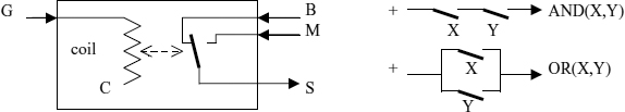
Figure 2.1 Switch-based SEL building block, and AND and OR switch circuits

Figure 2.2 N-channel transistor switch and equivalent circuit
Unfortunately electromechanical switches are slow, consume much space and power and suffer from a limited lifetime. Modern electronic computers use networks of transistors instead which behave like electronic switches and are used in a similar fashion to the electromechanical switches, but are cheap and fast solid state devices with a low power consumption and almost unlimited life that, moreover, have microscopic dimensions and can be integrated in their thousands into silicon chips. For an overview of the various classes of transistors and circuits implementing the gate functions, we refer to [2] and concentrate on the NMOS technology and on the most important and elegant one, the CMOS technology invented as long ago as 1963.
The common CMOS (complementary metal oxide semiconductor) technology uses two kinds of insulated gate field effect transistors, the n-channel and the p-channel devices. The transistor symbols in the figures are denoted accordingly. These transistors have three terminals, the source and drain terminals (S, D) and the gate (G) which is the control input (for the sake of simplicity, the influence of the potential of the silicon substrate beneath the gate is ignored). For the n-channel transistor (Figure 2.2) with the source S near the ground reference (the negative supply), the gate input G at the H level causes a low resistance connection from S to the drain D whereas an L level disconnects S and D. The device is voltage controlled; no current flows into the gate once the tiny input capacitance Cin has been charged, as shown in the simplified equivalent circuit in Figure 2.2. The transistor, switch is modeled as an ideal switch put in series with a resistor, which is valid for small output voltages only. For the complementary p-channel transistor, the S terminal is at the level of the positive supply (0.6…18V depending on the technology; the most common for external interfacing are 5V, 3.3V). For an H input to G the S−D switch becomes disconnected while for an L input it becomes low resistance. The n-channel transistor is a make switch to L, and the p-channel transistor is a break switch to H.
This behavior of the transistors results from the VGS − ISD and VSD − ISD characteristics shown in Figure 2.3. For voltages VSD well below VGS, ISD grows linearly with VGS and the transistor behaves like a resistance that is inversely proportional to VGS − VT, VT being a constant of a few 100 mV that depends on the dimensions of the device and slightly decreases with temperature by about 3 mV/°C. For a manufacturing process with 0.8 μm feature sizes (e.g. the gate length) VT is about 0.8V [3] and the supply voltage is 5V; for a finer process of 0.1 μm VT is below 0.2V, and the supply voltage is reduced to about 1V [4]. A simple approximation to the current ISD valid for VSD < VGS − VT is:

Figure 2.3 Characteristics of the n-channel transistor

Figure 2.4 Simple inverter circuit and its transfer characteristic
For output voltages VSD beyond VGS − VT the current through the transistor becomes saturated to
and from (1) one concludes that:
A more accurate description reveals ISD will still grow slowly with VSD for VSD > VGS − VT and will not vanish but decay exponentially as a function of VGS for VGS < VT [4, 5]. The transistor is actually a symmetric device; source and drain can be interchanged and used as the poles of an electrically controlled, bi-directional switch (the role of the source is played by the more negative terminal).
The simplest way to implement the Boolean NOT function with transistor switches is by connecting a properly chosen ‘pull-up’ resistor between the drain terminal of an n-channel transistor and the positive supply. Figure 2.4 shows the circuit and its VG − VD characteristic. The L interval is mapped into the H interval, and H into L as required. A second transistor switch connected in parallel to the other leads to an implementation of the NOR function while a serial composition of the switches implements the NAND, similarly to the circuits shown in Figure 2.1. These circuits were the basis of the NMOS integrated circuits used before CMOS became dominant. Their disadvantage is the power consumption through the resistor if the output is L, and the slow L-to-H transition after the switch opens which is due to having to load the Cout capacitance and other load capacitors connected to the output through the resistor. The H-to-L transition is faster as the transistor discharges the capacitor with a much higher current. These disadvantages are avoided in CMOS technology by replacing the resistors by the complementary p-channel transistors.

Figure 2.5 CMOS inverter, equivalent circuit and characteristic

Figure 2.6 Inverter output current characteristics for different VG (VT = 0.8V)
The n- and p-channel transistors combine with the CMOS inverter shown in Figure 2.5 with a corresponding equivalent circuit and the typical VG − VD characteristic over the whole supply range. The CMOS inverter also implements the Boolean NOT operation. The equivalent circuit assumes that both transistors charge the output capacitor as fast as the same resistor R would do which is the case if the transistors are sized appropriately. Typical values for the capacitors reported in [3] for a 0.8 μm process are Cin = 8 fF and Cout = 10 fF (1fF = 10−15F = 10−3pF). The characteristic is similar to the curve in Figure 2.4 but much steeper as the p-channel becomes high-impedance when the n-channel one becomes low-impedance and vice versa. The inverter circuit can actually be used as a high gain amplifier if it operates near the midpoint of the characteristic where small changes of VG cause large changes of VD. The dotted curve in Figure 2.5 plots the current through the transistors as a function of VD, which is seen to be near zero for output voltages in L or H.
When the input level to the CMOS inverter is switched between L and H the output capacitance C is charged by the limited currents through the output transistors. Therefore, the digital signals must be expected to take a non-zero amount of time for their L-to-H and H-to-L transitions, called the rise and fall times respectively. The characteristic in Figure 2.6 shows that for input voltages in the middle third of the input range (0…4.8V) the currents supplied to charge the load capacitance are reduced by more than a factor of 2, and an input signal making a slow transition will have the effect of a slower output transition. There is hardly any effect on the output before the input reaches the midpoint (2.4V), and at the midpoint where the VG – VD characteristic is the steepest, the output becomes high impedance and does not deliver current at all at the medium output voltages.

Figure 2.7 Timing of the inverter signals

Figure 2.8 CMOS circuits for the NAND and NOR functions
The worst case processing time t of the inverter computing the NOT function may be defined as the time to load the output capacitance from the low end of the L interval (the negative supply) to the lower end of H for an input at the upper end of L (which is supposed to be the same as the time needed for the opposite transition). It is proportional to the capacitance,
where R depends on the definition of the H and L intervals and is a small multiple of the ‘on’ resistance of the transistors. Moreover, the output rise time that may be defined as the time from leaving L to entering H is also proportional to C (Figure 2.7). It is part of the processing time. In the data sheets of semiconductor products one mostly finds the related propagation delay which is the time from the midpoint of an input transition to the midpoint of the output transition for specific input rise and fall times and a given load capacitance.
Figure 2.8 shows how more transistor switches combine to realize the NAND and NOR operations. A single transistor is no longer enough to substitute the pull-up resistor in the corresponding, unipolar NMOS circuit. CMOS gates turn out to be more complex than their NMOS counterparts. Inputs and outputs are compatible and hence allow arbitrary compositions, starting with AND and OR composed from NAND and NOR and a NOT circuit. Putting switches in series or in parallel as in the NAND and NOR gates can be extended to three levels and even more (yet not many). The degradation from also having their on resistances in series can be compensated for by adjusting the dimensions of the transistors. Another potential problem is that the output resistance in a particular state (L or H) may now depend on the input data that for some patterns close a single switch and for others several switches in parallel. This can only be handled by adding more switches to a given arrangement so that in a parallel composition the branches can no longer be on simultaneously.

Figure 2.9 Inverter tree to drive high loads

Figure 2.10 Structure of a complex CMOS gate
The timing of CMOS gates with multiple switches is similar to that of the inverter, i.e. depends essentially on the load capacitances, the ‘on’ resistances and the transition times of the inputs. For a gate with several input signals that transition simultaneously, some switches may partially conduct during the transition time. For short rise and fall times it can be expected that the gate output makes just a single transition to the new output value within its processing time. During the signal rise and fall times invalid data are presented to the inputs, and the gates cannot be used to compute. The transition times hence limit the possible throughput. Therefore, short transition times (fast signal edges) are desirable, and large capacitive loads must be avoided. The load capacitance Co at the output of a CMOS gate is the sum of the local output capacitance, the input capacitances of the k gate inputs driven by the output, and the capacitance of the wiring. The processing time and the output rise and fall times are proportional to Co and hence to k (the ‘fan-out’). Figure 2.9 shows how a binary tree of h levels of inverters can be used to drive up to k = 2h+1 gate inputs with the fan-out limited to at most 2 at every inverter output. The tree has a processing time proportional to h = ld(k) which is superior to the linear time for the direct output. For an even h, the transfer function from the input of the tree to any output is the identity mapping. All outputs transition synchronously.
The general form of a complex CMOS gate is shown in Figure 2.10. If n-channel switch network driving the output to L has the state function f− and the p-channel network driving to H has the state function f+, then the Boolean function f computed by the gate is:

Usually, f+ and f− are complementary and f = f+. The switch networks must not conduct simultaneously for some input, i.e. f+, f− satisfy the equation f+ f− = 0. For an NMOS gate there is only the n-channel network with the state function f− = f°; the p-channel network is replaced by a resistor.
CMOS or NMOS circuits can be designed systematically for a given Boolean expression. One method is to construct the switch networks from sub-networks put in series or in parallel. Not every network can be obtained this way, the most general network of switches being an undirected graph (the edges representing the switches) with two special nodes ‘i’ and ‘o’ so that every edge is on a simple path from ‘i’ to ‘o’ (other edges are no good for making a connection from ‘i’ to ‘o’). This uses less switches than any network constructed by means of serial and parallel compositions that are controlled to perform the same function. Another method is to set up a selector switch tree and only maintain those branches on which the network is to conduct, and eliminate unnecessary switches. This also does not always yield a network with the minimum number of switches.
To derive a construction of the n-channel switch network using serial and parallel compositions to implement a given function f, the state function f− = f° of the network needs to be given as an AND/OR expression in the variables and their complements yet without further NOT operations (every expression in the AND, OR and NOT operations can be transformed this way using the de Morgan laws). For every negated variable an inverted version of the corresponding input signal must be provided by means of an inverter circuit to drive the switch. To every variable site in the expression an n-channel transistor switch is assigned that is controlled by the corresponding signal. AND and OR of sub-expressions are translated into the serial and parallel compositions of the corresponding switch networks, respectively. For the NMOS design, a single pull-up resistor is used to produce the H output when the switch arrangement is open. A CMOS circuit for the desired function requires a p-channel network with the state function f+ = f that is obtained in a similar fashion, e.g. by transforming the negated expression into the above kind of expression. The required number of transistor switches for the NMOS circuit is the number c of variable sites in the expression (the leaves in the expression tree) plus the number of transistors in the inverters required for the variables (the AND and OR operations that usually account for the complexity of a Boolean expression do not cost anything but add up to c-1). The CMOS circuit uses twice this number of transistors if the complementary switch arrangement is chosen to drive to the H level.
Forming circuits by this method leads to less complex and faster circuits than those obtained by composing the elementary NAND, NOR and NOT CMOS circuits. The XOR function would e.g. be computed as:

by means of two inverters and 8 transistor switches whereas otherwise one would use two inverters and 12 transistors (and more time). In the special case of expressions representing f− without negated variables, no inverters are required at all. The expression XY + UV for f− yields the so-called and-or-invert gate with just 8 transistors for the CMOS circuit or 4 transistors for the NMOS circuit (Figure 2.11). Another example of this kind is the three input operation O(X, Y, Z) = XY + YZ + ZX = X(Y + Z) + YZ which requires 10 transistors for the CMOS gate and an inverter for the output. Due to the availability of such complex gate functions the construction of compute circuits can be based on more complex building blocks than just the AND, OR and NOT operations.
Figure 2.11 4-transistor and-or-invert gate

Figure 2.12 CMOS gate using complementary n-channel networks
The p-networks in CMOS gates require a similar number of transistors as the n-networks but require more space. The circuit structure shown in Figure 2.12 uses two complementary n-channel networks instead, and two p-channel transistors to drive the outputs at the n-channel networks to the H level. This structure also delivers the inverted output. If the inputs are taken from gates of this type, too, then all inverters can be eliminated. For simple gates like AND and OR this technique involves some overhead while for complex gates the transistor count can even be reduced as the n-channel networks may be designed to share transistor switches. The XOR gate built this way also requires just 8 transistors plus two input inverters (which may not be required) and also provides the inverted output.
The n- and p-channel transistors not only can be used to switch on low resistance paths to the supply rails but also as ‘pass’ transistors to connect to other sources outputting intermediate voltages. The n-channel pass transistor, however, cannot make a low-impedance connection to a source outputting an H level close to the supply voltage U (above U − UT), and the p-channel pass transistor cannot do so to a source outputting a voltage below UT. If an n-channel and a p-channel transistor switch are connected in parallel and have their gates at opposite levels through an inverter, one obtains a bi-directional switch (the ‘transmission gate’) that passes signals with a low resistance over the full supply range in its on state. The controlled switch is also useful for switching non-digital signals ranging continuously from the ground reference to the positive supply. Transmission gates can be combined in the same fashion as the n-channel and p-channel single-transistor switches are in the networks driving L and H to perform Boolean functions but are no longer restricted to operate near the L or H level (if they do, they can be replaced by a single transistor). The output of a transmission gate will be within a logic level L or H if the input is. The transmission gate does not amplify. The output load needs to be driven by the input through the on resistance of the switch.

Figure 2.13 SEL based on transmission gates
Figure 2.13 shows an implementation of SEL with bi-directional transistor switches which requires less transistors than its implementation as a complex gate, namely just 6 instead of 12. If an inverter is added at the output to decouple the load from the inputs, two more transistors are needed. The multiplexer/selector can be further simplified by using n-channel pass transistors only. Then for H level inputs the output suffers from the voltage drop by UT. The full H level can be restored by an output inverter circuit.
Besides driving an output to H or L there is the option not to drive it at all for some input patterns (it is not recommended to drive an output to H and L simultaneously). Every output connects to some wire used to route it to the input of other circuits or out of the system that constitutes the interconnection media used by the architecture of directly wired CMOS gates and constitutes a hardware resource. The idea to sequentially use the same system component for different purposes also applies to the interconnection media. Therefore it can be useful not to drive a wire continuously from the same output but to be able to disconnect and use the same wire for another data transfer. Then the wire becomes a ‘bus’ to which several outputs can connect. An output that assumes a high-impedance state in response to some input signal patterns is called ‘tri-state’, the third state besides the ordinary H and L output states being the high impedance ‘off’ state (sometimes denoted as ‘Z’ in function tables).
A simple method to switch a CMOS gate output to a high-impedance state in response to an extra control signal is to connect a transmission gate to the output of the gate. If several outputs extended this way are connected to a bus line, one obtains a distributed select circuit similar to the circuit in Figure 2.13 yet not requiring all selector inputs to be routed to the site of a localized circuit. Another implementation of an additional high-impedance state for some gate output is to connect an inverting or non-inverting buffer circuit (one with an identity transfer function) to it with extra transistor switches to disconnect the output that are actuated by the control signal (Figure 2.14). The switches controlled by the disconnect signal can also be put in series with the n- and p-channel networks of a CMOS gate (see Figure 2.10), or the ‘off’ state can be integrated into the definitions of the n- and p-channel networks by defining the input patterns yielding the ‘closed’ states for them not to be complementary (just disjoint).
Banks of several tri-state buffers are a common component in digital systems and are available as integrated components to select a set of input signals to drive a number of bus lines. The circuit in Figure 2.14 can be considered as part of an 8 + 2 transistor inverting selector circuit that uses another chain of 4 transistors for the second data input to which the disconnect signal is applied in the complementary sense.
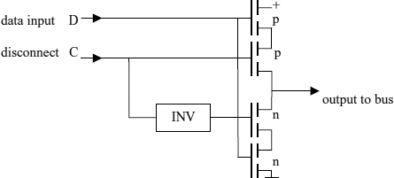
Figure 2.14 Tri-state output circuit
A simplified version of the tri-state output circuit connected to a bus line is the ‘open-drain’ output that results from replacing the p-channel transistors driving the output to the H level by a single pull-up resistor for the bus line. Several open-drain outputs may be connected to the same bus line. Several outputs may be on and drive the bus to the L level simultaneously. The level on the bus is the result of an AND applied to the individual outputs as in Figure 2.14 within a gate. The AND performed by wiring to a common pull-up resistor is called the ‘wired AND’. An open drain output can be simulated by a tri-state output buffer that uses the same input for data and to disconnect.
The CMOS building blocks explained so far are reactive in the sense of shown in section 1.4.3 After the processing time they keep their output if the inputs do not change. Complex circuits composed from the basic CMOS gates are also reactive. They are usually applied so that their input remains unchanged within the processing time, i.e. without attempting to exploit their throughput that may be higher. Circuits suitable for raising the throughput via pipelining must be given a layered structure (see Figure 1.12) by adding buffers if necessary. Then they also have the advantage that they do not go through multiple intermediate output changes (hazards) that otherwise can arise from operands to a gate having different delays w.r.t. the input.
2.1.2 Registers and Synchronization Signals
Besides the computational elements which can now be constructed from the CMOS gates according to appropriate algorithms (further discussed in Chapter 4), storage elements (registers) have been identified in section 1.4 as an essential prerequisite to building efficient digital systems using pipelining and serial processing.
A simple circuit to store a result value for a few ms from a starting event is the tri-state output (Figure 2.14) or the output of a transmission gate driving a load capacitance (attached gate inputs). Once the output is switched to the high-impedance state, the load capacitor keeps its voltage due to the high impedance of the gate inputs and the output transistors in their ‘off’ state. Due to small residual currents, the output voltage slowly changes and needs to be refreshed by driving the output again at a minimum rate of a few 100 Hz if a longer storage time is required. This kind of storage element is called ‘dynamic’. If the inverter inside the tri-state output circuit can be shared between several storage elements (e.g., in a pipeline), only two transistors are required for this function.

Figure 2.15 Pipelining with tri-state buffers or pass gates used as dynamic D latches

Figure 2.16 Dynamic master-slave D flip-flop
Figure 2.15 shows how a pipeline can be set up using dynamic storage and a periodic clock as in Figure 1.16. The required tri-state outputs can be incorporated into the compute circuits or realized as separate circuits (called dynamic ‘D latches’). The input to the compute circuits is stable during the ‘off’ phase of the clock signal when the transmission gates are high-impedance. In the ‘on’ phase they change, and the compute circuit must not follow these changes before the next ‘off’ time but output the result of the previous input just before the next ‘off’ time at the latest (the clock period must be larger than the processing time). This would hold if the compute circuit has a layered structure operated in a non-pipelined fashion.
If the output follows the input changes too fast, one can resort to using two non-overlapping clocks, one to change the input and one to sample the output. Then the input data are still unchanged when the output gets stored. The output latch is the input latch of the next stage of the pipeline. A simple scheme is to connect two complementary clocks to every second set of output latches which, however, implies that the input ‘on’ phase cannot be used for processing (the dotted clock in Figure 2.15 is the complementary one).
Alternatively, the input to the next pipeline stage can be stored in a second storage element during the time the output of the previous one changes, which is the master–slave storage element shown in Figure 2.16 that provides input and output events at the L-to-H clock edges only as discussed in Section 1.4.3. The clock signal for the second (slave) storage element is the inverse of the first and generated by the inverter needed for the first. While the first (master) storage element can be a transmission gate or the tri-state function within the data source, the second cannot be realized as a transmission gate as this would discharge the storage capacitor but needs an additional inverter or buffer stage (see Figure 2.14). Then a total of 8 transistors are needed to provide the (inverting) register function. From the inverter the dynamic D flip-flop also has a non-zero propagation delay or processing time from the data input immediately before the L-to-H clock edge to the data appearing at the output.
With the master-slave elements the input data are stable during the full clock period and the compute circuit can use all of the period for its processing except for the processing time of the flip-flop without special requirements on its structure. If the circuit in the pipeline is a single gate, the flip-flop delay would still inhibit its efficient usage as in the case of the two-phase sampling scheme.

Figure 2.17 Pipeline stage using dynamic logic
The tricky variant shown in Figure 2.17 (called ‘dynamic logic’) implements a single gate plus D flip-flop pipeline stage with just 5 transistors for the flip-flop function and further reduces the hardware complexity of the gate by eliminating the pull-up network. When the clock is L, the inner capacitor is charged high but the output capacitor holds its previous value. In the H phase the data input to the gates of the switch network must be stable to discharge the inner capacitor again to L if the network conducts, and the output capacitor is set to the resulting value. The processing by the gate and the loading of the output occur during the H phase of the clock, while the n-channel switch network is idle during the L phase. The next stage of the pipeline can use an inverted clock to continue to operate during the L phase when stable data are output. Alternatively, the next stage can use the same clock but a complementary structure using a p-channel network. The simplest case for the n- or p-channel network is a single transistor. Then the stage can be used to add delay elements into a complex circuit (called shimming delays) to give it a layered structure to enable pipelining.
One can hardly do better with such little hardware. If the n-channel network were to be operated at the double rate, the input would have to change very fast. The idle phase is actually used to let the inputs transition (charge the input capacitance to the new value). Dynamic logic is sometimes used in conjunction with static CMOS circuits to realize complex functions with a lower transistor count.
Static storage elements that hold their output without having to refresh it are realized by CMOS circuits using feedback and require some more effort. Boolean algorithms correspond to feed forward networks of gates that do not contain cycles (feedback of an output). If feedback is used for the CMOS inverter by wiring its output to the input, it cannot output an H or L level as none of them is a solution to the equation
![]()
In this case the output goes between the L and H levels and the inverter input (and output) is forced to the steep region of the VG − VD characteristic (see Figure 2.5) where it behaves like an analogue amplifier. For the non-inverting driver built from two inverters put in series, the feedback equation
![]()
has the two solutions L and H. The circuit composed of two CMOS inverters remains infinitely in each of these output states as the flipping to the other state would require energy to charge the output capacitance until it leaves the initial interval, overcoming the discharge current of the active output transistor that does not switch off before the double inverter delay. This 4-transistor feedback circuit is thus a storage element keeping its output value through time. If the energy is applied by briefly connecting a low impedance source to one of the outputs (e.g., from a tri-state output), the feedback circuit can be set into any desired state that remains stored afterwards. Actually, the needed amount of energy can be made very small by applying the feedback from the second inverter through a high resistor or equivalently by using transistors with a high on resistance for it (Figure 2.18) which is sufficient to keep the input capacitance to the first inverter continuously charged to H or L (there is no resistive load otherwise). An immediate application is to keep the last value driven onto a bus line to avoid the line being slowly discharged to levels outside L and H where gates inputting from the bus might start to draw current (see Figure 2.5).

Figure 2.18 Simple static storage element
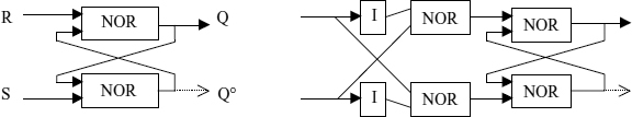
Figure 2.19 The RS flip-flop (NOR version) and the MRS gate
The combination of Figures 2.14 and 2.18 (the dynamic D latch and the bus keeper circuit) is the so-called D latch (usually, an inverter is added at the output). To set the output value Q from the first inverter in Figure 2.18 to the value presented at the data input D, one needs to apply the L level to the disconnect input C for a short time. Thereafter Q does not change. During the time when the disconnect input is L, the D latch is ‘transparent’. The data input value is propagated to the output and the output follows all changes at the input. This may be tolerable if the input data do not change during this time which may be kept very short and may even be required in some applications.
There are many other ways to implement storage elements with feedback circuits. The feedback circuit in Figure 2.19 built from 2 NOR gates (8 transistors) allows the setting of the output to H or L by applying H to the S or R input. It is called the RS flip-flop. It performs its output changes in response to the L-to-H transitions on R or S. A similar behavior results if NAND gates are used instead of the NOT gates (L and H become interchanged). A similar circuit having three stable output states and three inputs to set it into each of these can be built by cross-connecting three 3-input NOR gates instead of the two 2-input gates.
An RS flip-flop can be set and reset by separate signals but requires them not to become active simultaneously. A similar function often used to generate handshaking signals is the so-called Muller C gate with one input inverted (called MRS below) which differs from the RS flip-flop by also allowing the H-H input and not changing the output in that case. It can be derived from the RS flip-flop by using two extra NOR gates and two inverters to suppress the H-H input combination.
The register storing input data at the positive edges of a control signal (see Figure 1.15) without any assumptions about their frequency, and holding the output data for an unlimited time, can be derived from the static D latch. To pass and hold the input data present at the positive clock edge but not change the output before is done by cascading two D latches into the master–slave D flip-flop and using a complementary clock for the second as already shown in Figure 2.16 for the dynamic circuit. While the first stage opens to let the input data pass, the second stage still holds the previous output. At the positive edge the first stage keeps its output which is passed by the second. The inverted clock signal is already generated in the first D latch. Thus 18 transistors do the job, or 14 if pass gates are used instead of the tri-state circuits.
The (static) D flip-flop is the standard circuit implementing the sampling of digital signals at discrete times (the clock events). Banks of D flip-flops are offered as integrated components to sample and store several signals in parallel, also in combination with tri-state outputs. The timing of a static D flip-flop is similar to that of the dynamic flip-flop, i.e. a small processing time is required to pass the input data to the output after the clock edge. For commercial components the timing is referenced to the positive clock edge (for which a maximum rise time is specified) so that input data must be stable in between the set-up time before the edge and the hold time after the edge. The new output appears after a propagation delay from the clock edge.
Apart from these basic storage circuits feedback is not used within Boolean circuits. Feedback is, however, possible and actually resolved into operations performed at subsequent time steps if a register is within the feedback path (Figure 2.20). If the consecutive clock edges are indexed, xi is the input to the Boolean circuit from the register output between the edges i, i + 1, and ei is the remaining input during this time the output f(xi, ei) of the Boolean circuit to the register input is not constrained to equal xi but will be the register output after the next clock edge only, i.e.:
Circuits of this kind (also called automata) have many applications and will be further discussed in Chapter 5. If e.g. the xi are number codes and xi+1 = xi + 1, then the register outputs consecutive numbers (functions as a clock edge counter). The simplest special case are single bit numbers stored in a single D flip-flop and using an inverter to generate xi+1 = xi + 1 = (xi)° (Figure 2.21). After every L-to-H clock edge the output transitions from H to L or from L to H and toggles at half the clock frequency.

Figure 2.20 Feedback via a register

Figure 2.21 Single bit counter

Figure 2.22 Shift register

Figure 2.23 D flip-flop clocked at both edges
Another example of an automaton of this kind is the n-bit shift register built from n D flip-flops put in series (Figure 2.22). At the clock edge the data values move forward by one position so that if ei is the input to the first flip-flop after the ith edge, the n-tuple output by the shift register is (ei − 1,ei − 2,…,ei − n+1). The shift register is a versatile storage structure for multiple, subsequent input values that does not need extra circuits to direct the input data to different flip-flops or to select from their outputs. If the shift register is clocked continuously, it can be built using dynamic D flip-flops of 8 transistors each (6 if dynamic logic is employed).
If instead of just the L-to-H transitions of a ‘unipolar’ clock, both transitions are used, then the clock signal does not need not return to L before the next event, and this ‘bipolar’ clock can run at a lower frequency. Also, two sequences of events signaled by the bipolar clock sources c, c′ can be merged by forming the combined bipolar clock XOR(c, c′) (nearly simultaneous transitions would then be suppressed, however). An L-to-H only unipolar clock signal is converted into an equivalent bipolar one using both transitions with the 1-bit counter (Figure 2.21), and conversely by forming the XOR of the bipolar clock and a delayed version of it. A general method for building circuits that respond to the L-to-H edges of several unipolar clock signals is to first transform the clocks into bipolar ones signaling at both transitions and then merging them into a single bipolar clock.
Figure 2.23 shows a variant of the D flip-flop that samples the input data on both clock edges. The D latches are not put in series as in the master–slave configuration, but in parallel to receive the same input. The inverter is shared by the latches and the select gate.
The auxiliary circuits needed to provide handshaking signals (see Figure 1.18) to a compute building block can be synthesized in various ways from the components discussed so far [7, 39]. In order not to delay the input handshake until the output is no longer needed, and to implement pipelining or the ability to use the circuit several times during an algorithm, a register also taking part in the handshaking is common for the input or output. If a certain minimum rate can be guaranteed for the application of the building block, dynamic storage can be used. A building block that can be used at arbitrary rates requires static storage elements. The handshaking signals can be generated by a circuit that runs through their protocol in several sequential steps synchronized to some clock, but at the level of hardware building blocks simpler solutions exist. Due to the effort needed to generate the handshake signals, handshaking is not applied to individual gates but to more complex functions.

Figure 2.24 Handshake generation
Handshaking begins with the event of new input data that is signaled by letting IR perform its L-to-H transition. After this event the IR signal remains active using some storage element to keep its value. It is reset to the inactive state in response to another event, namely the IA signal transition, and hence requires a storage circuit that responds to two clock inputs. If IR and IA were defined to signal new data by switching to the opposite level (i.e., using both transitions), they would not have to be reset at all and could be generated by separately clocked flip-flops. This definition of the handshaking signals is suitable for pipelining but causes difficulties when handshaking signals need to be combined or selected from different sources.
The generic circuit in Figure 2.24 uses two MRS flip-flops to generate IA and OR. It is combined with an arbitrary compute function and a storage element for its data output (a latch freezing the output data as long as OR is H, maybe just by tri-stating the output of the compute circuit). The OR signal also indicates valid data being stored in the data register. The rising edge of the IR signal is delayed corresponding to its worst case processing delay of the compute circuit by a delay generator circuit while the falling edge is supposed to be passed immediately. A handshaking cycle begins with IA and IR being L. IR goes H, and valid data are presented at the input at the same time. After the processing delay the rising edge of IR is passed to the input of the upper MRS gate. It responds by setting IA to the H level as soon as the OR signal output by the lower MRS gate has been reset by an OA pulse. The setting of IA causes OR to be set again once OA is L, and thereby latches the output data of the compute that have become valid at that time. IA is reset to L when the falling edge of IR is passed to the upper MRS gate. Alternatively, the compute and delay circuits may be placed to the right of the MRS gates and the data register which then becomes an input register.
To generate the delay for a compute circuit that is a network of elementary gates, one can employ a chain of inverters or AND gates (then the delay will automatically adjust to changes of the temperature or the supply voltage). If the circuit is realized by means of dynamic logic or otherwise synchronized to a periodic clock signal, the delay can be generated by a shift register or by counting up to the number of clock cycles needed to perform the computation (an unrelated fast clock could also serve as a time base). Some algorithms may allow the delayed request to be derived from signals within the circuit.
2.1.3 Power Consumption and Related Design Rules
A CMOS circuit does not consume power once the output capacitance has been loaded and all digital signals have attained a steady state close to the ground level or the power supply level and transistor switches in the ‘open’ state really do not conduct. Actually a small quiescent current remains, but less than 1% of the power consumption of a system based on CMOS technology is due to it typically at the current supply voltage levels.
Another part of the total power consumption, typically about 10%, is due to the fact that for gate inputs in the intermediate region between L and H both the n-channel and p-channel transistors conduct to some degree (Figure 2.5). Inputs from a high impedance source (e.g., a bus line) may be kept from discharging into the intermediate region by using hold circuits (Figure 2.18) but every transition from L to H or vice versa needs to pass this intermediate region. The transition times of the digital signals determine how fast this intermediate region is passed and how much power is dissipated during the transitions. Using equation (4) in section 2.1.1, they are proportional to the capacitance driven by the signal source. If f are the frequency of L-H transitions at the inverter input, t the time to pass between L to H and j the mean ‘cross-current’ in that region, then the mean current drawn from the supply is:
To keep this current low, load capacitances must be kept low, and high fan-outs must be avoided. If N inverter inputs need to be driven by a signal, the load capacitance is proportional to N and the cross-current through the N inverters becomes proportional to N2. If a driver tree is implemented (Figure 2.9), about 2N inverter inputs need to be driven, but the rise time is constant and the cross-current is just proportional to N.
The major part of the power consumption is dissipated during the changes of the signals between the logic levels to charge or discharge the input and output capacitances of the gates. To charge a capacitor with the capacitance C from zero to the supply voltage U, the applied charge and energy are:
Half of this energy remains stored in the capacitor while the other half is dissipated as heat when the capacitor is charged via a transistor (or a resistor) from the supply voltage U. If the capacitor is charged and discharged with a mean frequency f, the resulting current and power dissipation are:
This power dissipation may set a limit to the operating frequency of an integrated circuit; if all gates were used at the highest possible frequency, the chip might be heated up too much even if extensive cooling is applied. Semiconductor junctions must stay below 150°C. The junction temperature is warmer than the surface of the chip package by the dissipated power times the thermal resistance of the package.
Equations (7) and (8) also apply if the capacitor is not discharged or charged to the supply voltage but charged by an amount U w.r.t. to an arbitrary initial voltage and then discharged again to this initial voltage through resistors or transistors connected to the final voltage levels to supply the charge or discharge currents. U cannot be reduced arbitrarily for the sake of a reduced power consumption as some noise margin is needed between the H and L levels. The voltage swing can be lowered to levels to a few 100 mV if two-line differential encoding is used for the bits (i.e. a pair of signals driven to complementary levels) by exploiting the common mode noise immunity of a differential signal. If the inputs to a Boolean circuit implementing an algorithm for some function on the basis of gate operations are changed to a new bit pattern, after the processing time of the circuit, all gate outputs will have attained steady values. If k gate inputs and outputs have changed from L to H, the energy for the computation of the new output is at least
if the capacitances at all gate inputs and outputs are assumed to be equal to C and the actual values within the L and H intervals are zero and U. It becomes higher if there occur intermediate changes to invalid levels due to gate delays. These may be determined through an analysis or a simulation of the circuit and are only avoided in a layered circuit design with identical, data-independent gate delays. If the computation is repeated with a frequency f, and k is the mean number of bit changes for the applied input data, then the power dissipation is P = E*f. The power dissipation depends both on the choice of the algorithm and the applied data. Different algorithms for the same function may require different amounts of energy. The number k of level changes does not depend on whether the computation is performed by a parallel circuit or serially. As a partially serial computation needs auxiliary control and storage circuits, it will consume more energy than a parallel one.
Equation (8) depends on the fact that during the charging of the capacitor a large voltage (up to U) develops across the resistor. If during the loading process the voltage across the resistor is limited to a small value by loading from a ramp or sine waveform instead of the fixed level U, the energy dissipated in the resistor of transistor can be arbitrarily low. The capacitor can be charged by the constant current I to the level of U in a time of T = UC/I. During this time the power dissipated by the resistor is N = RI2 and the energy dissipated during T becomes:
If before and after a computation the same number of signal nodes with capacitances C w. r. t. to the ground level are at the H level, then theoretically the new state could be reached without extra energy as the charges in the capacitors are just redistributed at the same level of potential energy. This would always be the case if input and output codes are extended by their complements and the Boolean circuit is duplicated in negative logic or implemented from building blocks as shown in Figure 2.12 (then NOT operations can be eliminated, too, that otherwise introduce data-dependent processing delays). ‘Adiabatic’ computation through state changes at a constant energy level also plays a role in the recent development of quantum computing [8].
Figure 2.25 shows a hypothetical ‘machine’ exchanging the charges of two capacitors (hence performing the NOT function if one holds the bit and the other its complement) without consuming energy. Both capacitors are assumed to have the capacitance C, the capacitors and the inductance are ideal, and the switch is ideal and can be operated without consuming energy. At the start of the operation C1 is supposed to be charged to the voltage U while C2 is discharged. To perform the computation, the switch is closed exactly for the time of T = 2−1/2π(LC)1/2. At the end C2 is charged to U and C1 is discharged. After another time of T the NOT computation would be undone. In practical CMOS circuits, the energy stored in the individual load capacitors cannot be recovered this way (unless a big bus capacitance were to be driven), but a slightly different approach can be taken to significantly reduce the power consumption.
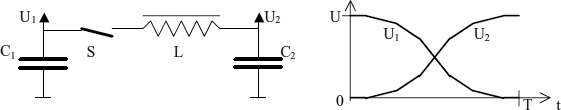
Figure 2.25 Zero-energy reversible NOT operation
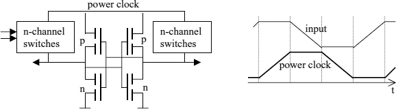
Figure 2.26 Adiabatic CMOS gate
The option to move charges between large capacitors, without a loss of energy, can be exploited by using the sine waveform developing during the charge transfer to smoothly load and discharge sets of input and output capacitors with a small voltage drop across the charging resistors or transistors, as explained above. Thus, the DC power supply is substituted by a signal varying between zero and a maximum value U (a ‘power clock’). Circuits relying on smoothly charging or discharging from or to a power clock are called adiabatic. Various adiabatic circuit schemes have been implemented [37, 38]. A simplified, possible structure of an adiabatic CMOS gate with two complementary n-channel switch networks and complementary outputs is shown in Figure 2.26. During the charging of the output capacitors the logic levels at the transistor gates are assumed to be constant. This can be achieved in a pipelined arrangement where one stage outputs constant output data using a constant supply voltage while the next one gets charged by smoothly driving up its supply. Once charged, the gate keeps its state even while its input gets discharged due to the feedback within the gate circuit. Using equation 10, the energy dissipated by an adiabatic computation can be expected to be inversely proportional to the execution time T (~ I−1), and the current consumption to decrease such as T−2 instead of just T−1 as for standard CMOS circuits clocked at a reduced rate. Practically, only a fraction of these savings can be realized, but enough to make it an interesting design option. The charge trapped in the intermediate nodes of the switch networks cannot be recycled unless all inputs are maintained during the discharging, and the discharging through the p-channel transistors only works until the threshold voltage is reached. Low capacitance registers can be added at the outputs as in Figure 1.16 to avoid the extensive input hold times.

Figure 2.27 Ripple-carry counter
Storage elements are built from CMOS gates and also dissipate power for the output transitions of each of them. A latch uses a smaller number of gates and hence consumes less power than a flip-flop. In a master-slave flip-flop the clock is inverted so that every clock edge leads to charging some internal capacitance C′ even if the data input and output do not change. Thus just the clocking of an n-bit data register at a frequency f continuously dissipates the power of
Registered circuits implemented with dynamic logic (see Figure 2.17) consume less power than conventional CMOS gates combined with latches or master–slave registers. If the clock is held at the L level, then there are no cross-currents even if the inputs discharge to intermediate levels.
In order to estimate the continuous power consumption of a subsystem operating in a repetitive fashion one needs to take into account that the transition frequencies at the different gate inputs and outputs are not the same. The circuit shown in Figure 2.27 is a cascade of single bit counters as shown in Figure 2.21 obtained by using the output of every stage as the clock input of the next. This is called the ripple counter and serves to derive a clock signal with the frequency f/2n from the input clock with the frequency f. Each stage divides the frequency by 2. If I0 is the current consumed by the first stage clocked with f, then the second stage runs at half this frequency and hence consumes I0/2, the third I0/4 etc. The total current consumption of the n-stage counter becomes:
![]()
The technique of using a reactive Boolean circuit with input and output registers clocked at a rate higher than the processing time of the circuit (see section 1.4.3) in order to arrive at a well-defined timing behavior thus leads to continuous power consumption proportional to the clock rate. Some techniques can be used to reduce this power consumption:
- Avoid early, invalid signal transitions and the secondary transitions that may result from them by using layered circuits.
- Use data latches instead of master–slave registers, maybe using an asymmetric clock with a short low time.
- Suppress the clock by means of a gate if a register is not to change, e.g. for extended storage or if the input is known to be unchanged.
- Use low level differential signals for data transfers suffering from capacitive loads.
The gating of a clock is achieved by passing it through an OR (or an AND) gate. If the second input is H (L for the AND gate), H (L) is selected for the gate output. The control signal applied to the second input must not change when the clock signal is L (H).
If the power consumption is to be reduced, the frequency of applying the components (the clock frequency for the registers) must be reduced and thereby the processing speed, the throughput and the efficiency (the fraction of time in which the compute circuits are actually active). The energy needed for an individual computation does not change and is proportional to the supply voltage U. The energy can only be reduced and the efficiency can be maintained by also lowering U. Then the transistor switches get a higher ‘on’ resistance and the processing time of the gate components increases. The ‘on’ resistance is, in fact, inversely proportional to U−UT where U denotes the supply voltage and UT is the threshold voltage (see section 2.1.1). Then the power consumption for a repeated computation becomes roughly proportional to the square of the clock frequency. If the required rate of operations of a subsystem significantly varies with time, this can be used to dynamically adjust its clock rate and the supply voltage so that its efficiency is maintained. The signals at the interface of the subsystem would still use some standard voltage levels. This technique is common for battery-powered computers, but can be systematically used whenever a part of a system cannot be used efficiently otherwise. A special case is the powering down of subsystems that are not used at all for some time.
The use of handshaking between the building blocks of a system can also serve to reduce the power consumption. Instead of a global clock, individual clocks are used (the handshake signals) that are only activated at the data rate really used for them. A handshaking building block may use a local clock but can gate it off as long as there are no valid data. This is similar to automatically reducing the power consumption of unused parts of the system (not trying to using them efficiently). If the processing delay for a building block is generated by a chain of inverters, the estimating delay adapts to voltage and temperature in the same way as the actual processing time. It then suffices to vary the voltage to adjust the power dissipation, and the handshake signals (the individual clocks) adjust automatically. A control flow is easily exploited by suppressing input handshake to unused sub-circuits. Similar power-saving effects (without the automatic generation and adjustment of delays) can, however, also be obtained with clocked logic by using clock gating.
2.1.4 Pulse Generation and Interfacing
Besides the computational building blocks and their control, a digital system needs some auxiliary signals like a power-on reset signal and a clock source that must be generated by appropriate circuits, and needs to be interfaced to the outside world, reading switches and driving loads. In this section, some basic circuits are presented that provide these functions. Interfaces to input and output analogue signals will follow in Chapter 8. For more details on circuit design we refer to [19].
The most basic signal needed to run a digital system (and most other electronic circuits) is a stable DC power supply delivering the required current, typical supply voltages being 5.0V, 3.3V for the gates driving the signals external to the chips and additionally lower voltages like 2.5V, 1.8 V, 1.5V, and 1.2V for memory interfaces and circuits within the more recent chips. In many applications, several of these voltages need to be supplied for the different functions. To achieve a low impedance at high frequencies the power supply signals need to be connected to grounded capacitors close to the load sites all over the system.
A typical power supply design is to first provide an unregulated DC voltage from a battery or one derived from an AC outlet and pass it through a linear or a switching regulator circuit. Regulators outputting e.g. a smooth and precise 5V DC from an input ranging between 7-20V with an overlaid AC ripple are available as standard integrated 3-terminal circuits. The current supplied at the output is passed to it from the input through a power transistor within the regulator. For an input voltage above 10V, more power is dissipated by this transistor than by the digital circuits fed by it. A switching regulator uses an inductance that is switched at a high frequency (ranging from 100 kHz to several MHz) to first store energy from the input and then to deliver it at the desired voltage level to the output. It achieves a higher efficiency (about 90%, i.e. consumes only a small fraction of the total power by itself) and a large input range. Switching regulators can also be used to convert from a low battery voltage to a higher one (Figure 2.28). The switches are implemented with n-channel and p-channel power MOS transistors having very low resistances (some 0.1Ω). The transistor switches are controlled by digital signals. Single and multiple regulators are available as integrated circuits including the power transistors.

Figure 2.28 Switching down and up regulator configurations
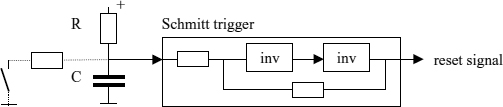
Figure 2.29 Reset signal generation using a Schmitt trigger circuit
A high efficiency voltage converter deriving the voltage Θ/2 from a supply voltage Θ can be built by using a switched capacitor only that is connected between the input and the output terminals to get charged by the output current, or alternatively between the ground reference and the output terminal to get discharged by the load current. The two connections are made by low resistance transistor switches and alternate at a high frequency so that a small voltage change U develops and the power dissipation is low due to equations (7) and (8) in the previous section. The input delivers the load current only at half time.
After power-up, some of the storage elements in a digital system must usually be set to specific initial values which is performed in response to a specific input signal called a reset signal. It is defined to stay at a specific level, say L, for a few ms after applying the power and then changes to H. An easy way to generate a signal of this kind is by means of a capacitor that is slowly charged to H via a resistor. In order to derive from a digital signal that makes a fast transition from L to H, the voltage across the capacitor can be passed through a CMOS inverter that is used here as a high gain amplifier. If feedback is implemented as in Figure 2.29 a single transition results even if the input signal or the power supply is overlaid with some electrical noise. The reset circuit outputs the L level after power-up that holds for some time after the power has reached its full level depending on the values for C and the resistors (usually its duration does not need be precise). The switch shown as an option permits a manual reset by discharging the capacitor.

Figure 2.30 Crystal oscillator circuit
The buffer circuit with a little amount of feedback to the input is a standard circuit known as the Schmitt trigger that is used to transform a slow, monotonic waveform into a digital signal. Its Vin − Vout characteristic displays a hysteresis. The L-H transition occurs at a higher input level than the H-L transition. The actual implementation would realize the feedback resistor from the output by simply using transistors with a high on resistance. The other one can be substituted by a two transistor non-inverting input stage (similar to Figure 2.5 but with the n- and p-channel transistors interchanged).
A periodic clock signal as needed for clocking the registers and as the timing reference within a digital system is easily generated using the CMOS inverter circuit as a high gain amplifier again and using a resonator for a selective feedback at the desired frequency. The circuit in Figure 2.30. uses a piezoelectric crystal for this purpose and generates a full swing periodic signal at its mechanical resonance frequency which is very stable (exhibits relative frequency deviations of less than 10−7 only) and may be selected in the rage of 30 kHz…60 MHz through the mechanical parameters of the crystal. The resistor serves to let the amplifier operate at the midpoint of its characteristic (Figure 2.5), and the capacitors serve as a voltage divider to provide the phase shift needed for feedback. The second inverter simply amplifies the oscillator output to a square waveform with fast transitions between L and H. Crystals are offered commercially at any required frequencies, and complete clock generator circuits including the inverters are offered as integrated components as well.
The frequency of a crystal oscillator cannot be changed but other clock signals can be derived from it by means of frequency divider circuits. A frequency divider by two is provided by the circuit shown in Figure 2.21 using a D flip-flop and feeding back its inverted output to its data input. Then the output becomes inverted after every clock edge (plus the processing delay of the flip-flop), and the resulting signal is a square wave of half the clock frequency h and a 50% duty cycle, i.e. the property that the L and H times are identical (this is not guaranteed for the crystal oscillator output). If several frequency dividers of this kind are cascaded so that the output of a divider becomes the clock input for the next stage, one obtains a frequency divider by 2n, the ripple-carry counter already shown in Figure 2.27. As each of the flip-flops has its own clock their clock edges do not occur simultaneously.
To divide the input frequency h by some integer k in the range 2n−1 < k ≤ 2n, a modified edge counter circuit can be used, i.e. an n-bit register with a feedback function f that performs the n-bit binary increment operation f(x) = x + 1 as proposed in section 2.1.2 (also called a synchronous counter as all flip-flops of the register here use the same clock signal), but only for x < k − 1, whereas f(k − 1) = 0. Then the register cycles through the sequence of binary codes of 0,1,2,…,k-1 and the highest code bit is a periodic signal with the frequency h/k.

Figure 2.31 Fractional frequency divider

Figure 2.32 PLL clock generator
Another variant is the fractional counter that generates the multiple h*k/2n for a non-negative integer k < 2n−1 (Figure 2.31). This time the feedback function is f(x) = x + k (algorithms for the binary add operation follow in section 4.2). The output from the highest code bit is not strictly periodic at the prescribed frequency (for odd k, the true repetition rate is h/2n). The transitions between L and H remain synchronized with the input clock and occur with a delay of at most one input period.
The frequency dividers discussed so far generate frequencies below ½h only. It is also useful to be able to generate a periodic clock at a precise integer multiple k of the given reference h. The crystal oscillators do not cover clock frequencies of the several 100 MHz needed for high speed processors but their frequencies might be multiplied to the desired range. It is quite easy to build high frequency voltage-controlled oscillators (VCO), the frequencies of which can be varied over some range by means of control voltages moving continuously over a corresponding range. The idea is to control the frequency q of a VCO so that q / k = h (a signal with the frequency q/k is obtained from a frequency divider). The deviation is detected by a so-called phase comparator circuit and used to generate the control voltage, setting up a phase-locked loop (PLL, Figure 2.32). If the VCO output is divided by m, then the resulting output frequency becomes k/m* h.
The phase comparator (PC in Figure 2.32) can be implemented as a digital circuit that stores two bits encoding the numbers 0, 1, 2, 3 and responds to the L-to-H transitions at two separate clock inputs. The one denoted ‘+’ counts up to 3, and the one denoted ‘−’ counts down to 0. The phase comparator outputs the upper code bit, i.e. zero for 0, 1 and the supply voltage for 2, 3. If the frequency of the VCO is higher than k*h, there are more edges counting down and PC is in one of the states 0, 1 and outputs the zero level which drives the VCO frequency down. If the reference clock is higher, it is driven up. If both frequencies have become equal, the state alternates between 1, 2 and the mean value of the output voltage depends on their relative phase which becomes locked at some specific value. The R-R′-C integrator circuit needs to be carefully designed in order to achieve a fast and stable control loop [40]. The VCO output can then be passed through a divide by m counter to obtain the rational multiple of the reference clock frequency by k/m.
Input data to a digital system must be converted to the H and L levels required by the CMOS circuits. The easiest way to input a bit is by means of a mechanical switch shorting a H level generated via a resistor to ground. Mechanical make switches generate unwanted pulses before closing due to the jumping of the contact, which are recognized as separate edges if the input is used as a clock. Then some pre-processing is necessary to ‘debounce’ the input. The circuit in Figure 2.29 can be used, or a feedback circuit like the RS flip-flop or the hold circuit in Figure 2.18 that keeps the changed input value from the first pulse (but needs a separate switch or a select switch to be reset).
Data input from other machines is usually by means of electrical signals. If long cabling distances are involved, the L and H levels used within the digital circuits do not provide enough noise margin and are converted to higher voltage levels (e.g. [3, 12]V to represent 0 and [−12, −3]V to represent 1) or to differential signals by means of input and output amplifiers that are available as integrated standard components. For differential signals the H and L levels can be reduced to a few 100 mV. At the same time the bit rates can be raised. The LVDS signaling standard (‘low voltage differential signaling’) e.g. achieves bit rates of 655 M bit/s and, due to its low differential voltages of ±350 mV, operates from low power supply voltages [21]. LVDS uses current drivers to develop these voltages levels across 100Ω termination resistors. Variants of LVDS support buses and achieve bit rates beyond 1 Gbit/s. An LVDS bus line is terminated at both ends and therefore needs twice the drive current.
If systems operating at different ground levels need to be interfaced, the signals are transferred optically by converting a source signal by means of a light emitting diode that is mounted close to a photo transistor converting back to an electrical signal. Such optoelectronic couplers are offered as integrated standard components as well (alternatively, the converters are linked by a glass fiber replacing the cable).
The switches, converters, cables, wires and even the input pins to the integrated circuits needed to enter data into a system are costly and consume space. The idea of reusing them in a time-serial fashion for several data transfers is applied in the same way as it was to the compute circuits. Again, this involves auxiliary circuits to select, distribute and store data. A common structure performing some of these auxiliary functions for the transfer of an n-bit code using a single-bit interface in n time steps is the shift register (Figure 2.22). After n time steps the code stands in the flip-flops of the register and can be applied in parallel as an input to the compute circuits. Figure 2.33 shows the resulting interface structure. The clock signal defines the input events for the individual bits and must be input along with the data (or generated from the transitions of the data input). If both clock edges are used, the interface is said to be a double data rate interface (DDR). No further handshaking is needed for the individual bits, but it is needed to define the start positions of multi-bit code words and must be input or be generated as well (at least, the clock edges must be counted to determine when the receiving shift register has been filled with new bits). The serial interface is reused as a whole to transfer multiple code words in sequence. The register, the generation of the clock and the handshake signals add up to a complex digital circuit that does not directly contribute to the data processing but can be much cheaper than the interface hardware needed for the parallel code transfer.

Figure 2.33 Serial interface structure (G: bit and word clock generator, C: signal converter)
The output from a digital system (or subsystem) to another one is by means of electrical signals converted to appropriate levels, as explained before. A serial output interface requires a slightly more complex register including input selectors to its flip-flops so that it can also be loaded in parallel in response to a word clock (Figure 2.33). If the data rate achieved with the bit-serial transfer is not high enough, two or four data lines and shift registers can be operated in parallel. Another option is to convert the interface signals into differential ones using LVDS buffers. Then much higher data rates can be achieved that compensate for the serialization of the transfer.
To further reduce the cables and wires the same can be used to transfer data words in both directions between the systems (yet at different times using some extra control). Finally, the clock lines can be eliminated. For an asynchronous serial interface each word transmission starts by a specific signal transition (e.g. L -> H) and the data bits follow this event with a prescribed timing that must be applied by the receiver to sample the data line. Another common method is to share a single line operating at the double bit rate for both the clock and the data by transmitting every ‘0’ bit as a 0-1 code and every ‘1’ as a 1-0 code (Manchester encoding), starting each transmission by an appropriate synchronization sequence. Then for every bit pattern the transmitted sequence makes many 0-1 transitions which can be used to regenerate the clock using a PLL circuit at the receive site. The effort to do this is paid for by the simplified wiring.
The CMOS outputs can directly drive light emitting diodes (LED) through a resistor that give a visible output at as little as 2mA of current (Figure 2.34). To interface to the coil of an electromechanical switch or a motor one would use a power transistor to provide the required current and voltage levels. When the transistor switches off, the clamp diode limits the induced voltage to slightly above the coil power supply voltage and thereby protects the transistor from excessive voltages. The same circuit can be used to apply any voltage between the coil power supply and zero by applying a high frequency, periodic, pulse width modulated (PWM) digital input signal to the gate of the transistor. To output a bipolar signal, ‘H’ bridge arrangements of power transistors are used. Integrated LED arrays or power bridges to drive loads in both polarities are common output devices.

Figure 2.34 Interfacing to LED lamps and coils
2.2 CHIP TECHNOLOGY
Since the late 1960s, composite circuits with several interconnected transistors have been integrated onto a silicon ‘chip’ and been packed into appropriate carriers supplying leads to the inputs and outputs of the circuit (and to the power supply). Since then the transistor count per chip has raised almost exponentially. At the same time, the dimensions of the individual transistors were reduced by more than two orders of magnitude. For the gate lengths the values decreased from 10 μm in 1971 to 0.1 μm in 2001. The first families of bipolar and CMOS integrated logic functions used supply voltages of 5V and above. A 100 mm2 processor chip filled with a mix of random networks of gates and registers and some memory can hold up to 5*107 transistors in 0.1 μ CMOS technology. For dedicated memory chips the densities are much higher (see section 2.2.2).
The technology used for a chip and characterized by the above feature size parameter s determines the performance level of a chip to a high degree. If a single-chip digital system or a component such as a processor is reimplemented in a smaller feature size technology, it becomes cheaper, faster, consumes less power, and may outperform a more efficient design still manufactured using the previous technology. Roughly, the thickness of the gate insulators is proportional to s. The supply voltage and the logic levels need to be scaled proportional to s in order to maintain the same levels for the electrical fields. For a given chip area, the total capacitance is proportional to s−1, the power dissipation P = U2Cf (formula (8) in 2.1.3) for an operating frequency f hence proportional to s, and f can be raised proportional to s−1 for a fixed power level. At the same time, the gate density grows with s−2.
A problem encountered with highly integrated chips is the limitation of the number of i/o leads to a chip package. Whereas early small-scale integrated circuits had pin counts of 8–16, pin counts can now range up to about 1000, but at considerable costs for the packages and the circuit boards. For chips with up to 240 leads surface-mount quadratic flat packages (QFP) are common from which the leads extend from the borders with spacing as low as ½ mm. To reduce the package sizes and to also support higher i/o counts, ball grid array (BGA) packages have become common where the leads (tiny solder balls) are arranged in a quadratic grid at the bottom side of the package and thus can fill out the entire area of the package. While a 240 pin QFP has a size of 32 × 32 mm, a BGA package with the same lead count only requires about 16 × 16 mm. For the sake of reduced package and circuit board costs, chips with moderate pin counts are desirable. Chips are complex hardware modules within a digital system. Generally, the module interfaces within a system should be as simple as possible. The data codes exchanged between the chips may be much wider than the number of signal lines between them anyhow by using serial data transfers in multiple time steps.
For large chips, testing is an issue and must be supported by their logic design. Although the manufacturing techniques have improved, isolated faulty transistors or gates can render a chip unusable unless the logic design provides some capabilities to replace them by spare operational ones (this is common for chips which contain arrays of similar substructures). Otherwise the ‘yield’ for large chips becomes low and lets the cost of operational ones increase. Chips are produced side by side on large silicon wafers (with diameters of 20 cm and above) from which they are cut to be packaged individually. The level of integration has been raised further in special applications by connecting the operational chips on a wafer without cutting it (wafer-scale integration). The array of interconnected chips on a wafer must support the existence of faulty elements.
The achievable complexity of integrated circuits is high enough to allow a large range of applications to be implemented on single chip digital processors, at least in principle. The high design and manufacturing costs of large-scale integrated circuits, however, prohibit single chip ASIC implementations except for very high volume products. Otherwise the digital system would be built from several standard or application specific chip components mounted and connected on one or several circuit boards. The standard chips and ASIC devices are the building blocks for the board level design, and the implementation of multi-chip systems on circuit boards provides the scalability required to cover both high performance or low volume applications. Chips always have a fixed, invariable structure. They can, however, be designed to offer some configurability to support more than one application or some design optimizations without having to redesign the hardware (by implementing combined functions in the sense discussed in Section 1.3.3).
The component chips can only be cost effective if they are produced in large volumes themselves which is the case if their respective functions are required in several applications, or if they can be programmed or configured for different applications. At the board level, reusable ‘standard’ subsystems are attractive, too, and the cost for board level system integration must be considered to compare different design options. Chips to be used as components on circuit boards benefit from integrating as many functions as possible and from having a small number of easy-to-use interface signals with respect to their timing and handshaking. In general, the interfacing of chips on a board requires pin drivers for higher signal levels than those inside the chips involving extra delays and power consumption related to their higher capacitive loads. If there is a choice of using a chip integrating the functions of two other ones, it will provide more performance and lower power consumption yet less modularity for the board level design.
For the internal and external interfaces of digital systems small-to-medium-scale standard or application-specific integrated circuits are used to provide the generation of the required signal levels and to perform digital functions to accommodate them to the interfacing standards of the digital processor. It is e.g. common to realize driver functions that adapt the internal digital signals to the voltages and currents required at the external interfaces in separate integrated circuits, both because they are the most likely places where damage can occur to a digital system (then only the drivers need to be exchanged) and because they use transistors with different parameters which are not easily integrated with the processing gates. Generally it is hard to integrate circuit structures with different, special characteristics, e.g. special memory technologies, random gate networks and analogue interfaces. Otherwise highly integrated components are predominant, starting from configurable standard interface functions.
In the subsequent sections some common highly integrated building blocks of digital systems will be presented that are usually packaged as chips or constitute large modules within still larger chips. Fixed function small-scale and medium-scale integrated circuits have lost much of their former importance and are often replaced by configurable components but some still play a role. If a few gates are needed-one can choose from small and cheap packages like those containing six CMOS inverters or four 2-input gates, and for interfacing to buses there are banks of tri-state drivers with or without keeper circuits and multi-bit latches and registers.

Figure 2.35 16-bit SRAM and Flash memory interface signals
Figure 2.36 Read and write cycle timing
2.2.1 Memory Bus Interface
Among the most prominent components of digital systems are the various kinds of memory chips. They are fixed configuration building blocks used in large volume. Memory is used for storing intermediate results, for holding the input and output data of computations, and to provide random access to data that came in serially. The flip-flops and registers introduced in section 2.1.2 can be extended by select and decode circuits to implement storage for multiple data words that can be selected via address signals. In many applications the storage requirements are for quite large numbers of data bits. Integrated memory chips offer a large numbers of individual, highly optimized multi-bit storage cells and the selection circuits.
The static random access memory (SRAM) and the ‘flash’ erasable and programmable read only memory (EPROM) chips or modules explained in the next section have the generic interface shown in Figure 2.35. The n address inputs A0,…,An−1 are used to select from 2n storage locations (common values for these chips are n = 16, 18), the control signals /OE (output enable), /WE (write enable), /CE (chip enable) transfer read and write commands, and the k data lines D0,…,Dk−1 that transfer k-bit data words during read or write operations (k = 8, 16). 16-bit devices usually have extra control signals /BLE and /BHE to activate the lower and upper 8-bit half (‘byte’) of the data word separately. Read and write operations are performed sequentially. During a read operation the data lines of the memory device are outputs. Otherwise the outputs are tri-stated. During a write operation the data lines input the data to be stored.
Read and write operations can be controlled most simply with /CE and /WE alone if the other control signals are held at the L level. Figure 2.36 shows the timing of the read operation from an SRAM or an EPROM and the SRAM write operation. The address inputs and /WE are signaled valid by the falling edge of /CE and do not change during the time /CE is low. Alternatively, /WE or /OE are pulsed low for the write and read operations while /CE is low. In the read cycle, the output data become available before the rising edge of /CE (/OE in the other scheme), some time after applying the address needed for the selection of the data (their arrival after the invalid data XX is not indicated by an extra signal). This time is referenced to the falling edge of /CE and specified as the access time of the particular memory device. The data can be stored in a register clocked with /CE (/OE) but disappear from the bus a short ‘hold’ time after /CE (/OE) is high again. In the write cycle the write data must be applied no later than a specific set-up time before the rising edge of /CE (/WE). After the rising edge of /CE the address lines may change for the next memory cycle.
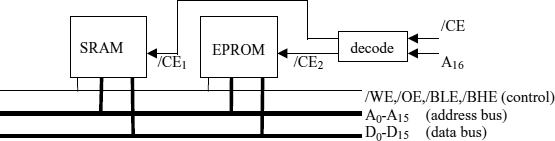
Figure 2.37 Multiple memory chips connected to a bus
Several memory chips of different kinds and sizes can be connected to the same sets of data and address lines (‘buses’) provided that their /CE signals do not become active and read operations are not carried out simultaneously on several devices (Figure 2.37). The data and address words are transferred to all memory chips using the same signal lines. The individual /CE signals are generated by means of a decoder circuit (a few CMOS gates) in response to additional address signals.
An important parameter of the memory interface is the number of data lines which determines how many bits can be transferred simultaneously (performance), and how many wires and signal drivers are needed (cost). A 16-bit code required as a parallel input to a circuit can be loaded from a memory via an 8-bit data bus but this takes two bus cycles and requires the first byte to be stored in a register until the second is ready, too (if there was just one data line, one would arrive at a bit-serial interface to the memory and have to use a shift register as in Figure 2.33). Thus transfer speed can be traded off for a simpler interface.
A 16-bit memory device can be connected to an 8-bit data bus, too. If /BLE and /BHE are never activated simultaneously, the lower and upper bytes can be tied together and connected to the data bus. Also, several memory modules with a small number of data lines can be connected in parallel to the same address and control signals but to different data bus lines to yield a wider memory structure. The bus with the multiple memory devices connected to it and the inputs to the address decoder behaves like a single memory device with the generic interface.
Another way to trade off performance against lower cost for the interfacing is to use the same signal lines to transfer the addresses and the data. Then an extra time step is needed for the address transfer, and the address must be latched for the subsequent read or write operation using an extra address latch enable control signal (ALE, Figure 2.38). A bus with common address and data lines is called a multiplexed bus. On it, every memory operation needs two transfers via the bus, and for the attached memory devices the address latches must be provided. If they are integrated into the memory chips, the pin count is reduced significantly.
There are many cases in which the addresses of subsequent memory accesses follow some standard pattern, e.g. obtained by performing a binary increment (add 1) operation. This can be exploited by augmenting the address latch to a register that increments its contents in response at the end of every read or write operation. Then for the accesses at ‘sequential’ addresses no further overhead is involved through the multiplexing, apart from the initial loading of the address register, and the circuit generating the bus addresses may be simplified, as addresses do not need be computed and output for every memory access. If the address lines saved by the multiplexing are invested into further data lines, then the multiplexed bus becomes even higher performance than the non-multiplexed one.

Figure 2.38 Interfacing to a multiplexed bus
The set of bus signals and the definitions of the read and write cycles (the bus ‘protocol’) define an interfacing standard (called the asynchronous memory bus) that also applies to other circuits than memory devices. A decoded /CE type signal can e.g. be used to clock a register attached to the data bus by its inputs, or to activate the tri-state outputs of some circuits to place their data onto the data bus. To perform data transfers via the bus, some digital circuit must drive the address and control lines which are just inputs to the other devices, and the data lines during a write cycle. The /CE signals of the individual devices must be activated according to their access times. The bus is thus an interconnection structure for a number of modules with compatible interfaces supporting n-bit parallel word transfers between them that are performed in a time series. Of course, if only one memory chip is used, the time-sharing is only for the read and write accesses to it.
There are various extensions to the basic structure of a multiplexed or non-multiplexed bus, adding e.g. clock or handshaking signals. The use of buses as standard module interfaces is further discussed in section 6.5.3. Logically, one has to distinguish between the wiring resources for a bus, the signal parameters to be used and the assignment of the signals, and the protocols on how to access the bus and perform data transfers on it to a desired destination.
2.2.2 Semiconductor Memory Devices
The storage cells are packed onto the memory chips in large, regular, two-dimensional arrays. Due to the tight packing of cells the silicon area per transistor is small, and due to this and the high volume production of memory chips the per transistor cost of a memory array is much less than for other types of digital circuits (as a rule of thumb, by a factor of 100). This is one of the clues to the success of the current microprocessor architectures that rely on large data and program memories. Semiconductor memory devices can be classified as volatile memories (that need to be initialized with valid data after being supplied with power) and non-volatile ones (that hold their data even without being supplied), and further by their access to the individual words and bits of data which may be random (using select codes called ‘addresses’) or serial. We include some typical memory parameters which hold for the year 2001 but have changed year by year to ever more impressive ones. For a long time, memory chip capacities have doubled every 2–3 years.
The random access memories (RAM) are volatile. They offer a large selection of addressable word locations that data may both be written to or be read from. There are two common RAM implementations, the SRAM (static RAM) and the DRAM (dynamic RAM). SRAM provides easier-to-use storage whereas DRAM achieves a higher storage capacity in relation to the transistor count. A typical SRAM chip would run from a 3.3V supply and consume about 20mA of current, provide a million of bit locations (an ‘M bit’) and perform read and write operations in as little as 10 ns. There are low power versions with slower access times of up to 120 ns but a current consumption of a few μA only, and higher density devices with capacities of up to 16 M bit. DRAM chips provide storage capacities of up to 256 M bits and beyond. Non-volatile memory chips are needed to hold the program and configuration code for programmable subsystems that must be available after applying power to a system. The Flash EPROM chips provide non-volatile storage with capacities similar to SRAM and slightly longer read access times, and can be erased and reprogrammed for a limited number of times only. They are also used as non-volatile data memories (silicon discs).
The SRAM memory cell is the feedback circuit built from two CMOS inverters using four transistors (Figure 2.18). All memory cells in a column of the two-dimensional memory array are connected via n-channel pass transistor switches to two bus lines (one from each inverter output) which results in a total of six transistors per storage bit (Figure 2.39). A decoder circuit generates the control signals to the gates of the switches from part of the address inputs so that only one cell in the column is switched to the bus line. This structure is applied for all columns in parallel yet sharing the decoder circuit which therefore selects an entire row of the array, and the output from a column to the bus line is by a wired OR. For a read operation from a particular location all bits in its row are read out in parallel to the bus lines. A select circuit selects the desired column using the remaining address inputs. For a write operation, an L level is forced on the unique bus line of the column of the cell to be written to and the inverter side to be set low, similarly to writing a D latch. Due to the sharing of the decoder circuit for all columns and the wired OR of all outputs from a column, the selection of the memory cells only requires a small fraction of the transistors (but determines the time required to access the selected location). A 16 M bit SRAM thus contains about 100 million transistors. There are a number of issues on memory design beyond these basics [10].

Figure 2.39 Selection of memory cell outputs (M) in a 2D array

Figure 2.40 Dual-port RAM interfacing to two non-multiplexed buses
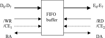
Figure 2.41 FIFO interface
If an SRAM is to be operated at high speed, the transfer of new addresses and control signals via the bus can be pipelined with the memory access to the previous one. The resulting structure using input registers for addresses and control signals is the synchronous SRAM. A memory bus equipped with an extra control signal (the clock) to signal the input events for addresses and read/write commands is called a synchronous bus. The synchronous burst SRAM (SBSRAM) chip is a common variant of the SRAM that integrates these registers and an increment function for the registered address as proposed above for the multiplexed bus (the use of SBSRAM on a synchronous multiplexed bus is non-standard). Some SBSRAM designs add additional registers for the write data and the read data.
There are a number of specialized memory architectures based on SRAM cells. If a second set of pass transistors and bus lines is added to an array of SRAM cells, one arrives at a structure providing two independent access ports to the memory that permit asynchronous accesses to the same storage cells via two separate buses. This structure is called a dual-port RAM (Figure 2.40). It is useful for implementing parallel read and write operations or for interfacing to subsystems without restricting the timing of their memory accesses. If a single port memory were used, they would have to compete for the right to access the memory data and address buses and would have to perform their accesses one-by-one. The dual-port RAM doubles the possible rate of read and write cycles (the ‘memory bandwidth’) and e.g. allows the pipelined inputting of new data into the memory without restricting the read accesses to previous data still stored in it. Dual port RAM modules packaged as chips suffer from the large number of interface signals to the two buses. The use of multiplexed buses helps this.
Another common memory structure that is also used to interface two subsystems and provides independent read and write ports is the first-in-first-out buffer (FIFO). The FIFO is a serial memory. A sequence of words can be input that are stored at subsequent locations, the addresses of which are generated automatically by integrated counters. The read operations retrieve the words one-by-one in the order in which they were input. A FIFO is usually equipped with extra logic to support synchronization by outputting handshaking signals BA and DA indicating the buffer space or read data being available (Figure 2.41). These interface definitions for the read and write ports are generic for handshaking input and output via the bus and can be adopted for many interfaces transmitting or receiving data streams. Other data structures like the last-in-first out buffer (LIFO or ‘stack’) with a single bus port yet without address lines can be implemented by combining the SRAM with appropriate address generator circuits that could otherwise also be computed by a sequential processor.
The associative, content addressable memory (CAM) can also be based on the SRAM cell. Its read operation performs a search for a word location holding a particular pattern that is input to the memory and outputs the address at which it is stored or other data associated to the input pattern. The CAM can be thought of as encoding the multi-bit search pattern by another (shorter) code. The write operation places a search key and an associated data pattern into a new location. CAM structures are used in cache memories (see section 6.2) where a portion of a large yet slow memory is mapped to a small, fast one, encoding the long addresses of the first by the short ones of the second. They also provide an efficient way of storing a large yet sparse, indexed data set (where most of the components are zero). Only the non-zero values are stored along with the indices. The CAM implements a computational function (the comparison) along with its storage cells.
While the SRAM storage cell is similar to a static D latch, the DRAM cell is like a dynamic D latch. The storage element in it is a tiny capacitor (a fraction of a pF) that keeps its voltage through time as long as it is not charged differently. A single pass transistor switch is used to connect the capacitors in a column to a common bus line, again using the structure shown in Figure 2.39 (where ‘M’ is now the capacitor). Thus, a single transistor per bit is required which explains the higher bit count of DRAM devices. A 256 M bit device hence contains about 256 million transistors and capacitors. Two problems arise. First, when the storage capacitor is switched to the extended bus line that has a much higher capacity, the stored charge is distributed to both capacitors and the voltage breaks down. The voltage on the bus line must consequently be amplified, and the full voltage must be restored to the cell capacitor (through the pass transistor). Secondly, for a non-selected cell the charge cannot be guaranteed to remain in the storage capacitor within the limits of the H and L levels for more than about 0.1s. Hence all rows of the memory must be periodically read out and rewritten independently from the access patterns of the application. This is called ‘refreshing’ the memory.
The row access to a DRAM takes some time to amplify and restore the data while the selection of a column position within the row is fast. This is exploited by applying the row and the column addresses sequentially on the same address inputs (thereby reducing the pin count) and by allowing fast ‘page mode’ accesses. One might expect a further multiplexing with the data, but this is not common. The access time from applying the row access may be about 40ns, while subsequent column accesses are 2–4 times faster. Figure 2.42 shows the timing of a page mode read cycle (for the write cycle it is similar). Several column addresses are applied in sequence and signaled by the /CAS transitions. The /RAS and /CAS control signals are typical to the DRAM. They substitute /CE on the SRAM and identify the input events for the row and column addresses.
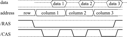
Figure 2.42 DRAM read cycle using multiple page accesses (data follow /CAS edges)
As in the case of SRAM, higher performance DRAM chips interface to a synchronous bus and include registers for the address and control inputs including /RAS and /CAS, for the data, and a counter function for the column address register to support accesses to subsequent locations without having to issue extra address latch commands. With these extensions the DRAM becomes the synchronous DRAM (SDRAM). Clock rates are in the range of 100..200 MHz, and sequential accesses can be performed at that rate. Still faster accesses are obtained by transferring data on every clock edge. The double data rate (DDR) SDRAM chips achieve this by using several banks on memory that are accessed in an interleaved fashion so that each individual block transfers data at a reduced rate. A typical DDR chip transfers stores 16 million 16-bit words and transfers them at a rate of up to 333 MHz (still much slower than the clock rate of some recent processors). A quad data rate SDRAM has been proposed using two interleaved DDR banks, the clocks of which are phase shifted by 90 degrees. The RAMBUS DRAM is a variant of the DRAM that pipelines the transfer of serialized commands and addresses to the data transfer using a smaller number of signal lines only. It achieves word transfer rates of up to 800 MHz on sequential transfers using both edges of a 400 MHz clock.
The application of an address in two halves to the DRAM that is usually generated as a single n-bit word, the generation of the /RAS and /CAS signals and the generation of refresh cycles require additional support circuits. The selection of the row to be refreshed is supported by an extra counter circuit integrated onto the DRAM chip, but the refresh cycles are not related to the application processing and must be interleaved with the read and write operations. The use of DRAM (in particular, SDRAM) is common for recent processor chips and some integrate the DRAM support circuits. If these are integrated onto the memory chip the interface signals may be made compatible to the generic bus interface of an SRAM. Chips of this kind are called pseudo-static. They combine the easy interface of an SRAM with the density of a DRAM.
The non-volatile Flash EPROM uses a single transistor cell with an extra fully isolated gate, the charge of which determines whether the transistor will conduct once it is selected by means of the main gate. Once charged, the isolated gate holds its charge infinitely and even during power off. The gates can be discharged electrically in large blocks and be charged selectively using the Tunnel effect. In the erased EPROM all storage cells output the H level, and programming a cell can only change an H to an L level. The erasure can only be applied to large blocks within the cell array (on the related EEPROM the cells can be erased individually). Erasing and programming require higher voltages and are fairly slow. Current flash memories include charge pumps to automatically generate them. The writing process is initiated by performing a series of special write operations with a timing similar to SRAM write operations that store the write data and address into registers, start the pump and trigger an internal circuit to control the subsequent charging of the isolated gates of the selected cell. The high voltage stresses the silicon structure, and the number of erase cycles is limited. Current chips support up to a million erasures, offer up to 64 M bit cells and guarantee a data retention time of 20 years. The read cycles are fairly fast (about 100 ns) and unlimited in their number.
The write cycles needed to initiate the programming of a cell mainly serve protect it against accidental writes due to software flaws or hardware-related faults. For a common 8-bit wide EPROM chip it is as follows (the data and address words are given in hexadecimal notation):
- Write $AA to address $5555.
- Write $55 to address $2AAA.
- Write $A0 to address $5555.
- Write data to desired address.
At the end read operations from the location just programmed reveal whether the programming of the location is terminated (this may take about 10ms). Several locations in the same row of the cell array may be programmed in parallel to reduce the total time. A similar sequence of write cycles is needed to perform the erase operation.
Often, the contents of an EPROM are copied into a faster memory during the startup phase of a system. For this block transfer, subsequent locations need to be selected by means of stepping through the address patterns. The address generation can be integrated into the EPROM chip to further simplify its interfacing. Actually the address patterns within the EPROM do not need to be related to the addresses appearing on the address bus of a processor reading its contents as long as the sequence of data words to be output is pre-determined. There are serial EPROM chips of this kind that output bit or byte sequences of up to 8 M bits and are housed in small packages with 8 to 28 pins. Their interface does not show any address signals but only a reset input for their internal address counter. For their programming, a serial protocol is used to enter the address and the write command.
As Flash EPROM chips are erased and programmed by means of electrical signals generated from the standard supply voltage, they can be attached (soldered) to a circuit board if the programming signals can be generated on it or routed to it via some interface. This is in contrast to former EPROM chips that required the exposure to ultraviolet light through a glass window in their package for their erasure, the application high programming voltages and special signal patterns. They were usually mounted in sockets and erased and programmed using special equipment.
Non-volatile storage at capacities of many G bytes but slower access times and strictly serial access schemes are the well-known rotating magnetic and optical storage devices (hard discs, DVD) which are interfaced to digital systems whenever long-term mass storage is required. Magnetic storage devices have been used since the early days of electronic computation.
A new generation of semiconductor memory chips is being developed (FRAM and MRAM) that rely on two competing cell technologies based on the ferro-electric and magneto-resistive effects. They promise non-volatile low-power storage combined with the high densities and the fast read and write operations found in current DRAM chips [22]. In 2001, the first commercial FRAM products appeared, including a 32k byte memory chip with the SRAM bus interface (see Figure 2.35) and operating at 3.3V, and by the end of 2002 a 64M bit chip was reported, and a 1 M bit MRAM, too.
2.2.3 Processors and Single-Chip Systems
The elementary Boolean gates with a few transistors only but individual inputs and outputs are not good candidates for a highly integrated standard chip without also integrating interconnection facilities (see section 2.2.4). If, however, a particular, complex Boolean function can be used in many applications (or in a system that is needed in very high volume), its integration makes sense. This is the case for the Boolean functions that implement the arithmetic operations on signed and unsigned binary numbers and floating point codes that are the building blocks in all numeric algorithms. If a complex function can be applied several times, one will try to reuse the same circuit with the aid of auxiliary select and control circuits. This gives rise to another important class of standard components or modules, the programmable processors.

Figure 2.43 Generic processor module interface

Figure 2.44 Single processor-based digital system (CE decoder not shown)
A processor chip integrates a multifunction circuit providing a number of complex Boolean functions (e.g., the arithmetic operations on 16-bit binary numbers) and a control circuit for the sequencing and the operand selection. In order to support many applications (each with its own sequence of operations and operand selections), it interfaces to a memory holding a list of operation codes (instructions) for the operations to be carried out. The same memory can also be used to store the operands. The interface to a generic processor chip or module is shown in Figure 2.43. It is complementary to the standard memory interface in Figure 2.35. The processor drives the address and control lines of the memory bus (to which a memory module is attached) to sequentially read instructions and operands and to write results. The bus can also be used to access input and output ports that are connected to it like memory chips using decoded chip enable signals. If the sequential execution of operations performed by the processor meets the performance requirements of an application, then the system can be as simple as shown in Figure 2.44.
The structure and the design of processors will be studied in much more detail in Chapters 4, 5, 6 and 8. The most important attributes of a processor are the set of Boolean functions provided by it (in particular, the word size of the arithmetic operations) and the speed at which they can be executed. Commercial processor chips range from processors integrating a few thousand transistors and providing some 8-bit binary arithmetic and some other Boolean operations on 8-bit codes at a rate of a few million operations per second (MOPS) to processors executing arithmetic operations on 64-bit floating point codes at rates beyond a giga operations per second (1 GOPS = 1000 MOPS) and employing more than 107 transistors.
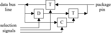
Figure 2.45 Configurable bit port with data (D) and control (C) flip-flops
The programmable processor and the memories to be interfaced to it are modules that instead of being realized as separate standard chips can also be integrated onto a single chip. Entire small systems of the type shown in Figure 2.44 are offered commercially as standard systems-on-a-chip (SOC) even including the inverter and PLL circuits for the clock oscillator and the Schmitt trigger circuit for the reset input. They are single-chip micro computers integrating e.g. a 16-bit processor, Flash EPROM, some SRAM, and a selection of standard interfaces including parallel and serial ports (except for the signal drivers) and counters (see section 6.6). On some recent chips the selection is quite abundant and for every specific application only a subset of the interfaces can actually be used. The unused others, however, do not draw current, and enable the chip to be used in more applications. The term SOC is also applied to systems realized on a single application-specific circuit (ASIC) or systems realized on a single FPGA (see below) and just reflects the fact that all of the design hierarchy becomes mapped to a single chip.
The interfaces implemented in a standard SOC product can usually be configured, to serve as many applications as possible. The pins of the chip package may e.g. be programmed to be input or output signals or to serve special purposes such as extending the on-chip memory bus. The control signals required to select the different hardware functions are generated by means of control registers that are connected to the on-chip bus and can be written to under software control. Figure 2.45 shows a single-bit port that can be configured as an input or as an output by means of a control flip-flop. A number of such single-bit ports can be connected in parallel to the data lines of the bus to provide the parallel input or output of binary words. Configuration registers are used for various other purposes such as to set the bit rates and the data formats of asynchronous serial interfaces, or to define the address range at which a chip select signal provided for some external memory or port device becomes active.
2.2.4 Configurable Logic, FPGA
The individual CMOS gates and registers that are needed as building-blocks of application-specific computational circuits are not suitable to be packed as integrated chips as this approach cannot exploit the current level of integration. Instead, it is large inventories of such building blocks that are offered as chips with a provision to connect them in an application-specific way within the chip.
Even if most of the functions within a digital system are within highly integrated chips, there may remain some auxiliary ‘glue logic’ to interface them with each other, to decode selection signals for chips connected to a bus, or for some extra control and interface signals. A common choice is to implement such functions (except for bus and interface drivers) in a single or a few PLD devices (programmable logic device). PLD devices arrived in the 1980s as a replacement for the large variety of gate and registers functions used in small-scale integrated circuits before. They are multifunction circuits in which the selection signals of the actual function are generated on-chip. In the first PLD generations, the selection was defined once and for all by burning fuses within the silicon structure. Now these are generated by EEPROM cells that can be reprogrammed several times. The configuration memory and the transistor switches of a PLD add to its complexity, and any particular application will only use a part of its gates and flip-flops. As the PLD functions are usually just a small fraction of the overall digital system, these overheads are outweighed by the advantages of the higher integration of application specific functions and the possibility to change the circuit functions to some degree without changing the board design. PLD devices are programmed with bit streams that are compiled from a set of Boolean equations defining the desired behavior by design tools.
More specifically, PLD devices contain identical slices, each generating a signal that is defined by OR'ing a few (e.g., 8) AND terms computed from the input and output signals of the device and their complements, i.e. a low complexity disjunctive form, and optionally outputting their complements, or a registered signal by providing an integrated flip-flop (Figure 2.46). Output pins may be tri-stated and also serve as inputs. The AND terms are realized as wired AND functions and selected by means of a matrix of transistor switches. These switches and the output selectors are controlled by an on-chip non-volatile, electrically erasable memory. Thus the same PLD device can be configured for various functions including registers, feedback circuits using registers, decoders and selectors.
PLD chips start from small packages of just 18 input and output signals. More complex ones include hundreds of flip-flops and provide many interface signals to accommodate application specific interfaces or systems functions such as DRAM control. They are usually composed of several simple PLD sub-modules that each selects a limited number of inputs from an interconnection structure spanning all of the chip. Some PLD circuits can be fixed to the circuit board and provide an interface that allows them to be programmed ‘in circuit’.
A complex PLD can be used for computational functions, too, but more flexibility and a still higher degree of integration of application-specific functions on configurable standard chips are provided by the field programmable gate arrays (FPGA). These allow for single chip implementations of complete digital systems and constitute a universal architecture for application specific design. An FPGA provides a large array of identical configurable cells. The configurable functions of these are the elementary building blocks of the FPGA architecture. A typical FPGA cell computes a 4-input Boolean function and also provides a flip-flop (Figure 2.47). Only the border cells are special and connect to the external interface signals of the FPGA package. The inputs to a cell are selected from the outputs of others according to the configuration data. They cannot be selected, however, from arbitrary outputs of the thousands of others but only from the direct neighbors of the cell and from a limited number of longer-distance wiring segments that can be linked to longer-distance connections if needed. The cells are arranged in a regular pattern and fill out the chip area. The regular arrangement of the cells and their fixed interconnection facilities permits the FPGA architecture to be scaled, i.e. to build larger arrays from the same kind of cells and to offer families of FPGA chips with cell arrays of different sizes. Current high-density FPGA devices offer more than 10000 cells and the equivalent of a million of gates (not counting the configuration memory and the switches). The number of border cells grows with the total size of the FPGA. Generally, FPGA packages have higher pin counts than memory chips, exceeding 1000 for the largest FPGA packages.

Figure 2.46 PLD slice feeding an output (simplified)

Figure 2.47 Generic FPGA cell
Most current FPGA devices use SRAM configuration memories. The configuration RAM can be automatically loaded with a sequence of bits or bytes from a serial Flash EPROM. Alternatively, the FPGA can be attached to a processor bus using an integrated control port and receive the sequence of configuration data words from there. The control port is attached to the data bus of the processor, and the processor reads the configuration words from its own EPROM which is hence shared by the processor program and FPGA data. The same control port can be used as an interface from the processor to the FPGA circuits after configuration.
The use of SRAM for the configuration memory implies the additional capability of reconfiguration for different steps of a computation which can raise the overall efficiency in some applications. The control port may include address lines to give the attached processor random access to the configuration memory. Then, the overheads involved in a serial configuration protocol are avoided, but at the expense of having to dedicate many interface signals of the FPGA to the purpose of configuration. Some FPGA chips also offer the capability of being partially reconfigured. Then a part of the application circuit is changed while the remaining circuits keep running. To exploit this, one has to set apart a subarray of the FPGA to which the changes are confined and to use fixed interfaces to the rest of the FPGA. Due to such restrictions, and without the support of high-level tools, partial reconfiguration is only rarely used. The large amount of configuration memory and the bit- or byte-serial access to it result in fairly long (re-)configuration times. Current FPGA chips do not provide an extra configuration memory that could be loaded in a pipelined fashion without interrupting the current configuration. Thus the reconfiguration time for an FPGA cannot be used for computations. The full or partial reconfiguration of an FPGA can exploit a control flow to use different configurations for the alternative branches of an algorithm (Figure 2.48).

Figure 2.48 FPGA reconfigure (R) and compute process (repetitive)
The loading of new blocks of configuration data is not directly supported by the automatic load circuits of the FPGA but requires an additional control circuit (that could be part of the serial EPROM device) or the loading by an attached processor. It is quite similar to loading new blocks of instructions into the internal instruction cache memory (see section 6.2.3) of a programmable processor, which is essential for running complex applications on it, too. Without an extra load circuit, an FPGA intended for SOC applications would have to support the reconfiguration control flow through some persistent application circuit and would therefore need the capability of partial reconfiguration.
FPGA chips suffer from large configuration overheads. For example, to configure an arbitrary Boolean function of four inputs, a 16-bit configuration memory used as a lookup table (LUT) is required. More is required for the input and output switches and for switches between wiring segments. Current FPGA devices consume 128–320 bits of configuration data per cell and accept a more than 10-fold overhead in chip area for their configurability (100-fold comparing to an optimized integration of the application circuit without building on multi-function cells). Moreover, due to the limited interconnection resources the available cells cannot be used all in a given application, and some of the cells are only used inefficiently. An efficient design reconfiguring the FPGA resources can use a smaller cell array and proportionally reduce the configuration overheads.
The performance of an FPGA implementation is lower than that of an equivalent fixed-configuration ASIC due to the larger size of the FPGA chip and the delays through the electronic switches. Similarly to ASIC designs, the timing of the application circuit is not the result of its structure (the ‘algorithm’) but depends heavily on the routing of the interconnections by the design tools. The resulting high cost by performance ratio of FPGA circuits is partially compensated by saving on the board level due to the higher integration and the fact that the FPGA is a standard part that can be produced in volume to serve many applications. Also, as long as the configuration data don't change, the configuration circuits inside the FPGA do not consume power. A common way to fight the low overall efficiency of FPGA devices is to integrate standard building blocks such as memory arrays, fixed multi-bit functions and even programmable processors into the devices. Processors integrated into the FPGA chip are useful for implementing the sequential control of FPGA circuits that is needed for the efficient usage of the cells (see section 1.5.3). Simple control circuits and even processors can also be built from the memory arrays and cells of the FPGA (see Chapters 5 and 6).
Apart from the processing speed of the cells and the level of integration resulting from the underlying chip technology, the available FPGA architectures differ in such basic features as the capabilities of the cells, the definition of the neighborhood of a cell and the provided pattern of wiring segments, and the choice and integration of predefined standard structures, and such system-related features as their input and output capabilities and features related to their configuration or the handling of clock signals. While the memory chips of the different categories (SRAM, DRAM, etc.) have similar structures and are easily compared by their parameters, the design of an FPGA architecture leaves many choices. All are concerned with the efficient usage of cells for arithmetic operations and make sure that basic arithmetic circuit elements like the binary full adder with a product operand (see section 4.1) can be realized in a single cell, and provide memory blocks for banks of registers and sequential control that cannot be realized as efficiently with the cell flip-flops. Some play tricks to make certain configuration circuits available for the application processing. To compare different FPGA architectures, one has to determine the total cost and the performance obtained in particular, relevant applications (the results of such analysis also depend on the quality of the tools generating the configuration code).
Although the FPGA is provided as a basis of application specific design, it is interesting to consider the task of designing an FPGA architecture as well which includes a proper choice of building blocks and a versatile interconnection structure. Following the above remarks and those made in section 1.5.3 the configuration overheads can be reduced by doing the following:
- Keeping the set of configurable cell functions small;
- Using fairly complex functions;
- Sharing configuration circuitry between several cells;
- Providing predefined structures for sequential control;
- Supporting pipelined partial reconfiguration loads.
FPGA structures with complex cells have been considered in the research literature [23]. A simple approach to sharing control is to perform identical functions on sets of two or four cells or to use a more complex cell like the one proposed in section 4.4, and to switch segments of multiple wires, which slightly increases the overall costs if just the single bit operations can be used but significantly reduces the configuration overhead otherwise. The dependencies of the timing and the correct function of application circuits on the routing could be dealt with by a two-level scheme distinguishing local (fast) connections between cells and long-distance connections routed through switches and wire segments and using handshaking for the latter. An FPGA architecture suitable for asynchronous circuits was reported on in [24]. Finally, one would consider integrating a control circuit to perform multiple reconfigurations (or even multiple threads of partial reconfigurations). In the commercial FPGA products only the integration of some complex predefined functions has been realized. Some integrate simple processors that can also be used to perform reconfigurations of the FPGA. The following examples show the different feature mixes in some of the current products.
The At40k family from Atmel provides a range of low-to-medium density FPGA devices that operate from a single 3.3V supply. These devices may not cover entire systems but are convenient for application-specific interfaces and special functions. The largest one, the At40k40, contains an array of 48 × 48 cells (i.e., 2304), each providing a Boolean function of four inputs (or two functions of three inputs) and a flip-flop. The ‘40’ suffix refers to a claimed equivalent of about 40000 gates (about 18 per cell). The other FPGA manufacturers’ families make similar claims with even higher ratios of gates per cell. Although a look-up table of 16 entries does require 15 select gates, these numbers are misleading. It is more useful to compare the number of 4-bit look-up tables. Real applications implement special Boolean functions and never expoit the complexity of the cells as a universal circuits, and hardly pack more than a full adder plus AND gate (the multiplier building block) into an average cell, which is the equivalent of 6 gates.
The At40k cells receive input from their 8 neighbors and interface to 5 vertical and 5 horizontal bus lines that span 4 cells each and can be connected to adjacent wire segments through extra switches. For every group of 4 × 4 cells there is an extra 32 × 4 bit dual port RAM block that can e.g. be used to implement banks of registers or simple automata. The RAM blocks can be combined into larger RAM structures. The border cells can be configured for different load currents. A typical package is the 20 × 20 mm2 144-pin TQFP. There are about 128 configuration bits per cell (including those used by the switching network). The At40k FPGA chips receive their configuration data from a serial EPROM or via an 8- or 16-bit data port controlled by an external processor and can be partially reconfigured.
A important extension to the At40k family are the At94k devices that significantly enhance the FPGA resources by also integrating an SRAM of 16k 8-bit words (bytes) and an 8-bit processor with another 10k 16-bit words of SRAM to hold its instructions. The data SRAM is e.g. useful to implement data buffers for interfaces implemented in the FPGA that would otherwise need access to an external memory. The processor can be used in particular for the fast reconfiguration of parts of the FPGA circuits (even individual cells) through a fast, internal interface to the FPGA configuration memory, with the option to implement a control flow for a compute and reconfigure process of the FPGA (Figure 2.48). On the At40k an equivalent interface is available to an attached processor at the price of more than 32 dedicated FPGA signals, the corresponding amount of circuit board area, and the generation of wide addresses by the attached processor. On the At94k, no external FPGA signals are needed for this purpose, and the time-consuming reconfiguration does not have to be handled by some attached processor. The integrated processor can also be used for the sequential control of FPGA functions. Besides these FPGA enhancements, it can also be used for conventional software functions such as input and output via serial interfaces and real-time control using the integrated timers. The processor bus does not leave the chip; only some interfaces from the processor section are connected to package pins. The At94k devices are pin compatible to the At40k devices and loaded with configuration and program code from the same kind of serial memory via a three-wire interface. The combined hardware and software capabilities allow for numerous applications of the simple FPGA plus EPROM set-up.
The Virtex II family from Xilinx provides medium-to-high density devices with predefined arithmetic building blocks. The devices use a 1.5V supply for the cell array but support 3.3V for the pin drivers. As an example, the XC2V1000 device provides as many as 10240 cells with a 4-input LUT and a flip-flop each in a 17 × 17 mm2 256-pin BGA package or in a range of larger ones (less complex Virtex II chips starting from 512 cells are available in the 256-pin package, too). The cells are grouped by 8 into 1280 configurable logic blocks (CLB). Inside a CLB the look-up tables can be combined, and some extra gates speed up the binary add. Each CLB is connected to a switch matrix (SM) that implements the switched connections to the adjacent and more distant ones (Figure 2.49). Each matrix has double connections to each of the eight neighboring matrices, multiple connections to the horizontal and vertical neighbors at distances 2, 4, 3 and 6, to horizontal and vertical long lines spanning the entire chip and to four horizontal bus lines, and can pass an input signal to an output without switching it to the attached CLB. Bus lines are supported, too. The cells within the CLB are coupled more tightly so that two levels of interconnections may be distinguished (in contrast to the Atmel architecture). There are about 300 configuration bits per cell. The XC2CV1000 is a multi-million transistor chip.
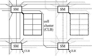
Figure 2.49 Interconnection structure of the Virtex-II FPGA
As a special feature of the Virtex architecture, the 16-bit LUT defining the Boolean function performed by a single cell can be changed into a 16-bit dual port RAM or a 16-bit shift register by reclaiming configuration resources for the application circuits. The XC2V1000 also provides 40 dual port RAM blocks of 18k bit each (a total of 90k bytes). Moreover, there are 40 predefined arithmetic building blocks performing the multiplication of 18-bit signed binary numbers with a 36-bit result. They are interfaced to the RAM blocks and are most suitable in signal processing applications where many multiplications can be carried out in parallel. The implementation of an 18-bit parallel multiplier by means of cells would cost at least 324 cells (see section 4.3), the 40 multipliers hence 12960 cells. The multiplier building blocks are much smaller and faster than the equivalent cell networks and have no configuration overheads. The Virtex-II FPGA also provides a testing interface through which configuration data can be loaded and read back. It also supports partial reconfiguration and provides access to the contents of the flip-flops and memory locations. Moreover, it can also be used as a serial interface from within the application. Finally, there are sophisticated resources for the generation and synchronization of clock signals, and various options for the signal levels at the pins including LVDS. Serial interfaces built with these achieve bit rates of up to 840 Mbit/s.
The Virtex-II family has been extended to the Virtex-II Pro family that also includes programmable processor modules (up to 4) based on the PowerPC architecture (see section 6.6.4) and still faster serial interfaces including special shift registers and encoding clock and data on the same lines. The processor modules are fast 32-bit processors executing up to 400 million instructions per second (MIPS) at a power consumption of less than 0.4W and each include 32k bytes of cache memory. They are optionally interfaced to the FPGA memory blocks. More memory would be added by interfacing memory chips to some pins of the FPGA chip and by routing the processor bus to these. It may be useful to dispose of several sequential control circuits, but the PowerPC modules appear oversized for just controlling FPGA circuits and would typically take over a substantial part of the application processing. They do not have access to the configuration memory.
The APEX family from Altera also extends to high densities. The smallest packages are 484 pin 22 × 22 mm2 BGA packages. The EP20k1000 e.g. provides as many as 38400 cells with a 4-input lookup table and a flip-flop in each in a 672-pin package. The cells come in logic array blocks of 10 (LAB) which are the counterparts of the Virtex CLBs. 24 blocks line up into a ‘mega lab’ which is a subsystem supplying local connections to neighboring LABs and a set of extra connections between all of them. 160 mega labs are attached to a grid of horizontal and vertical ‘lanes’ across the chip. Each mega lab also contains an embedded system block (ESB) that can be configured to provide PLD style logic functions, i.e. disjunctive forms with more input variables than supported by the LUT cells, or serve as a 2k bit dual port RAM. As a special feature of the APEX architecture the ESB can be configured to operate as a 1k bit CAM memory. The APEX device uses about 224 configuration bits per cell (including the bits for the routing). Altera also offers the APEX chip with an integrated 32-bit ARM processor running at 200 MIPS (section 6.6.3), and also additional SRAM for it. The ARM processor can be used to (totally) reconfigure the FPGA cell array and to implement a control flow for the reconfigurations. The smallest version integrates 32k bytes of processor memory and an interface to external SDRAM memory and yields a complete FPGA plus processor system if a single 8-bit wide Flash EPROM chip is added. A memory bus to external DRAM chips is useful in many FPGA applications. Although the processor plus memory part occupies much less chip area than the FPGA part, the chip does not seem to be conceived as an FPGA enhancement but more as a single chip system also integrating the common sequential processor component to implement software functions.
A more recent architecture from Altera is the Stratix family. It provides larger memories (yet no longer the CAM option) and arithmetic building blocks. The chip EP1S25 with 25660 cells includes a total of about 256k bytes including two large dual port RAM blocks of 72k bytes each. It also contains 40 18-bit multipliers and associated adders that are grouped into 10 digital signal processing (DSP) blocks. The multipliers in a DSP block can also be configured to perform eight 9-bit or a single 36-bit binary multiplication. The Stratix devices also implement LVDS and include fast shift registers. 8-bit multipliers are also provided on a recent FPGA from Quicklogic.
While the Virtex II and Stratix families are expensive high-end products that are intended as platforms to implement entire high-performance application-specific systems including the required computational functions, there are lower-cost derivatives from them in cheaper packages such as a 144-pin TQFP with or without a smaller number of special arithmetic functions and with smaller amounts of integrated RAM that still extend to considerable densities. They support LVDS interface signals and can be used to implement fast serial interfaces using the FPGA cells and are typically used to implement interface functions to other processors although they also permit the implementation of simple processors and systems. These new, lower-cost FPGA families let the FPGA become attractive in a broader range of low-to-medium volume applications. These include simple processor and software-based applications as the available cell counts suffice for the implementation of simple processors.
The low-cost version derived from the Virtex II architecture is the 1.2V Spartan-III family. This is the first FPGA to be fabricated in a 0.09 μ technology. It shares many features of the VirtexII but is slightly slower and provides a lower density for the multipliers and the embedded RAM. The XC3S400 device is the densest one offered in the 144-pin TQFP (which we fix as a parameter related to the board level costs). It packs about 8000 cells, 32k bytes of RAM and 16 multipliers, and maintains the special Xilinx feature of being able to use some cells as 16-bit registers. The low-cost variant of Stratix is the 1.5V Cyclone FPGA. The EP1C6 packs nearly 6000 cells and 10k bytes of RAM into the same package. Both families achieve high clock rates and fast arithmetic functions through dedicated carry signals. An FPGA with a similar density but using an integrated Flash memory instead of an SRAM to hold the configuration data and which consequently needs no extra storage device to become operational is in the ProASIC+family from Actel. The At94k40 FPGA is comparable to these more recent FPGA chips in terms of cell count and RAM integration. These latter achieve better cost to complexity ratios, higher clock rates and new interfacing options yet do not provide the special reconfiguration and processor support of the At94k.
Table 2.1 Evaluation of some FPGA chips

Source: Compiled by W. Brandt, TU Hamburg-Harburg
Table 2.1 lists the estimated clock rates and cell counts achieved for these chips in two reference designs using a common vendor independent tool (except for Spartan III), using a global clock for all registers. The first is a 32-bit processor core with the MIPS I architecture [48], and the second uses a behavioral definition of an early version of the CPU2 (see section 6.3.2) without any structural optimizations. Note that an overview of this kind just represents a snapshot of some current chip offerings at a particular time. The results of a particular reference design do not necessarily carry over to other designs and also depend on the optimization capabilities of the design tools and the suitability of the design to the particular FPGA architecture. The specific predefined functional blocks (e.g. memory blocks) of an FPGA architecture require some changes in a processor design. A general rule is that the cost to performance ratio offered by an FPGA family is mostly related to the feature size of the technology used for it (this also holds for processor chips). The most recent offerings simply outperform the older ones but they may lack particular features such as partial reconfiguration. The high number of cells needed for the Actel FPGA reflects its simpler cell structure. Note that there is no Atmel device with 5000+ cells. The actual clock rates for the designs depend on the results of the placement and routing steps (cf. section 7.5). For a Virtex II FPGA, estimated clock rates are about 30% slower. After placement and routing they get reduced by about another 30% for the MIPS design, but remain close to the estimate for the other. For both, the cell counts decrease. The supplied data are thus fairly incomplete and only clearly indicate the difficulties of benchmarking.
2.3 CHIP LEVEL AND CIRCUIT BOARD-LEVEL DESIGN
Circuit boards are used to mount the individual hardware building blocks (chips and others), to interconnect them, and to provide access to the interface signals via connectors. They also distribute the power and participate in removing the heat generated by the components. Larger digital systems are realized by several circuit boards mounted on ‘motherboards’ or in racks and cabinets. The circuit board simply constitutes the next hierarchical level of the hardware. As for the pin count of chips, it is desirable to have low signal counts at the external interfaces of a circuit board (the connectors). The design of the circuit boards can be so that they can easily be plugged together by means of connectors, or be performed by mapping several design modules to a single board. The main difference between the design levels of chip, board and cabinet design are in the degree of miniaturization and reliability and in the cost involved in designing application-specific systems and building them in a given volume. In contrast to the integrated circuits, boards are more expensive but easier to design, rely on a simpler manufacturing technology and can be used to implement low volume applications at reasonable costs. Still simpler yet more costly technology is required if an application-specific system can be plugged together from existing boards. If, however, the volume goes higher, it is more cost effective to map several boards to a single one, and multiple components to a single ASIC.
The design choices for a circuit board are similar to the ones for chip design. As in the case of the chips, a circuit board is a fixed, invariable hardware module. A circuit board design can be made so that different subsets of components can be supported and different components match with a compatible interface. The fixed hardware structure of a circuit board can be compensated by designing it to be configurable. Then it may allow more than one application or changes within an application without having to redesign the board. A standard circuit board serving many applications can be produced in higher volume (at lower cost), and its development costs become shared. Also the module interfaces at the chip and board levels are similar. It is e.g. common to link several boards via bus lines.
The interconnection of the chips is by fine leads on the surface of an epoxy carrier plane etched out from a copper coating. Circuit boards use between 1 and 12 interconnection planes fixed on top of each other. Leads at different planes are connected via connections (‘vias’) chemically deposited in small holes through the layers. It is common to use dedicated non-etched layers for the ground and power supply voltages. The integrated circuits are mounted to the top and bottom surfaces of the board. The placement of the components and the routing of the interconnection through the layers are done with the aid of CAD tools (as in the case if chip design; for very simple boards, they can be done manually).
For the electrical design issues of circuit boards we refer to [2] and [9] except for a few remarks. The power supply noise caused by synchronous clock transition at many sites overlays all digital signals and must be taken care of by connecting the power planes through capacitors with low series resistances. On a circuit board the digital signals may change at rates of up to several 100 MHz (on-chip rates even extend to several GHz). Traces on the circuit board beyond a few cm must be considered as wave guides at the ends of which reflections may occur that overlay the digital signal, and in some cases cause a faulty operation of the high-speed digital circuits interfaced to it. Therefore such signal lines need to be driven through series resistors matched to the impedance of the transmission line (typically 24…100Ω) and, at longer distances or for bus lines, to be terminated at the ends by a matched resistive load. The signal delays at longer distances need to be considered, and synchronous signals such as the clock and the data lines of a synchronous serial bus should be routed close to each other (this is even true for long-distance connections within a chip). A signal travels 15-20 cm in a time of 1ns. There may be cross-talk between signal lines, and high frequency signals are radiated so that the digital system may have to be shielded in order to keep this radiation within required limits. Cross-talk and radiation are low for differential signals such as those according to the LVDS norm. In mixed analog/digital systems even a slight cross-talk from the fairly large digital signals (in particular, clock signals and power supply signals) to the involved analog signals can be a severe problem. Usually, the analog circuits such as operational amplifiers are set apart from the digital ones and get an extra ground reference that is linked to the digital ground at a unique site only, and an extra, decoupled power supply line.
2.3.1 Chip Versus Board-Level Design
It is possible to trade off chips level integration for board level integration to minimize the total cost. A circuit board can be collapsed into a single chip, but sometimes it can be more cost effective not to use a highly integrated chip but to distribute its functions to several chips (higher volume ones, or chips from different vendors).
The manufacturing costs of the circuit boards grow with the board area, with the number of layers, and the number of vias between the layers. For a simple board design, the integrated circuits should have as simple interfaces as possible (in terms of the number of i/o signals). This requirement is, of coarse, common to all modular structures (including software modules). For a single chip system the board design becomes almost trivial as, apart from simple support functions, only the external interface signals must be routed from the chip to appropriate connectors. System designs of this kind arise when a single-chip micro controller with integrated memory suffices to fulfill the processing requirements, or an FPGA configured from a serial EPROM.
This simplicity is not always achieved. If e.g. a processor chip needs a large external memory, a large number of interfacing signals is required. Current highly integrated chips have hundreds of interface signals. High pin counts require BGA packages that can no longer be supported by single or double layer circuit boards at all and hence raise the cost of the circuit board design even if just a subset of them is used for an application. An exception to the board costs increasing with the pin counts of the chips occurs when the layout of the pins of two chips to be connected to each other is so that they can be arranged side by side and the connections become short and are within a single board layer.
Wide memory buses and multiple signal lines not only consume board area but also cause capacitive loads and signal delays. In contrast, multiple, wide memory structures can be easily supported within a medium-sized chip. For large chips, propagation delays, capacitive loads and the wiring area are an issue, too, although less than at the board level. Extended buses with multiple (capacitive) loads, in particular buses extending to several boards, require the buffering of the local signals with auxiliary driver circuits, and maybe partitioning into several segments. Buffering and partitioning cause additional signal delays. There is thus an advantage in not extending a bus outside a board, and in attaching a small number of circuits only mounted at a small distance. The highest performance results if the bus signal does not need to leave the chip at all.
Some techniques to simplify the chip interfaces and thereby the circuit boards have already been discussed. One is to use multiplexed buses if off-chip buses are required at all. The other is to use serial interfaces instead of parallel ones if the required data rate allows for this. A serial bus designed to connect a number of peripheral circuits to a processor is the I2C bus introduced by Philips. It uses two open collector signal bus lines only pulled up by resistors (one for the data and one for a clock signal) and supports data rates of up to 400k bits/sec. As a bus it is shared for the data exchanges with all the different attached peripherals, and the data rate is shared as well. Every device connected to the I2C bus has an address that is transferred via the bus, too, to direct subsequent data to it. The I2C bus significantly simplifies the board design yet at the cost that the processor and every peripheral chip need to implement the serial interface and the address decoding required for selecting between them (Figure 2.50). Simple I2C peripherals have addresses that are predefined up to one or two bits which are defined by wiring some device pins to H or L. An I2C bus is a multi-master bus that may be shared between several processors used in a system. It provides a mechanism to detect collisions due to simultaneous attempts to output to the bus. Serial interfaces used to simplify the wiring of chips within circuit boards can also be based on LVDS interfaces that operate at much higher data rates.

Figure 2.50 Serial interface bus with attached interface modules

Figure 2.51 Processor board design (case study)
The same techniques apply to arrive at simple board-level interfaces. If no bus extended beyond the board, no bus drivers and connectors are required and the high frequency signals that may be used by the on-board circuit do not appear outside. Serial interfaces between the boards reduce the wiring effort. If only external i/o and network interfaces remain, the boards become cheaper and simpler.
As a case study we present a general purpose circuit board design from standard components announced or available in 2003 (Figure 2.51). As a general purpose board it should provide useful computational resources as characterized in terms of kinds and numbers of available operations per second, configurable input and output interfaces, and some networking interfaces for multi-board applications in order to be applicable as an architectural component. Moreover, the board design might allow for different selections of components in order to efficiently support different classes of applications. Intended applications for the board were its use within a large distributed control and measurement system, and its use to control an autonomous robot vehicle. Requirements from these applications were the availability of an Ethernet interface (section 6.5.3.3) and support for the TCP/IP protocols, a CAN bus interface (section 6.5.3.1), an asynchronous serial interface, several counter and timer functions, and a particular, small size. The manufacturing costs of the board should be kept low by not using BGA packages that would require more than four circuit layers. The non-volatile memories should be programmable without removing them from the board.
Some standard chip offerings integrate several of the required system components in a convenient way. One could have used an integrated processor including the Ethernet support and the CAN bus like the Motorola MCF5282, or a floating point processor like the SH7750 (see section 6.6.4). There is a choice of fairly powerful micro controllers for automotive applications packing a CAN controller, counter and timer functions, analog input, and even the required program memory, e.g. the XC161 from Infineon, the DSP56F8356 from Motorola, or the TMS320F2812 from Texas Instruments (section 6.6.2). Instead, it was decided to place the costly Ethernet interface, the CAN bus controller and the number crunching support onto separate chips that would only be mounted if required. The networking of several boards and general purpose, configurable interfaces including the required counter and timer interfaces would be supported by an FPGA. A fast micro controller with DSP capabilities (the Blackfin processor, see section 8.4.3) is provided to supply computational resources for the application programs and for the IP protocol support, using a separate serial Flash memory chip as its program store and to hold the code for the other devices. Separate flash memory chips are offered with higher capacities and endurances than inside the integrated processors. If analog input is needed (cf. section 8.1.1) a separate ADC chip can deliver a better performance as well.
The Blackfin chip integrates some SRAM and controls an optional SDRAM chip. Its integrated PLL clock generator allows the operating speed of the board and its power consumption to be adjusted to the needs of the applications. The LAN controller chip interfacing the board to the Ethernet is connected to the micro controller via the FPGA chip. It also integrates extra buffer space for the Ethernet frames and was selected to support the 100 Mbit rate as many boards may have to share the Ethernet bus. The FPGA is a Spartan III chip that provides fast serial interfaces for connecting several boards using LVDS signals and can also be used as an additional compute circuit. The micro controller can be used to reconfigure the FPGA. The optional coprocessor provided for applications that need fast floating point processing is an integrated DSP chip (see section 8.5) operating in parallel to the micro controller using an on-chip instruction and data memory of 256k bytes of its own. It also adds some extra interfaces. The processors provide up to about 109 16-bit integer or 32-bit floating point operations per second at a power consumption of about 1W. If just the Blackfin and the Flash memory chips are used, the power dissipation becomes as low as 0.2W.
The size of this fairly powerful processor board is only about 10 × 10 cm (there are just 5 larger chips including the LAN controller), and it uses just four layers (2 signal and 2 power supply layers) which is the result of keeping the interfaces between the chips at a strict minimum. The only chip requiring a large number of interface signals to a processor bus is the optional SDRAM chip. The segmentation of the bus through the FPGA simplifies the wiring and allows both segments to be used independently. The processing functions could have been packed even more densely by using BGA packages yet at the expense of higher board manufacturing costs. The chips all interface via 3.3 V signals and only need an additional 1.2V core voltage supply which is due to the consistent use of chip technologies. The board holds the needed switching regulator to generate it and runs from a single voltage supply. Various interface signals leave the board, but no bus leaves it for a further memory expansion. The Flash memory can be programmed by connecting a USB adapter to the board.
2.3.2 IP-Based Design
In a board level design one selects components such as processor, memory, and interface chips and connects them on the board according to their bus interfaces. Similarly, in an ASIC or an FPGA based SOC design one also tries to compose the desired function from proven modules of similar kinds. A common module such as a processor is a standard structure that requires additional software tools for its programming and some specific know-how on its capabilities, their interfacing and the related design tools. Then, it is desirable to use such a component in many designs.
As well as reusing components developed in previous designs, it has become common to licence standard components called IP modules (intellectual property modules) and the related tools in very much the same way as one previously did for chips at the board level from vendors specialized in providing well-tested component designs with a guaranteed performance and the tool support. IP modules may be offered for specific FPGA families and without access to the component design apart from its interface, or as portable sources in some hardware design language that allow the component to be synthesized on several platforms. In contrast to hardware components (chips) IP modules may be parameterized, allowing e.g. the word size of a generic processor architecture and the number of registers actually implemented to be adjusted to the cost and performance requirements of an application. In some cases, however, the licensing conditions for IP modules may exclude their use in small volume applications.
Xilinx and Altera both offer processor cores for the FPGA families discussed in section 2.2.4. The 16/32-bit NIOS processor core from Altera e.g. can be used for the APEX, Stratix and Cyclone devices and is supported by a C compiler. A processor realized with the costly resources of an FPGA must achieve a sufficient performance using as few FPGA cells as possible, and interface through some simple software and hardware interface to FPGA memory blocks, companion IP modules, and application specific FPGA circuits. NIOS uses about 1000 cells of an APEX device and achieves a performance of 50 MIPS. The system-on-a-chip design based on a set of IP modules can be supported by software tools composing a component and interconnection table from a menu-driven user interface. The SOC builder tool from Altera lets one specify the processor and memory parameters, and the numbers and kinds of certain serial and parallel interfaces than then become synthesized on the FPGA. Several NIOS processors can be implemented and interfaced to each other on an FPGA. The bus of a processor implemented on an FPGA or an ASIC constitutes an important module interface for IP modules from other vendors or for the integration of application-specific interfaces to the processor subsystem. On-chip bidirectional data buses are not always available. Then the bus specifies separate read and write signal sets and selector circuits to connect the data output of some device to the read data lines of the processor. Examples are the Avalon bus used for the NIOS processor or the high-performance bus specified in the advanced microcontroller bus architecture (AMBA) for ARM processor based systems [45].
2.3.3 Configurable Boards and Interconnections
The ability to configure a board for different applications results from the use of configurable components on it, e.g. an EPROM chip to hold different programs, and interfaces controlled by configuration registers that are written to by a processor with data from the EPROM. Other configuration inputs may simply be set the L or H level by means of miniature make switches or jumpers plugged onto configuration connectors.
The connections within a board including those to the external interface connectors may be routed via such switches, too, to support alternative configurations. The mechanical components can be avoided through the use of electronic switches controlled by configuration registers (similar to those within FPGA devices). Then the board design becomes simpler, and the dynamic reconfiguration of the hardware resources becomes possible. An interface signal of the circuit board may e.g. be routed to several destinations, or be generated from a choice of circuits. The electronic switching can be supported by special integrated circuits (‘crossbars’) providing switches between a number of i/o signals that are controlled by memory cells. The crossbar function can also be implemented on an FPGA, or simply by routing the connections to be configured through an FPGA device.
Configurable interconnections can be used to implement the through routing of an input signal to an output signal without being processed on the board. A faulty board can e.g. be bypassed or substituted by a spare one. Then multiple boards can be mounted and wired in a fixed arrangement (e.g. using a motherboard) and still use application-specific interconnections. The basic FPGA structure of an array of configurable components connected via a network of electronic switches is thus generalized and ported to the board level to yield system architectures with interesting properties.
As a case study we consider the ER2 parallel computer architecture [25]. The ER2 is a scalable board-level configurable system that is similar to an FPGA structure in several respects. Like an FPGA it is a general purpose system that can be used for a variety of applications. The ER2 builds on just three board level components, an electronically controlled crossbar switch, a compute module that can be attached to the crossbar, and a motherboard for a number of crossbar switches that are interconnected on it in a grid structure, each switch being connected to four neighboring ones or to connectors at the border of the motherboard. The motherboards can be plugged together via edge connectors to form larger networks. The crossbars are connected to their neighbors via multiple wire segments (24 wires in the east and west, 18 in the north and south directions, see Figure 2.52). The switch boards are small circuit boards (X) containing the crossbar circuit, a control processor with RAM and EPROM memories and an FPGA chip implementing a set of auxiliary pre-configured interfaces to the neighbors. The configuration of the switches for an application is performed by the control processors that receive the application-specific control data through the auxiliary interfaces. The program code for the processors is also distributed that way. The control processors can also be used for the application processing. The main compute resource, however, is the compute module (C) that interfaces to a switch module via 6 fast serial interfaces each using 6 wires and by an interface port to the control processor of the switch. It contains a cluster of four tightly coupled processors of the Sharc family (see section 8.5.1).

Figure 2.52 Configurable interconnection network with attached compute modules
The board components of the ER2 allow digital systems of arbitrary size to be composed without involving additional electronic design. The prototype system shown and described in [55] includes 256 crossbars and 64 processor clusters. The crossbar network would support other kinds and mixes of different kinds of compute modules as well. The crossbar sites not connected to a compute module contribute to the routing resources and can be used for input and output interfaces, or to provide extra connections between different crossbars. The grid interconnection on the motherboards is just the basis of an application-specific wiring of the compute modules which can even be changed during a computation or be used to implement rerouting capabilities to spare boards. The scalability of the architecture results from the strictly local interconnection structure. Each switch added to the system to provide a new compute site also adds to the interconnection resources. In contrast, conventional standard processor boards connecting to a shared memory bus as offered by many manufacturers only allow for a small number of processor boards in a system.
The overall architecture of the ER2 is similar to an FPGA architecture using complex, programmable processors operating asynchronously for the cells, and multi-bit serial transfers via the connections using handshaking. The algorithms placing the application functions to the processors and routing interconnections are similar to FPGA place and route algorithms, too. A processor cluster is comparable to the CLB in Figure 2.49. In contrast to the FPGA that only provides input and output to the border cells, the board level architecture has the important advantage of allowing it at every compute module. The different clusters operate asynchronously and the interfaces connecting them through the switches perform handshaking to at least synchronize for the data exchange.
The crossbar circuit used in the ER2 design is the IQ160 from the I-Cube family of switches that has meanwhile disappeared from the market. It provides 160 i/o signals which can be configured as inputs, buffered outputs and as bi-directional signals. In the bi-directional mode an i/o signal also runs through a buffer circuit but without requiring a direction control signal to select between input and output. It is held at the high level by a pull-up resistor and becomes input if a high-to-low transition is initiated externally and output if it is initiated internally. Due to the buffering a signal passing the crossbar undergoes a small delay (about 10ns). The inputs and outputs can optionally be latched in on-chip input and output registers.
The local control of the crossbars makes the reconfiguration of the network a distributed task of the set of control processors. It is, however, simple to just change the connection from an interface of the attached compute module to a crossbar to another signal connected to the crossbar on the motherboard and thereby to use the same interface at different times for different interconnection paths. Also it is possible to select between several local interfaces to communicate along a switched path through the network. The compute module also provides some lower speed serial interfaces that require just two signals. These can be switched through the crossbars, too. The crossbars can be thought of as a configurable interface of various local interfaces to the wiring media on the motherboards. The aspect of reserving an application-specific amount of the communications bandwidth provided by the media is also used in other interfacing schemes (e.g. the USB, see section 6.5.3.2).

Figure 2.53 Versatile module interface using a crossbar
The idea of using a scalable network of crossbars as the interconnection media of scalable digital systems can be applied in many variants using different processor building blocks, implementing crossbars on FPGA chips and using other crossbar interconnection schemes and balances between the compute and the crossbar modules. The ER2 architecture can e.g. be moved to the chip level to provide single-chip configurable processor networks [26, 27], which will be further discussed in Chapter 7. As the cells are complex processors, the control overheads of the fine-grained FPGA architectures are avoided. By integrating a crossbar function with some handshaking support, almost every single-chip system or circuit board with a single or few processors and interfaces can be equipped with a module interface that supports the multiplexing and through-routing capabilities needed to use it as a component in a scalable architecture (Figure 2.53).
2.3.4 Testing
In order to be able to detect manufacturing (and design) flaws, it is necessary to provide testing facilities for every digital system. This is done by feeding the system with test input data and by verifying that the outputs obtained with these are correct. If the system, as usual, is constructed from modules, the testing is applied at the level of the modules to find out whether they operate correctly before it is applied to the structure composed by them.
As the interfaces to the modules are not required for the application processing, it requires an extra design effort to give access to them. To independently test a module one needs to be able to switch a source of test data to its inputs and to select its output signal. Actually the testing of the individual module does not depend on its wiring within the system. For a chip, the access to its subcircuits is in conflict with the requirement of a simple module interface (pin count). The test signals are applied to chip sites not connected to regular package pins, or shared with package pins, or to serial interfaces provided to support testing with as little extra signals as possible.
At the board level one needs to verify that the chips mounted to the circuit board and already tested after manufacturing are connected correctly. The wires connecting them are not easily accessible. They are packed quite densely, connect to the chips beneath the package and can even be routed in the middle layer of the board only. The solution to this testing problem is to integrate switches onto the chips that disconnect the internal signals from the pins, connect test inputs and outputs instead, and give access to these by means of a special serial interface (Figure 2.54).
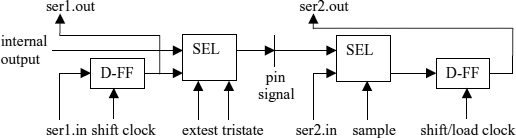
Figure 2.54 Boundary scan circuit for a package pin

Figure 2.55 JTAG chain
There is an industry standard for the design of this interface called JTAG (joint test action group)[28]. It defines an interface of five test signal inputs and outputs, namely:
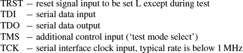
and a set of commands that are serially input using these signals into an instruction register of at least two bits if a particular pattern is chosen for TMS. Otherwise the data shift register is selected (with a register bit for every signal to be tested), or a bypass flip-flop. The TRST signal is not always implemented as the reset state can also be obtained by inputting a special bit pattern on TMS. The most important commands are:

The command set can be expanded by commands specific to the chip, e.g. to access special registers of a processor used for the software debugging in a single step mode, or to use the JTAG pins for a general purpose serial interface for application data (Xilinx).
As there are several chips within a system, the JTAG signals are chained (Figure 2.55) to give serial access to all of them via a single test interface. Data bits are input to TDI with the rising edge of TCK, and the TDO event is with the falling edge. The instruction and data registers of the chips in the chain are put in series. A typical sequence of commands is to shift in the test data pattern and then the EXTEST command to all chips of the chain, then to issue the SAMPLE command for the inputs and to output them via TDO to the test equipment. This is repeated with varying test patterns until all connections have been verified. BYPASS is used to selectively input to or output from a particular chip in the chain only.
According to Figure 2.54 the JTAG interface needs a shift register bit and selectors for every signal to be tested, the command and bypass registers and the TMS control. Usually it is only implemented for complex integrated circuits where it represents just a small fraction of the overall hardware. For the inputs and output from a board or sub-circuits within it, there are multi-bit driver circuits equipped with a JTAG interface.
On a circuit board with a processor equipped with the JTAG interface and an SRAM or EPROM memory attached to its bus, the test mode can be used to drive the bus lines to test the memory by verifying its functions (even if it does not have a JTAG port of its own). This is also a common way to perform the in-circuit programming of a Flash EPROM. JTAG accesses are slow due to the serial interfacing and cannot be used to track the signal changes of a running system (in ‘real time’). Some chips also use the JTAG interface to scan internal signals at the interfaces between chip modules that are not accessible at all otherwise, or use the interface to provide extra debugging functions through special commands.
2.4 SUMMARY
In this chapter we explained the CMOS circuit and chip technology that is mostly used to build digital systems. The CMOS technology provides the basic Boolean gate function and storage elements that can easily be composed to almost any degree of complexity. The power dissipation of CMOS circuits has been discussed, including methods such as clock gating, asynchronous and adiabatic logic to reduce it. The digital design proceeds from the CMOS circuit level in a hierarchical fashion to more complex building blocks, the highly integrated chips and to circuit boards, with emphasis on reusing proven modules as standard components, and on extending their scope by making them configurable. The design of chips and circuit boards turns out to be quite analogous. Configurability and programmability at the board level and for interconnecting boards are as useful as they are for chips. Coarse-grained FPGA like architectures with (re-)configurable interconnections can cover many applications with a small inventory of components. Chip designs proceed similarly to board level designs, namely by combining proven, complex modules (IP modules) such as processors, memories and interfaces that might show up as chips in an equivalent board level design but now are components of a system-on-a-chip. Both at the chip and at the board levels more distant system components need to provide simpler interfaces. Ideally, on a large chip or board, distant subsystems are interfaced serially using a few signal lines only and operate asynchronously.
EXERCISES
- Boolean functions implementing binary arithmetic often build on the full adder function that calculates from three inputs X,Y,Z the outputs:

‘⊕’ denotes the XOR operation. Determine the gate counts for an implementations based on NAND, NOR and NOT gates, as a complex CMOS gate, and as a dual n-channel network gate with complementary outputs.
- Design a circuit realizing the MRS flip-flop from gates and from CMOS switches.
- Design a circuit generating bipolar handshake signals (with every transition defining an event, not just L-H) and the control signal for a data latch.
- Design a circuit having two clock inputs R and S and an output that is set to H by the L-to-H transitions on S and reset to L by the L-to-H transitions on R.
- Design a digital phase comparator for a PLL clock generator.
- Use an SRAM to design a LIFO stack that is accessed like a single register. Use registers to pipeline the SRAM access to the read or write operations.
- A ring counter is an automaton using an n-bit state register that cycles through the states 1000… 00,0100… 00,0010… 00,0001… 00, …, 0000… 10,0000… 01. Design the feedback circuit for it from elementary gates so that any initial state eventually transitions into the state 1000..00.
- Design a k-bit automaton with a single bit input that calculates the k-bit CRC code of a sequence presented at the input defined by a given mod(2) polynomial of degree k (see section 1.1.2).
- Design an address decoder circuit computing three chip select outputs from a 16-bit address input. CE1 shall be L for addresses in the range 0… 0x7fff, CE2 in the range 0x8000… 0x80ff and CE3 for the remaining addresses.
- Show that for every n-bit input k to the fractional n-bit frequency divider the most significant output bit changes with a mean rate of f*|k|/2n where f is the input frequency and |k| is the absolute value of k as a signed binary number. Derive an expression for the current consumption due to charging and discharging the adder inputs and the output.