15
Tensor Processing Unit
This chapter introduces the Tensor Processing Unit (TPU), a special chip developed at Google for ultra-fast execution of neural network mathematical operations. As with Graphics Processing Units (GPUs), the idea here is to have a special processor focusing only on very fast matrix operations, with no support for all the other operations normally supported by Central Processing Units (CPUs). However, the additional improvement with TPUs is to remove from the chip any hardware support for graphics operations normally present in GPUs (rasterization, texture mapping, frame buffer operations, and so on). Think of a TPU as a special purpose co-processor specialized for deep learning, being focused on matrix or tensor operations. In this chapter, we will compare CPUs and GPUs with the four generations of TPUs and with Edge TPUs. All these accelerators are available as of April 2022. The chapter will include code examples of using TPUs.
In this chapter, you will learn the following:
- C/G/T processing units
- Four generations of TPUs and Edge TPUs
- TPU performance
- How to use TPUs with Colab
So with that, let’s begin.
C/G/T processing units
In this section we discuss CPUs, GPUs, and TPUs. Before discussing TPUs, it will be useful for us to review CPUs and GPUs.
CPUs and GPUs
You are probably somewhat familiar with the concept of a CPU, a general-purpose chip sitting in each computer, tablet, and smartphone. CPUs are in charge of all of the computations: from logical controls, to arithmetic, to register operations, to operations with memory, and many others. CPUs are subject to the well-known Moore’s law [1], which states that the number of transistors in a dense integrated circuit doubles about every two years.
Many people believe that we are currently in an era where this trend cannot be sustained for long, and indeed it has already declined during the past decade. Therefore, we need some additional technology if we want to support the demand for faster and faster computation to process the ever-growing amount of data that is available out there.
One improvement came from GPUs, special-purpose chips that are perfect for fast graphics operations such as matrix multiplication, rasterization, frame-buffer manipulation, texture mapping, and many others. In addition to computer graphics where matrix multiplications are applied to pixels of images, GPUs turned out to be a great match for deep learning. This is a funny story of serendipity (serendipity is the occurrence and development of events by chance in a happy or beneficial way) – a great example of technology created for one goal and then being met with staggering success in a domain completely unrelated to the one it was originally envisioned for.
TPUs
One problem encountered in using GPUs for deep learning is that these chips are made for graphics and gaming, not only for fast matrix computations. This would of course be the case, given that the G in GPU stands for Graphics! GPUs led to unbelievable improvements in deep learning but, in the case of tensor operations for neural networks, large parts of the chip are not used at all. For deep learning, there is no need for rasterization, no need for frame-buffer manipulation, and no need for texture mapping. The only thing that is necessary is a very efficient way to compute matrix and tensor operations. It should be no surprise that GPUs are not necessarily the ideal solution for deep learning, since CPUs and GPUs were designed long before deep learning became successful.
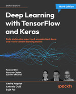
Before going into technical details, let’s first discuss the fascinating genesis of Tensor Processing Unit version 1, or TPU v1. In 2013, Jeff Dean, the Chief of the Brain Division at Google, estimated (see Figure 15.1) that if all the people owning a mobile phone were talking in calls for only 3 minutes more per day, then Google would have needed two or three times more servers to process this data. This would have been an unaffordable case of success-disaster, i.e., where great success has led to problems that cannot be properly managed. It was clear that neither CPUs nor GPUs were a suitable solution. So, Google decided that they needed something completely new – something that would allow a 10x growth in performance with no significant cost increase. That’s how TPU v1 was born! What is impressive is that it took only 15 months from initial design to production. You can find more details about this story in Jouppi et al., 2014 [3], where a detailed report about different inference workloads seen at Google in 2013 is also reported:
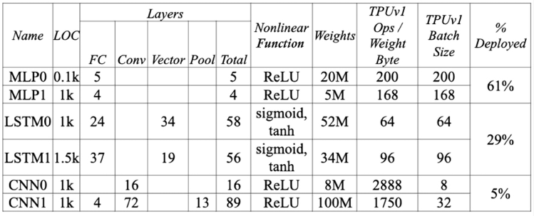
Figure 15.1: Different inference workloads seen at Google in 2013 (source [3])
Let’s talk a bit about the technical details. A TPU v1 is a special device (or an Application-Specific Integrated Circuit, or ASIC for short) designed for super-efficient tensor operations. TPUs follow the philosophy less is more. This philosophy has an important consequence: TPUs do not have all the graphic components that are needed for GPUs. Because of this, they are both very efficient from an energy consumption perspective, and frequently much faster than GPUs. So far, there have been four generations of TPUs. Let’s review them.
Four generations of TPUs, plus Edge TPU
As discussed, TPUs are domain-specific processors expressly optimized for matrix operations. Now, you might remember that the basic operation of matrix multiplication is a dot product between a line from one matrix and a column from the other matrix. For instance, given a matrix multiplication ![]() , computing Y[i, 0] is:
, computing Y[i, 0] is:

The sequential implementation of this operation is time-consuming for large matrices. A brute-force computation has a time complexity of O(n3) for n x n matrices so it’s not feasible for running large computations.
First generation TPU
The first generation TPU (TPU v1) was announced in May 2016 at Google I/O. TPU v1 [1] supports matrix multiplication using 8-bit arithmetic. TPU v1 is specialized for deep learning inference but it does not work for training. For training there is a need to perform floating-point operations, as discussed in the following paragraphs.
A key function of TPU is the “systolic” matrix multiplication. Let’s see what this means. Remember that the core of deep learning is a core product ![]() , where, for instance, the basic operation to compute Y[i, 0] is:
, where, for instance, the basic operation to compute Y[i, 0] is:

“Systolic” matrix multiplication allows multiple Y[i, j] values to be computed in parallel. Data flows in a coordinated manner and, indeed, in medicine the term “systolic” refers to heart contractions and how blood flows rhythmically in our veins. Here systolic refers to the data flow that pulses inside the TPU. It can be proven that a systolic multiplication algorithm is less expensive than the brute-force one [2]. A TPU v1 has a Matrix Multiply Unit (MMU) running systolic multiplications on 256 x 256 cores so that 65,536 multiplications can be computed in parallel in one single shot. In addition, a TPU v1 sits in a rack and it is not directly accessible. Instead, a CPU acts as the host controlling data transfer and sending commands to the TPU for performing tensor multiplications, for computing convolutions, and for applying activation functions. The CPU ![]() TPU v1 communication happens via a standard PCIe 3.0 bus. From this perspective, a TPU v1 is closer in spirit to a Floating-Point Unit (FPU) coprocessor than it is to a GPU. However, a TPU v1 has the ability to run whole inference models to reduce dependence on the host CPU. Figure 15.2 represents TPU v1, as shown in [3]. As you see in the figure, the processing unit is connected via a PCI port, and it fetches weights via a standard DDR4 DRAM chip. Multiplication happens within the MMU with systolic processing. Activation functions are then applied to the results. The MMU and the unified buffer for activations take up a lot of space. There is an area where the activation functions are computed.
TPU v1 communication happens via a standard PCIe 3.0 bus. From this perspective, a TPU v1 is closer in spirit to a Floating-Point Unit (FPU) coprocessor than it is to a GPU. However, a TPU v1 has the ability to run whole inference models to reduce dependence on the host CPU. Figure 15.2 represents TPU v1, as shown in [3]. As you see in the figure, the processing unit is connected via a PCI port, and it fetches weights via a standard DDR4 DRAM chip. Multiplication happens within the MMU with systolic processing. Activation functions are then applied to the results. The MMU and the unified buffer for activations take up a lot of space. There is an area where the activation functions are computed.
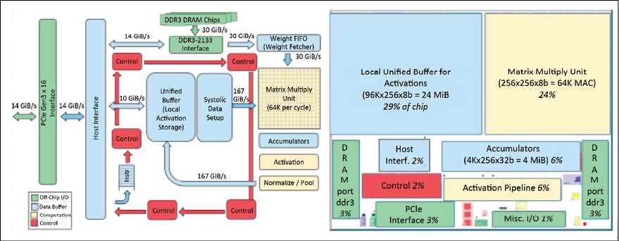
Figure 15.2: TPU v1 design schema (source [3])
TPU v1s are manufactured on a 28 nm process node with a die size of ≤ 331 mm2, a clock speed of 700 MHz, 28 MiB of on-chip memory, 4 MiB of 32-bit accumulators, and a 256 x 256 systolic array of 8-bit multipliers. For this reason, we can get 700 MHz*65,536 (multipliers) ![]() 92 Tera operations/sec. This is an amazing performance for matrix multiplications; Figure 15.3 shows the TPU circuit board and flow of data for the systolic matrix multiplication performed by the MMU. In addition, TPU v1 has an 8 GiB of dual-channel 2133 MHz DDR3 SDRAM offering 34 GB/s of bandwidth. The external memory is standard, and it is used to store and fetch the weights used during the inference. Notice also that TPU v1 has a thermal design power of 28–40 watts, which is certainly low consumption compared to GPUs and CPUs. Moreover, TPU v1s are normally mounted in a PCI slot used for SATA disks so they do not require any modification in the host server [3]. Up to four cards can be mounted on each server. Figure 15.3 shows a TPU v1 card and the process of systolic computation:
92 Tera operations/sec. This is an amazing performance for matrix multiplications; Figure 15.3 shows the TPU circuit board and flow of data for the systolic matrix multiplication performed by the MMU. In addition, TPU v1 has an 8 GiB of dual-channel 2133 MHz DDR3 SDRAM offering 34 GB/s of bandwidth. The external memory is standard, and it is used to store and fetch the weights used during the inference. Notice also that TPU v1 has a thermal design power of 28–40 watts, which is certainly low consumption compared to GPUs and CPUs. Moreover, TPU v1s are normally mounted in a PCI slot used for SATA disks so they do not require any modification in the host server [3]. Up to four cards can be mounted on each server. Figure 15.3 shows a TPU v1 card and the process of systolic computation:
Figure 15.3: On the left you can see a TPU v1 board, and on the right an example of how the data is processed during the systolic computation
If you want to have a look at TPU performance compared to GPUs and CPUs, you can refer to [3] and see (in a log-log scale graph) that the performance is two orders of magnitude higher than a Tesla K80 GPU. The graph shows a “rooftop” performance, which is growing until the point where it reaches the peak and then it is constant.
The higher the roof, the better performance is:
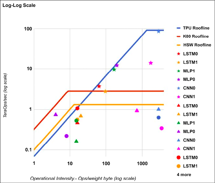
Figure 15.4: TPU v1 peak performance can be up to 3x higher than a Tesla K80
Second generation TPU
The second generation TPUs (TPU2s) were announced in 2017. In this case, the memory bandwidth is increased to 600 GB/s and performance reaches 45 TFLOPS. Four TPU2s are arranged in a module with 180 TFLOPS of performance. Then 64 modules are grouped into a pod with 11.5 PFLOPS of performance. TPU2s adopt floating-point arithmetic and therefore they are suitable for both training and inference.
A TPU2 has an MNU for matrix multiplications of 128*128 cores and a Vector Processing Unit (VPU) for all other tasks such as applying activations etc. The VPU handles float32 and int32 computations. The MXU on the other hand operates in a mixed precision 16–32 bit floating-point format.
Each TPU v2 chip has two cores, and up to four chips are mounted on each board. In TPU v2, Google adopted a new floating-point model called bfloat16 The idea is to sacrifice some resolution but still be very good for deep learning. This reduction in resolution allows us to improve the performance of the TPU2s, which are more power-efficient than the v1s. Indeed, It can be proven that a smaller mantissa helps reduce the physical silicon area and multiplier power. Therefore, the bfloat16 uses the same standard IEEE 754 single-precision floating-point format, but it truncates the mantissa field from 23 bits to just 7 bits.
Preserving the exponent bits allows the format to keep the same range as the 32-bit single precision. This allows for relatively simpler conversion between the two data types:
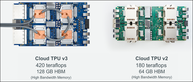
Figure 15.5: Cloud TPU v2 and Cloud TPU v3
Google offers access to these TPU v2 and TPU v3 via Google Compute Engine (GCE), and via Google Kubernetes Engine (GKE). Plus, it is possible to use them for free via Colab.
Third generation TPU
The third generation TPUs (TPU3) were announced in 2018 [4]. TPU3s are 2x faster than TPU2 and they are grouped in 4x larger pods. In total, this is an 8x performance increase. Cloud TPU v3 Pods can deliver more than 100 petaflops of computing power. On the other hand, Cloud TPU v2 Pods released in alpha in 2018 can achieve 11.5 petaflops – another impressive improvement. As of 2019, both TPU2 and TPU3 are in production at different prices:

Figure 15.6: Google announced TPU v2 and v3 Pods in beta at the Google I/O 2019
A TPU v3 board has four TPU chips, eight cores, and liquid cooling. Google has adopted ultra-high-speed interconnect hardware derived from supercomputer technology for connecting thousands of TPUs with very low latency.
Each time a parameter is updated on a single TPU, all the others are informed via a reduce-all algorithm typically adopted for parallel computation. So, you can think about a TPU v3 as one of the fastest supercomputers available today for matrix and tensor operations, with thousands of TPUs inside it.
Fourth generation TPUs
Google’s fourth generation TPU ASIC has more than double the matrix multiplication TFLOPs of TPU v3, a considerable boost in memory bandwidth, and more advances in interconnect technology. Each TPU v4 chip provides more than 2x the compute power of a TPU v3 chip – up to 275 peak TFLOPS. Each TPU v4 Pod delivers 1.1 exaflops/s of peak performance. Google claims that TPU v4 Pods are used extensively to develop research breakthroughs such as MUM and LaMDA, and improve core products such as Search, Assistant, and Translate (see https://blog.google/technology/developers/io21-helpful-google/). As of April 2022, TPU v4s are only available in preview (Figure 15.7):

Figure 15.7: A TPU v4 chip and a portion of a TPU v4 Pod – source: https://twitter.com/google/status/1394785686683783170
In this section, we have introduced four generations of TPUs. Before concluding, I wanted to mention that it is possible to save money by using preemptible Cloud TPUs for fault-tolerant machine learning workloads. These workloads include but are not limited to long training runs with checkpointing or batch prediction on large datasets.
Edge TPU
In addition to the three generations of TPUs already discussed, in 2018 Google announced a special generation of TPUs running on the edge. This TPU is particularly appropriate for the Internet of Things (IoT) and for supporting TensorFlow Lite on mobile and IoT. An individual Edge TPU can perform 4 trillion (fixed-point) operations per second (4 TOPS), using only 2 watts of power. An Edge TPU is designed for small, low-power devices and is ideal for on-device ML, with it being fast and power-efficient. Edge TPUs support the TensorFlow Lite development framework (see Figure 15.8). At the end of 2019, Google announced the Pixel 4 smartphone containing an Edge TPU called the Pixel Neural Core:
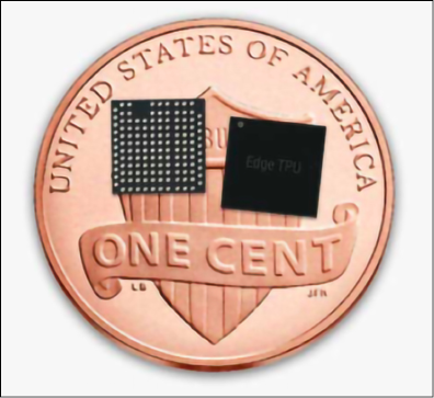
Figure 15.8: Two Edge TPUs on one penny – source: https://coral.ai/docs/edgetpu/faq/#what-is-the-edge-tpu
With this we conclude the introduction to TPU v1, v2, v3, v4, and Edge TPU. In the next section we will briefly discuss performance.
TPU performance
Discussing performance is always difficult because it is important to first define the metrics that we are going to measure, and the set of workloads that we are going to use as benchmarks. For instance, Google reported an impressive linear scaling for TPU v2 used with ResNet-50 [4] (see Figure 15.9 and Figure 15.10):
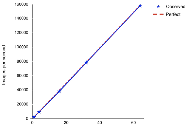
Figure 15.9: Linear scalability in the number of TPUs v2 when increasing the number of images
In addition, you can find online a comparison of ResNet-50 [4] where a full Cloud TPU v2 Pod is >200x faster than a V100 NVIDIA Tesla GPU for ResNet-50 training:

Figure 15.10: A full Cloud TPU v2 Pod is >200x faster than a V100 NVIDIA Tesla GPU for training a ResNet-50 model
According to Google, TPU v4 givse top-line results for MLPerf1.0 [5] when compared with Nvidia A100 GPUs (see Figure 15.11). Indeed, these accelerators are designed by keeping in mind the latest large models encompassing billions and sometimes trillions of parameters (think about GPT-3, T5, and the Switch Transformer):

Figure 15.11: MLPerf 1.0 TPU v4 Pod performance – source: https://cloud.google.com/blog/products/ai-machine-learning/google-wins-mlperf-benchmarks-with-tpu-v4
How to use TPUs with Colab
In this section, we show how to use TPUs with Colab. Just point your browser to https://colab.research.google.com/ and change the runtime from the Runtime menu as shown in Figure 15.12. First, you’ll need to enable TPUs for the notebook, then navigate to Edit→Notebook settings and select TPU from the Hardware accelerator drop-down box:
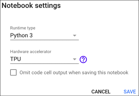
Figure 15.12: Setting TPU as the hardware accelerator
Checking whether TPUs are available
First of all, let’s check if there is a TPU available, by using this simple code fragment that returns the IP address assigned to the TPU. Communication between the CPU and TPU happens via gRPC (gRPC Remote Procedure Call), which is a modern, open-source, high-performance Remote Procedure Call (RPC) framework that can run in any environment:
%tensorflow_version 2.x
import tensorflow as tf
print("Tensorflow version " + tf.__version__)
try:
  tpu = tf.distribute.cluster_resolver.TPUClusterResolver()  # TPU detection
  print('Running on TPU ', tpu.cluster_spec().as_dict()['worker'])
except ValueError:
  raise BaseException('ERROR: Not connected to a TPU runtime; please see the previous cell in this notebook for instructions!')
tf.config.experimental_connect_to_cluster(tpu)
tf.tpu.experimental.initialize_tpu_system(tpu)
tpu_strategy = tf.distribute.experimental.TPUStrategy(tpu)
You should see something like the following:
Tensorflow version 2.8.0
Running on TPU  ['10.36.66.50:8470']
INFO:tensorflow:Deallocate tpu buffers before initializing tpu system.
INFO:tensorflow:Deallocate tpu buffers before initializing tpu system.
INFO:tensorflow:Initializing the TPU system: grpc://10.36.66.50:8470
INFO:tensorflow:Initializing the TPU system: grpc://10.36.66.50:8470
INFO:tensorflow:Finished initializing TPU system.
INFO:tensorflow:Finished initializing TPU system.
WARNING:absl:'tf.distribute.experimental.TPUStrategy' is deprecated, please use  the non experimental symbol 'tf.distribute.TPUStrategy' instead.
INFO:tensorflow:Found TPU system:
INFO:tensorflow:Found TPU system:
INFO:tensorflow:*** Num TPU Cores: 8
INFO:tensorflow:*** Num TPU Cores: 8
INFO:tensorflow:*** Num TPU Workers: 1
INFO:tensorflow:*** Num TPU Workers: 1
INFO:tensorflow:*** Num TPU Cores Per Worker: 8
INFO:tensorflow:*** Num TPU Cores Per Worker: 8
We’ve confirmed that a TPU is available!
Keras MNIST TPU end-to-end training
Referring to the notebook available on Google Research Colab (see https://colab.research.google.com/github/GoogleCloudPlatform/training-data-analyst/blob/master/courses/fast-and-lean-data-science/01_MNIST_TPU_Keras.ipynb#scrollTo=Hd5zB1G7Y9-7), we can check how TPUs or GPUs are detected with this code snippet, which uses either TPUs or GPUs as a fallback:
try: # detect TPUs
    tpu = tf.distribute.cluster_resolver.TPUClusterResolver.connect() # TPU detection
    strategy = tf.distribute.TPUStrategy(tpu)
except ValueError: # detect GPUs
    strategy = tf.distribute.MirroredStrategy() # for GPU or multi-GPU machines
    #strategy = tf.distribute.get_strategy() # default strategy that works on CPU and single GPU
    #strategy = tf.distribute.experimental.MultiWorkerMirroredStrategy() # for clusters of multi-GPU machines
print("Number of accelerators: ", strategy.num_replicas_in_sync)
Note that the strategy tf.distribute.TPUStrategy(tpu) is the only change you need in code for synchronous training on TPUs and TPU Pods. Then, to run TF2 programs on TPUs, you can either use .compile or .fit APIs in tf.keras with TPUStrategy.
If you want you can write your own customized training loop by calling strategy.run directly (see https://www.tensorflow.org/api_docs/python/tf/distribute/TPUStrategy).
Using pretrained TPU models
Google offers a collection of models pretrained with TPUs available in the GitHub tensorflow/tpu repository (https://github.com/tensorflow/tpu). Models include image recognition, object detection, low-resource models, machine translation and language models, speech recognition, and image generation. Whenever it is possible, my suggestion is to start with a pretrained model [6], and then fine-tune it or apply some form of transfer learning. As of April 2022, the following models are available:
|
Image Recognition, Segmentation, and More |
Machine Translation and Language Models |
Speech Recognition |
Image Generation |
|
Image Recognition AmoebaNet-D ResNet-50/101/152/2000 Inception v2/v3/v4 Object Detection RetinaNet Mask R-CNN Image Segmentation Mask R-CNN DeepLab RetinaNet Low-Resource Models MnasNet MobileNet SqueezeNet |
Machine Translation (transformer based) Sentiment Analysis (transformer based) Question Answer BERT |
ASR Transformer |
Image Transformer DCGAN GAN |
Table 15.1: State-of-the-art collection of models pretrained with TPUs available on GitHub
The best way to play with the repository is to clone it on the Google Cloud console and use the environment available at https://github.com/tensorflow/tpu/blob/master/README.md. You should be able to browse what is shown in Figure 15.13:
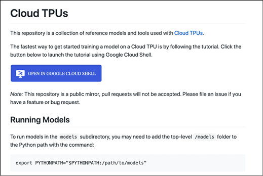
Figure 15.13: Cloud TPUs
If you click the button OPEN IN GOOGLE CLOUD SHELL, then the system will clone the Git repository into your cloud shell and then open the shell (see Figure 15.14):
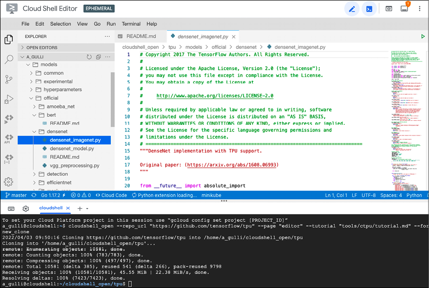
Figure 15.14: Google Cloud Shell with the TPU Git repository cloned on your behalf
From there, you can play with a nice Google Cloud TPU demo for training a ResNet-50 on MNIST with a TPU flock – a Compute Engine VM and Cloud TPU pair (see Figure 15.15):
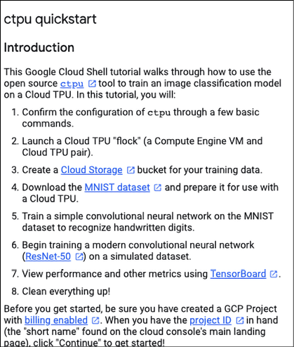
Figure 15.15: Google Cloud TPU demo for training a ResNet-50 on MNIST with a TPU flock
I will leave this training demo for you if you are interested in looking it up.
Summary
TPUs are very special ASIC chips developed at Google for executing neural network mathematical operations in an ultra-fast manner. The core of the computation is a systolic multiplier that computes multiple dot products (row * column) in parallel, thus accelerating the computation of basic deep learning operations. Think of a TPU as a special-purpose co-processor for deep learning that is focused on matrix or tensor operations. Google has announced four generations of TPUs so far, plus an additional Edge TPU for IoT. Cloud TPU v1 is a PCI-based specialized co-processor, with 92 teraops and inference only. Cloud TPU v2 achieves 180 teraflops and it supports training and inference. Cloud TPU v2 Pods released in alpha in 2018 can achieve 11.5 petaflops. Cloud TPU v3 achieves 420 teraflops with both training and inference support. Cloud TPU v3 Pods can deliver more than 100 petaflops of computing power. Each TPU v4 chip provides more than 2x the compute power of a TPU v3 chip – up to 275 peak TFLOPS. Each TPU v4 Pod delivers 1.1 exaflops/s of peak performance.
That’s a world-class supercomputer for tensor operations!
In the next chapter, we will see some other useful deep learning libraries.
References
- Moore’s law: https://en.wikipedia.org/wiki/Moore%27s_law
- Milovanović, I. Ž. et al. (May 2010). Forty-three ways of systolic matrix multiplication. Article in International Journal of Computer Mathematics 87(6):1264–1276.
- Jouppi, N. P. et al. (June 2014). In-Datacenter Performance Analysis of a Tensor Processing Unit. 44th International Symposium on Computer Architecture (ISCA).
- Google TPU v2 performance: https://storage.googleapis.com/nexttpu/index.html
- MLPerf site: https://mlperf.org/
- A collection of models pretrained with TPU: https://cloud.google.com/tpu
Join our book’s Discord space
Join our Discord community to meet like-minded people and learn alongside more than 2000 members at: https://packt.link/keras
