
CHAPTER 7 Larger Systems and the PIC 16F873A
Over the previous five chapters the PIC 16F84A has been used as the example microcontroller. It, and other microcontrollers like it, are fine devices for the smaller product. However, there are many things they cannot do, and for more demanding applications we need to look to a more powerful microcontroller. But what does ‘more powerful’ actually mean? Remember what was said in Chapter 1, that a microcontroller is essentially made up of:
Microprocessor core plus memory plus peripherals
More ‘power’ can be added to a microcontroller by enhancing any of these areas. The core, containing the CPU, can be made more powerful by making it faster or enhancing the internal architecture or instruction set. The memory can be made ‘more powerful’ by updating its technology or increasing its capacity and speed. Alternatively, or in addition, more peripherals can be added or the current peripherals enhanced.
In many cases in embedded systems, the most dramatic advance is not made by enhancing the core. Instead, it is the addition of new peripherals, perhaps accompanied by memory upgrades, which give the main sense of progress. With the addition of appropriate peripherals, suddenly analog-to-digital conversion, serial communication, or complex timing functions, become readily available.
In this section of the book, Chapters 7–12, we stay with the PIC 16 Series. We move, however, from a small member of the family to larger ones, mainly the PIC 16F873A. As the 16F84A and 16F873A are both members of the same family, the core and instruction set remain constant, but the ability to engage in embedded control is dramatically enhanced by the addition of an excellent range of ‘new’ peripherals. In the last chapter of the section we look at potential upgrade paths for both the 16F84A and 16F873A.
In these chapters the material is illustrated by application to the Derbot Autonomous Guided Vehicle (AGV). If you are not building a Derbot, don't worry; it will still act as a perfect case study for introducing the many new concepts that we will meet. We remain with Assembler programming, but will begin to experience the limitations both of using Assembler and of some of the hardware features of the 16 Series. This will lead in a logical way to the final section of the book, where we take on the challenge of an advanced microcontroller, programming in C, and the development of complex, multi-tasking programs.
As we move to larger systems, it is important to develop greater ability to get them working and to get them working reliably. Therefore, this chapter introduces new and important diagnostic tools and techniques, which are applied in the chapters that follow.
By the end of the chapter, you should have a good grasp of:
• The architecture of the 16F87XA family, of which the 16F873A is a member.
• Some of the more advanced tools used for the testing and commission of an embedded system.
If you are building the Derbot AGV, this chapter will also give you guidance on the first step of a staged construction, which will continue over several chapters.
7.1 The main idea – the PIC 16F87XA
The 16F873A, our example microcontroller, is part of a family group that was briefly introduced at the beginning of Chapter 2. The group is made up of the 16F873A, the 16F874A, the 16F876A and the 16F877A. Generically, we can refer to them as 16F87XA. Each microcontroller in the group also has an LF version, for example 16LF873A, which can run at a lower power supply voltage than the standard device.
The features of this group are summarised in Table 2.1. Looking back at that table, it is easy to see that the four group members are distinguished simply by different memory sizes and different package sizes, whereas the larger package allows more parallel input/output ports to be used. This is illustrated in the pin connection diagrams of Figure 7.1. The ‘extra’ pins on the larger devices are enclosed in a dotted line. It can be seen that a primary difference is the Port D and Port E that the ’874A and ’877A have.

Figure 7.1 The PIC 16F87XA pin connection diagrams. (a) 16F873A/876A. (b) 16F874A/877A (‘extra’ pins enclosed in dotted boxes)
The descriptions that follow in this chapter, and in all chapters up to 11, tend to use the 16F873A as the example device, as this is used in the Derbot AGV project that we will study. The other members of the group are, however, mentioned at times, particularly if they have a feature not found in the ’873A.
7.2 The 16F873A block diagram and CPU
The block diagrams of both the 16F873A and the ’876A are shown in Figure 7.2. The difference between the two microcontrollers lies in memory size, as detailed in the table at the bottom of the diagram. It is worth studying this diagram carefully and comparing it in detail with the 16F84A block diagram of Figure 2.2. This will show that there are some areas that are identical, others where there has been slight incremental change, others where the diagram is effectively the same but has been drawn in a different way, and others where there are a large number of additions.
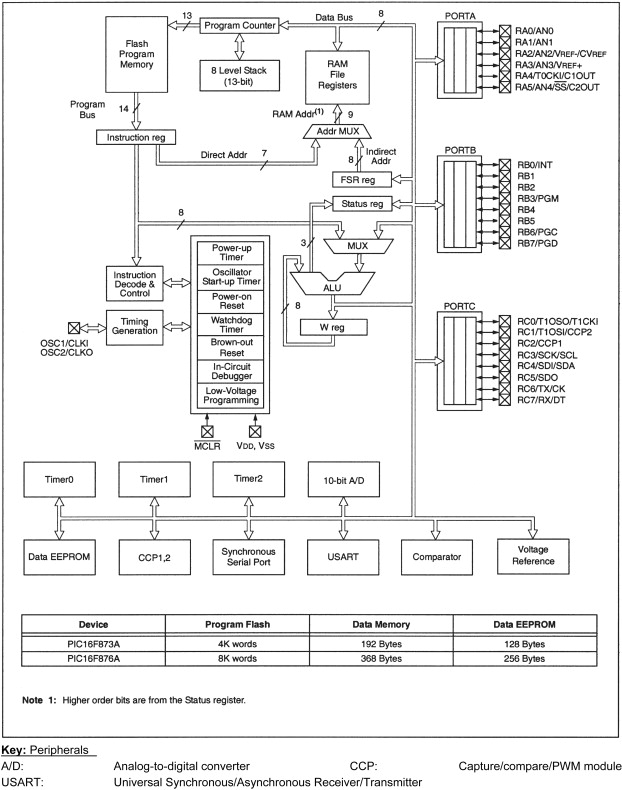
7.2.1 Overview of the Central Processing Unit and core
Let us note first that the CPU structure, made up essentially of the ALU, Working register and Status register, remains, as expected, like the ’F84A. The addition in this diagram of three lines from the ALU to the Status register is simply an acknowledgement of the three status bits in the Status register, Z, DC and C, which are controlled from the ALU. The lines could be included in Figure 2.2.
One difference that does occur in the CPU is in the Status register. With the 16F84A Status register (Figure 2.3), the upper two bits are not used, while bit 5 is used to select between the two banks of data memory. Figure 7.3 shows the Status register for the 16F87XA. With its much bigger data memory, the higher three bits of the Status register are now all used for memory bank selection. Apart from this, the Status register remains unchanged.

7.2.2 Overview of memory
Further to the CPU being similar to the 16F84A, it is easy to see that the whole memory structure is also the same, with some slight adjustments. The 13 program address lines from the Program Counter, which can address 213 (i.e. 8192) memory locations, are now fully exploited in the 16F876A with its 8K of program memory, and half used in the ’873A.
One bus size which has changed is the ‘Direct Addr’, shown here as seven bits. This is to accommodate the much larger RAM size, which we see in the next section. The apparent change is not, however, a ‘stretching’ of the 16 Series structure. Those seven bits are extracted from the instruction word (Figure 4.13). We can see from this diagram that seven bits are reserved for the ‘file register address’, so the larger microcontroller is simply exploiting what is available to it.
7.2.3 Overview of peripherals
The 16F84A and 16F873A share three peripherals that are the same (or almost the same). These are the Timer 0, Port A and Port B. The big difference between the two microcontrollers is of course the extra peripherals, as listed in Table 2.1 and seen in Figure 7.2. With the exception of the parallel ports, which are described in this chapter, we meet all of these peripherals in subsequent chapters.
The increased number of peripherals brings with it two significant challenges – how do they interface with the CPU and how do they interface with the outside world? We have seen a preliminary answer to the second of these questions in the greater pin count of the 16F873A and the increased sharing of functions on many pins. To provide interfacing with the CPU, we will expect to see a greatly increased number of Special Function Registers (SFRs) and interrupt sources.
Three important extra features found in the 16F873A and seen in Figure 7.2 are brown-out detect, the in-circuit debugger and low-voltage programming. These will be considered later in this chapter.
7.3 16F873A memory and memory maps
The 16F873A has a memory structure very similar to the 16F84A. It is, however, greatly increased in capacity, as has already been noted, and there are some important technical developments as well, notably in terms of in-circuit programming.
7.3.1 The 16F873A program memory
The map of the program memory is seen in Figure 7.4. Comparing this to Figure 2.4, we see that it differs from the 16F84A only in size. As it has already been deduced that the 13-bit Program Counter word is adequate to address the whole memory space, it is surprising to see in the figure that there are two ‘pages’ of program memory. The situation is worse for the 16F876A/877A controllers, each of which have four pages of program memory.

The fact that program memory has to be paged in this way is due to the way the program address, held in the Program Counter, is generated in different situations. The Program Counter is 13 bits long. Its lower 8 bits form the PCL register, one of the SFRs that can be accessed and manipulated just like any data memory location. The upper five bits of the Program Counter are not readable, but can be written to via the lower five bits of the PCLATH register, another SFR. The contents of PCLATH are transferred to the upper bits of the Program Counter whenever PCL is written to.
In normal program execution, the Program Counter is incremented after every instruction. However, there are three other ways by which the program can change the Program Counter value. Each is described below, and also illustrated in Figure 7.5.
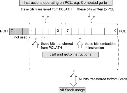
By Stack transfers
The Stack is a full 13 bits wide. Therefore any instruction, such as return, which uses the Stack causes a full 13-bit value to be transferred between Stack and Program Counter – there is no need to worry about looking after any missing bits.
By call and goto instructions
As the instruction word format in Figure 4.18 shows, these two instructions are formatted to provide only 11 bits of addressing. These 11 bits can address a range of 211, or 2K words, and thus represent the pages in Figure 7.4. When these instructions are used, the two ‘missing’ address bits are taken from bits 4 and 3 of the PCLATH register. It is up to the programmer to recognise if a branch over a page is to occur, and to set the bits appropriately. The data sheet [Ref. 7.1] contains an example of how to do this.
By writing to the PCL register
The PCL is written to directly in situations like the ‘computed go to’, as described in Section 5.4. Now only the lower eight bits of the Program Counter, in PCL, are adjusted directly and it is as if the programmer is working with 256-word pages. If an address boundary is to be crossed in a computed go to, then PCLATH must be set to the right value. For larger look-up tables this can be quite challenging; Ref. 5.1 gives examples of how to do it.
7.3.2 The 16F873A data memory and Special Function Registers
The 16F873A/874A data memory map, including all the SFRs, is shown in Figure 7.6. The sight of all those SFRs is initially unnerving. How is it possible to make sense of them all? Even more unnerving is the thought that most contain eight active bits, each of which has a function that probably needs to be understood. As always, we will find that a carefully staged approach will allow a good understanding to be developed. Most of these SFRs will be introduced and used, in the right context, over the next few chapters.
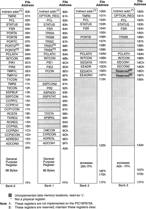
Structurally the memory is divided into four banks, which are selected by the values set in bits 6 and 5 of the Status register (Figure 7.3). The 7-bit ‘Direct Addr’ of Figure 7.2 is drawn from either of the first two instruction patterns of Figure 4.13. It gives the potential to address the 27, i.e. 128, memory locations which make up each bank. It is this 7-bit address, concatenated with the two bank select bits in the Status register, which form the 9-bit ‘RAM Addr’ seen in Figure 7.2, equivalent to the ‘File Address’ of Figure 7.6.
The first two data memory banks use this memory range to the full, the first one, for example, having 32 SFRs and 96 general-purpose memory locations. The higher two banks are of limited use in the 16F873A/874A. There is no general-purpose memory and most of the SFRs are just mirrored over from the other banks. Check carefully which SFRs are unique to Banks 3 and 4. What are they?
7.3.3 The Configuration Word
The Configuration Word of a 16 Series PIC microcontroller determines some of the programmable features of the microcontroller, which can be changed only when the device is programmed. The Configuration Word of the 16F87XA is shown in summary form in Figure 7.7. This reveals some of the underlying features of the microcontroller. The lower four bits, and the highest, are already familiar from the Configuration Word of the 16F84A (Figure 2.6). The two ‘new’ operating modes, of in-circuit programming and in-circuit debugging, are enabled through the Configuration Word. Similarly, the new and flexible code protect features and the detection of partial loss of power – a ‘brown-out’ – enabled by bit BOREN. These are described in the sections which follow.

7.4 ‘Special’ memory operations
A conventional microcontroller reads its instructions from non-volatile program memory and uses volatile RAM for storing temporary data. With the introduction of Flash memory, these distinctions between traditional memory usages are diminishing. This is because Flash memory technology is non-volatile and hence used for program memory. It can, however, also be very easily written to, so there is a temptation to use it for other forms of storage.
Because of its Flash memory technology, the 16F87XA allows – under certain restrictions – program memory to be written to while the program is running. It also allows the program memory to be programmed serially, if wanted, while the IC is in the target location. It also of course allows its EEPROM data memory to be accessed, through its special control registers. It is these memory functions that are covered in this section.
7.4.1 Accessing EEPROM and program memory
The ability to write to program memory, as just mentioned, is controlled by the settings of the WRT1 and WRT0 bits in the Configuration Word. It is worth looking back at these in Figure 7.7. It can be seen that they permit writing access to different blocks of program memory.
Interaction with program memory is through the same data and address registers that are used for EEPROM (EEDATA and EEADR), which were described in Section 2.4. These are only 8-bit registers, however, and program memory holds 14-bit words. Furthermore, it requires a 13-bit address to access the full 8K words (of the 16F876A and ’877A), or 12 bits to access 4K (of the 16F873A and ’874A). Therefore, a ‘high-byte’ register is added to each of EEDATA and EEADR. These extra registers are called EEDATH and EEADRH respectively, and are used for accessing program memory only.
The arrangement is depicted in Figure 7.8, with program memory at the top of the diagram and EEPROM at the bottom. The register pair formed by EEADRH and EEADR addresses program memory, while only EEADR addresses EEPROM. The situation is similar for data transfer, with EEDATH and EEDATA carrying data to and from program memory, and EEDATA alone being used for EEPROM data memory.
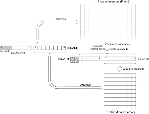
If a section of program memory is enabled, then blocks of four words must be written at the same time. This process is described in full in Ref. 7.1. Single word reads are, however, possible.
All data transfers are controlled by the EECON1 register, shown in Figure 7.9. It can be seen first of all that the MSB of this controls whether EEPROM or program memory is to be accessed. The other bits are similar to Figure 2.7 and therefore familiar. A major difference, however, is that the interrupt flag bit, EEIF, has been relocated, now being found in the PIR2 register (Figure 7.13).
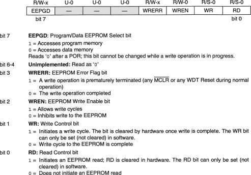
Accessing EEPROM and program memory is not entirely simple, and requires care in sequencing the actions correctly. Writing to each requires the codes 55H followed by AAH to be sent to the virtual EECON2 register. This adds further security to the process, aiming to ensure that accidental writes are not made. Code examples are given in Ref. 7.1. These can be adapted as appropriate.
If the CP bit of the Configuration Word is cleared, then it is impossible to read the program memory externally, for example using a programmer like the PICSTART Plus. This protects the intellectual property of the designer or maker of a product. This bit does not, however, affect internal access to program memory. Similar comments apply to the EEPROM memory, which is protected from external access by the CPD bit of the Configuration Word.
7.4.2 In-Circuit Serial Programming (ICSP)
All the 16F87XA microcontrollers can be programmed while in the target circuit. This is of great importance. In a development environment, it means that test programs can be downloaded straight to the microcontroller in the target system, without the need to remove it and put it in a programmer. In a production environment, it allows the microcontroller to be programmed in place, just before it leaves the factory. The very latest software can therefore be installed. Once the product is in use, it allows program updates to be made, possibly via the Internet and without the owner even knowing about it!
The disadvantage of in-circuit programming is that some pins have to be committed to the function, or at least must be carefully designed to be dual purpose, in such a way that the normal function of the pin does not impede the programming function. ICSP uses the pins shown in Table 7.1. The Derbot AGV uses ICSP – we will see it designed into the circuit.
TABLE 7.1 Pins used in In-Circuit Serial Programming
| Pin | Description |
|---|---|
| RB3 | Control input in Low-Voltage Programming mode (LVP configuration bit is 1) |
| RB6 | Clock input |
| RB7 | Data input/output |
| MCLR | Program mode select, programming voltage connection |
| Vdd | Power supply |
| Vss | Ground |
Under normal programming mode a high voltage, of around 13 V, is applied to the MCLR pin. A special case of ICSP dispenses with this high voltage, however. It is called the Low-Voltage Programming mode (LVP). This is enabled by the LVP bit in the Configuration Word, and allows the memory to be programmed using just the normal power supply VDD. Its disadvantage is that an extra pin, RB3, must be used, as Table 7.1 indicates. The pin is used just to control entry to and exit from this programming mode.
Aside from the hardware interconnection, ICSP requires very specific software routines to transfer the data serially into the microcontroller. These are not described further here, but full information can be found in Ref. 7.2.
7.5 The 16F873A interrupts
7.5.1 The interrupt structure
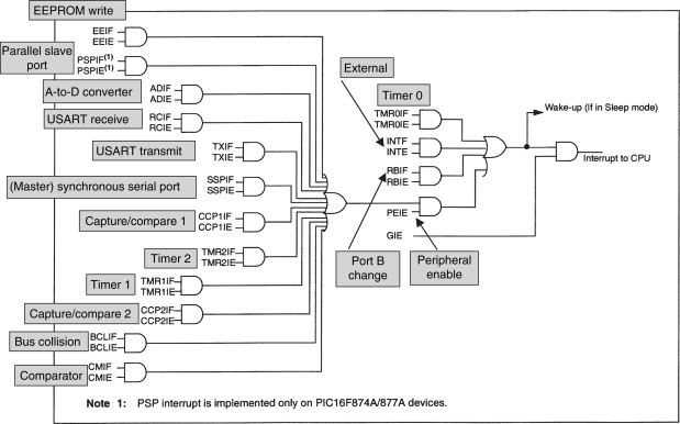
As a member of the 16 Series family of microcontrollers, the 16F873A is expected to fit into the structure of that family. This design strategy works well in places, but elsewhere tests the 16 Series structure to its limits. An example of this is the 16F873A interrupt structure, shown in Figure 7.10. Here we see the minimalist structure of the 16F84A (Figure 6.2) replicated to the right of the diagram. The EEPROM write complete interrupt is, however, replaced by a line linking across to the huge requirements of the larger microcontroller, with no less than 11 more interrupt sources connected. All of these are routed ultimately through to the single interrupt vector that we are familiar with, seen in the program memory map of Figure 7.4.
7.5.2 The interrupt registers
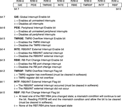
With 15 interrupt sources, the single INTCON register introduced in Figure 6.3 for the smaller 16 Series microcontroller can now only hold a small proportion of the overall number of flags and enable bits. The 16F87XA version is shown in Figure 7.11. Essentially it remains unchanged, except that the EEIE (EEPROM write complete enable) bit is replaced by the bit PEIE, seen in Figure 7.10. PEIE is the ‘Peripheral Interrupt Enable’ bit, acting as a subsidiary Global Enable, to all those interrupt sources upstream of the AND gate it drives. It must be set to 1 if any of the ‘upstream’ interrupts are to be used.
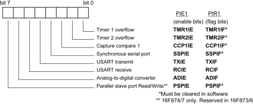
To augment the INTCON register, four new SFRs are added – PIE1 Peripheral Interrupt Enable and PIE2, which hold the enable bits and are located in memory bank 1, and PIR1 Peripheral Interrupt Request and PIR2, which hold the flag bits and are in memory bank 0. These are shown, in summary form, in Figures 7.12 and 7.13. It can be seen that PIE1 and PIR1 each follow the same pattern, as do PIE2 and PIR2. As would be expected, all active bits are reset to 0 on any form of power-up.

7.5.3 Interrupt identification and context saving
If more than one interrupt source is enabled, it will be necessary for the ISR to contain a program section at its beginning to identify which is the calling interrupt. This is similar to the case of the 16F84A, and the principle of Program Example 6.2 can be applied to meet this need.
When it comes to context saving, the 16F87XA again acts like the 16F84A, with only the return address being saved on the stack when an ISR is called. It is up to the programmer to save any other registers that are needed, usually the W and Status registers, at the start of the ISR, and retrieve them at the end. Program Example 6.4 can be adapted for this.
7.6 The 16F873A oscillator, reset and power supply
7.6.1 The clock oscillator
The 1687XA has exactly the same oscillator structure and range of options as the 16F84A, described in Section 3.5. The oscillator type is again selected by settings in the Configuration Word (Figure 7.7). It may be of interest at this point to look forward to Figure 7.19 and its accompanying description, to see actual oscilloscope traces of oscillator waveforms.
7.6.2 Reset and power supply
The reset structure is extremely similar to that of the 16F84A (Figure 2.10), with the exception that a new source has been added: the Brown-out Reset. A brown-out is a dip in the supply voltage. This form of power loss can be particularly dangerous, because it can pass unnoticed. Part of a circuit or system may keep going, whereas another part may temporarily fail or lose data. This reset is intended to ensure that the device is fully reset if a brown-out occurs. It is enabled by the BOREN bit of the Configuration Word. If BOREN is set high and a brown-out occurs, then the microcontroller is forced into reset. The device data [Ref. 7.1] quotes 4 V as being the typical voltage that triggers this form of reset. Apart from this the 16F87XA has almost identical power supply requirements to the 16F84A, as seen in Figure 3.16. A difference is that the minimum supply voltage is now clearly defined by the Brown-out Reset, if this is enabled.
With multiple sources of reset now available, it can be useful when programming to know which form of reset has most recently occurred. A Watchdog Timer reset is indicated by the ![]() bit of the Status register (Figure 7.3). Further information is provided by the
bit of the Status register (Figure 7.3). Further information is provided by the ![]() and
and ![]() bits of the PCON register (which has no other active bits). The first of these is set to 0 if a Power-on Reset occurs, the second if a brown-out occurs.
bits of the PCON register (which has no other active bits). The first of these is set to 0 if a Power-on Reset occurs, the second if a brown-out occurs.
7.7 The 16F873A parallel ports
It can be seen from Figure 7.2 that the PIC 16F873A has three ports, A, B and C. Ports A and B are similar to the ports of the 16F84A, except that more alternate functions are crowded onto the pins and Port A is now 6-bit, a 1-bit advance on the five bits of the 16F84A Port A. At reset all port bits are set to input. The port pin output characteristics, for a supply of 5 V, are shown in Figure 7.14. It can be deduced, following the same procedure as applied in Section 3.4.3, that the ‘typical’ output resistance at Logic 1 is approximately 70 Ω and around 22 Ω at Logic 0.
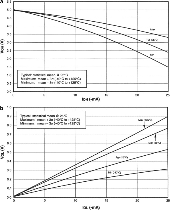
Figure 7.14 PIC 16F87XA port output characteristics. (a) Typical VOh vs. IOH (VDD = 5 V, –40 to 125°C). (b) Typical VOl vs. IOL (VDD = 5 V, –40 to 125°C)
The port characteristics are now surveyed in turn.
7.7.1 The 16F873A Port A
The six bits of Port A appear on pins 2–7 of the 16F873A, as can be seen in Figure 7.1. It is worth checking the accompanying key to work out the connections made to the pins. The port can be used for general-purpose bi-directional digital data. It is also shared with the Analog functions, notably the analog-to-digital converter (ADC) module and the comparators. While we meet both of these in Chapter 11, it is very important to note that on power-up the port bits are set as analog inputs. To use the port for digital purposes the ADCON1 register, described in Chapter 11, must be set appropriately. As with the 16F84A, the important Timer 0 input is on bit 4 of Port A.
Two of the Port A pin driver circuits are shown in Figure 7.15. It is useful to compare these with the equivalent 16F84A circuits, shown in Figure 3.11. With the added functionality of most pins, it is interesting to see how the peripherals that share the pins begin to ‘invade’ the pin driver circuit. A simple example is in Figure 7.15(a). This is almost the same as Figure 3.11(a), except the ADC peripheral, via the ‘Analog Input Mode’ line, can disable the digital input path of the port. A more extreme case is seen in Figure 7.15(b). Here a multiplexer is introduced in the digital output path. Now the peripheral, in this case the comparator circuit, can disable the normal port output and claim the output for its own purposes. In this case the microcontroller pin can be configured as the output of comparator 2 (C2OUT), rather than as the port bit output.

Figure 7.15 Block diagram of Port A pin driver circuits. (a) Pins RA0, 1, 2 and 3. (b) Pin RA5 (supplementary labels in shaded boxes added by the author)
The pin driver circuit for pin 4 is not shown. It is based on the circuit of Figure 3.11(b), but has added to it the multiplexer arrangement in the output path, as just described, for comparator 1. It keeps the Open Drain output of Figure 3.11(b).
An important point is emerging in this exploration of the pin driver circuits. The port pins are no longer simply controlled by the port ‘TRIS’ register. Other SFRs can have a major impact, disabling or reallocating a resource. This can lead to considerable programming frustration. A port may appear not to work because a peripheral SFR setting has reallocated its function. Let the programmer beware!
7.7.2 The 16F873A Port B
The interconnection of Port B can be seen in Figure 7.1 on pins 21–28 of the 16F873A. It remains a simple port, almost identical to that of the 16F84A. The pin driver circuits are effectively the same as those shown for the 16F84A in Figure 3.10. As seen in Figure 7.1 and Table 7.1, bits 3, 6 and 7 are used for ICSP. If ICSP is to be used, the designer must either not use these pins for any other purpose or use them in such a way that they are still available for the ICSP function.
7.7.3 The 16F873A Port C
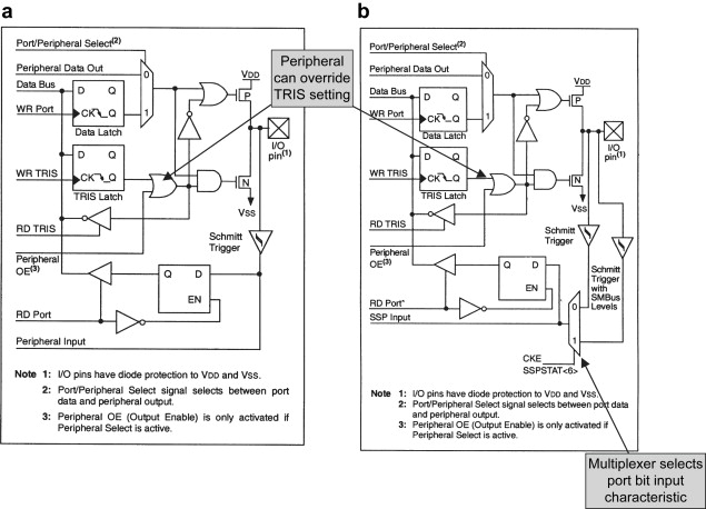
The Port C interconnection can be seen on pins 11–18 of the 16F873A (Figure 7.1). It is the most complex of the 16F873A ports. Its pins can simply be used as general-purpose digital input/output (I/O). Interestingly, all inputs now have Schmitt trigger characteristics. Aside from general-purpose digital I/O, Port C pins are shared with some of the more complex microcontroller peripherals, including those dealing with serial communication.
Diagrams of the Port C pin driver circuits are shown in Figure 7.16. At the heart of both of them it should still be possible to find the standard digital I/O port capability, such as we saw in the simple 16F84A pin drivers. To this is added the multiplexer on the output path, as seen just now for Port A. A further feature is that the peripheral can now take over the TRIS function, through the ‘Peripheral OE’ line, and the OR gate that it drives, as labelled in the diagram. A final modification of the standard port pin circuit is seen in Figure 7.16(b). Because the SMBus (system management bus) has defined input characteristics, there are now alternative input paths, one with standard Schmitt trigger inputs and the other with SMBus characteristics. This is not the end of the added complexity that serial I/O brings. Not appearing in Figure 7.15(b), but available on these pins if needed, is the full I/O interfacing capability of the inter-integrated circuit (I2C) serial standard. This can be glimpsed by looking forward to Figure 10.19.
7.8 Test, commission and diagnostic tools
As we are moving to a distinctly more complicated family of microcontrollers, it follows that we will be developing distinctly more complicated systems. It is therefore necessary to take time to consider here how we will test and commission such systems. The following sections explore equipment and techniques that can be used for such activities, and which will be applied as we develop the Derbot AGV design.
7.8.1 The challenge of testing an embedded system
Section 4.1.3 outlined the program development process, which included the use of a software simulator. When the program is downloaded to the hardware, however, our problems can increase. This is particularly the case if both hardware and program are untested. Then the developer can be left in the unhappy position experienced by all embedded systems developers at some time – of being confronted with a totally inanimate system, not having any idea of where the problem lies.
In the test procedure, the developer is confronted with broadly two types of problem:
• Design problems. These are problems in the design of hardware or software, leading to partial or total system non-function.
• Implementation problems. These are due to the way the design, which may be perfectly good, has been implemented. They include things like broken PCB tracks, failed or corrupted program download, or configuration bits not set in the download process. These problems can similarly lead to partial or total system non-function.
Each problem type can have the same sort of symptoms, yet it is important to be able to distinguish between the two, as the solution to each can be quite different.
Let us therefore try to establish a commissioning hierarchy, such that a systematic approach to testing and commissioning can be made. The layers of dependency that exist between different elements in an embedded system are shown in an informal way in Figure 7.17. Generally, in a test procedure one moves from the bottom to the top of this diagram. If a car does not have petrol it does not run. Similarly, if a microcontroller does not have the correct power supply, it does not run, however good the circuit or program may be. Nor will it run in any way if its oscillator is not running, if its Reset pin (![]() for a PIC) is active, or if the program has not downloaded properly. Once these four essential conditions are met, there is a chance of the program starting to run. If a system is entirely inactive, these must be the conditions that are tested first. Faults in this area are most likely to be in implementation, for example the crystal is not properly soldered to the board or program download has failed for some reason.
for a PIC) is active, or if the program has not downloaded properly. Once these four essential conditions are met, there is a chance of the program starting to run. If a system is entirely inactive, these must be the conditions that are tested first. Faults in this area are most likely to be in implementation, for example the crystal is not properly soldered to the board or program download has failed for some reason.
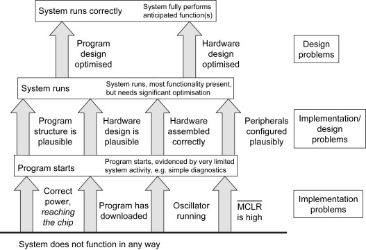
Once these fundamental conditions have been satisfied, a further set applies if the system is to run continuously and achieve a moderate level of functionality. As indicated, these include plausible circuit and program designs, correct hardware assembly and all the peripherals being configured appropriately to the situation. Here the word plausible is used to indicate that the design does not have fatal flaws, although it might have some features that need improvement. As the conditions indicated are met, the system should progress to a stage of optimisation. Now it shows a good level of functionality, although it is still imperfect in some areas. From here it is likely that further tests must be accompanied by ongoing incremental design development, which may lie in either the hardware or the program. Finally, one expects to see a system functioning to the full anticipated level of performance.
Given an understanding of the layers of dependence in an embedded system, how should the test procedure be implemented, particularly once the basic tests indicated by the bottom layer of Figure 7.17 have been completed? In Ref. 1.1, three ‘golden rules’ were identified for testing. These were:
• Divide and rule. Divide the system, both hardware and program, up into modules or subsystems which can be isolated as much as possible from each other, and test these separately. The system can then be put back together from ‘known good’ subsystems.
• Guilty until proven innocent. Make no assumptions that any part of the system is working correctly until you have demonstrated that it is. In other words, assume it doesn't work correctly until you have demonstrated that it does. This is the opposite of the court of law, where the accused is innocent until proven guilty.
• Work systematically, document ruthlessly. This can be expanded out to:
• Plan your test procedure ensuring that things are tested in a sensible and logical order. A starting point for the sequence is to some extent indicated in Figure 7.17. Start at the bottom of the diagram and work upwards.
• Work from good documents, updating them as necessary. As you work on your embedded system, have the up-to-date circuit diagram and program listing beside you. Always test by reference to these. Have appropriate data sheets (especially for the microcontroller in use) within easy reach. Update diagrams as needed, ensuring each new version has the revision date on it.
• Record your test results. This becomes increasingly important as the system becomes more complex. It is too easy, in a series of tests, to forget what the outcome of a single test was. However good your memory, in a week or two you will have forgotten anyway. With the result, record the circuit and program version in use.
To be successful in the test process, we need instruments that allow us to control and see what is going on. A number of these are now surveyed.
7.8.2 Oscilloscopes and logic analysers
An oscilloscope is the most powerful general-purpose instrument available in the electronics world. It allows simple and reasonably accurate measurements of voltage and time to be made, especially if they are DC or periodic. A standard oscilloscope is greatly enhanced by the addition of a storage facility. In this case it is possible to examine aperiodic signals, or single events, with reasonable ease. An oscilloscope is essential in the embedded world for examining the basic conditions of power supply, oscillator and simple port activity. With expertise, a good ’scope can be used for looking at more complex signals.
A logic analyser has some of the characteristics of an oscilloscope, in that it can also display the value of an input signal against time. The input signal, however, is assumed to be digital, so the display can only take one of two values, Logic 0 or Logic 1. The threshold applied is determined by the logic analyser, and is for many instruments adjustable. A usual characteristic of the logic analyser is that it has many inputs, for example 16, 32 or 48. Thus, it can be used to look at activity in data and/or address buses. Logic analysers usually carry a range of extra features, including memories that can store a history of the input values, and a complex triggering capability, which allows defined combinations of inputs to be identified and to cause a trigger. Logic analysers were most prominent in the days when systems were built of multiple ICs and there was a need to study bus activity. Now in many systems the ICs are very complex and the buses no longer accessible. They can still be very useful, however, in looking at complex digital activity, for example a parallel port or serial data flow.
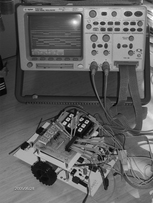
This book makes use of a wonderful instrument which combines features of both oscilloscope and logic analyser. This is the Agilent Mixed Signal Oscilloscope, with the 54622D model used here and pictured in Figure 7.18. It has two conventional oscilloscope inputs and 16 logic analyser inputs. Any combination of inputs can be displayed simultaneously. The ‘oscilloscope’ has fantastic triggering, signal analysis and storage facilities. Its combination of analog and digital capability reflects the mixture of analog and digital in most embedded systems. It thus forms a natural tool to undertake a comprehensive range of tests in the embedded environment.
Two screen images of oscillator signals, using the analog inputs of the Agilent ’scope, are shown in Figure 7.19. Note from information on the screen border that the vertical scales of both channels 1 and 2 are 2 V/cm and the horizontal scale is 1 μs/cm. The two small arrowheads appearing on the left of the screen indicate the 0 V reference position for each trace.
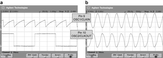
Figure 7.19 Oscillator traces from 16F873A devices. (a) RC oscillator, 800 kHz nominal. (b) Crystal oscillator, 4 MHz
The first screen is of an RC oscillator, applying the circuit of Figure 3.14(b). The upper trace shows the OSC1 microcontroller terminal, i.e. the junction of REXT and CEXT. The characteristic rising voltage of a capacitor charging through a resistor is seen, followed by its rapid discharge as the oscillator Schmitt trigger output switches to logic high. As Figure 3.14(b) indicates, the signal at the OSC2 pin is Fosc/4. This can be seen in the lower trace. Component values of REXT = 8.2 k and CEXT = 100 pF are chosen to give a nominal oscillator frequency of 700 kHz (i.e. a period of 1.43 μs). The actual signal can be seen to have a period of close to 1.4 μs (just over 700 kHz), with the Fosc/4 having a period of 5.6 μs. This is in reasonably good agreement with what is expected. It should be noted, however, that when the ’scope probe was removed from the OSC1 pin, the Fosc/4 period fell to 5.0 μs. Herein lies a pitfall of oscilloscope use – the probe plus oscilloscope input adds a loading capacitance (and resistance) to the circuit under test. Whether it has any impact of significance depends on the test circuit itself. In this case the loading is 15 pF approximately, which is placed directly in parallel with REXT, increasing its value by over 10 per cent! The measurement itself has introduced an error.
The second trace is of the microcontroller in HS crystal mode, and applies the circuit of Figure 3.14(a). Both microcontroller pins have similar, approximately sinusoidal, signals of the same frequency. One is the inverse of the other. It can be seen that the signal clearly has a period of 250 ns, confirming a frequency of 4 MHz.
7.8.3 In-circuit emulators
Oscilloscopes and logic analysers are very good for testing signals that are accessible and when the system is running. There are many situations, however, when we need to be able to undertake the same sort of tests we were doing with the software simulator in Chapter 5, for example testing specific sections of code or single-stepping, but now with the code running in the target hardware.
The solution to this need has been the ‘in-circuit emulator’ (ICE). This is a device which replaces the microcontroller in the circuit, replicating its action as closely as possible, but which remains linked back to a host computer. The host computer has the power to control program execution in much the same way as the software simulator does.
In-circuit emulators represent one of the most powerful ways of testing and commissioning an embedded system. They come with just a few disadvantages:
• They are very sophisticated pieces of equipment and hence expensive.
• They replicate one microcontroller or processor only, and hence a different one is needed for every different microcontroller used.
• There are areas where their action is imperfect, for example they are not usually good at replicating the action of the microcontroller in terms of the clock oscillator, and they may have power supply requirements which are less flexible than the microcontroller itself.
• They do not allow the genuine final operating condition of the system to be fully replicated – after all, the microcontroller itself has been removed.
7.8.4 On-chip debuggers
Given the benefits of the ICE, but also its disadvantages, it was natural for IC designers to ask themselves if they could actually design features of the ICE into the microcontroller itself. A good part of the ICE, after all, is a replica circuit of the microcontroller itself. Thus, a variety of on-chip test facilities came into being. Motorola (now Freescale) used the terminology ‘background debug mode’ (BDM), while Microchip uses the terminology ‘in-circuit debugger’ (ICD). We will explore this facility in detail, as it is now available on many PIC microcontrollers, including the 16F873A.
The advantages of the ICD approach can be summarised as:
• Testing is done with the target system substantially undisturbed.
• The ICD can also act as a programmer, downloading program code to the target microcontroller.
• The ICD approach is more flexible – connection, test and further download can be done ‘in the field’ as well as in the development lab.
The disadvantages of the ICD approach can be summarised as:
• Some microcontroller resources are taken by the ICD function; this includes a few I/O pins, some program memory and other internal resources.
• The target microcontroller must be functioning and with its clock running.
• It is generally less powerful than a fully fledged ICE system.
• Testing of certain aspects may still be imperfect. For example, when microcontroller operation has been halted by the ICD, peripherals may continue running, leading to erroneous results.
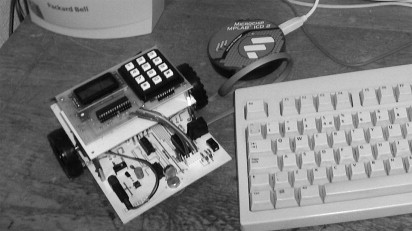
7.9 The Microchip in-circuit debugger (ICD 2)
The features of the Microchip ICD 2 system [Ref. 7.3] are illustrated in diagrammatic form in Figure 7.20; the host computer is linked to the target system via a special adaptor unit or pod. This is seen in a real system in Figure 7.21, where an ICD 2 pod is shown linked to a Derbot AGV. The ICD is controlled from the host computer, which must be running MPLAB. The ICD 2 pod links to the host computer via a USB cable. An RS232 link may also be used. It then connects to the target system via another cable, having five interconnections. These are shown in the diagram and are the same as those for ICSP, except that the low-voltage programming pin, bit 3 of Port B, is not used. The internal microcontroller resources needed by the ICD are also shown in the diagram, and include elements of program memory, data memory and the Stack.
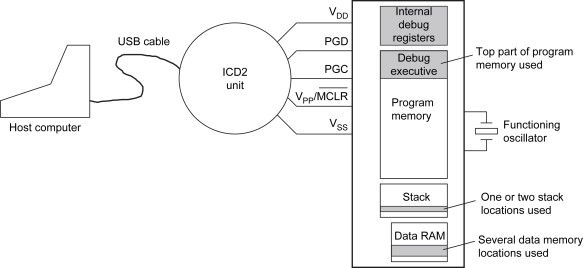
The ICD 2 can be used as a debugger, in which case it can program the microcontroller, at the same time downloading its own ‘debug executive’, which is loaded into the high end of the program memory. Running from MPLAB it can then execute all the functions of the MPLAB simulator, as introduced in Chapters 4 and 5, except that now the program is actually running in the hardware. The ICD 2 can also be used simply as a programmer, in which case it replicates the action of programmers like the PICSTART Plus, described in Chapter 4. The operating mode is selected from within MPLAB.
The normal use of the ICD 2 in the development cycle is to download the program under test to the microcontroller with the ICD in debug mode. The program is then debugged using all the facilities of the ICD. When a fully functioning version has been developed, the ICD is switched to programmer mode. The program is then downloaded again, this time without the special features of the debugger, and the microcontroller can run in its normal operating mode.
Use of the ICD 2 will be described in a simple Derbot-based tutorial following description of the first Derbot build.
7.10 Applying the 16F873A: the Derbot AGV
Following the descriptions earlier in this chapter, we turn now to seeing the 16F873A applied in a practical situation, the Derbot AGV. The Derbot block diagram is shown in Figure 1.5 and its circuit diagram in Figure A3.1. Some of the underlying considerations in the design and application of the Derbot are described in Appendix 4.
7.10.1 Power supply, oscillator and reset
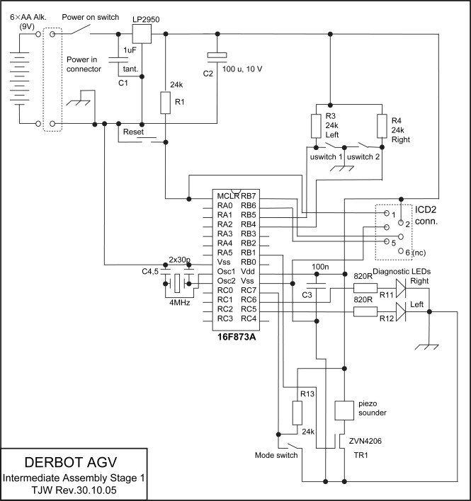
The power needs of the Derbot are twofold: to power the motors and to power the microcontroller circuit and all associated sensors and displays. While low-voltage motors, running from 2 or 3 V, are available, it is less easy to arrange the necessary switching circuits to run at this voltage. Experimentation with several motors, however, showed that adequate torque and speed could be obtained from a motor running from around 9 V, with a tolerable supply current. This voltage fitted well with currently available motor interface ICs, like the L293D, which is used. The second power supply need is for the microcontroller circuit. While this could have been supplied unregulated, as in the ping-pong project, there are a number of sensors, particularly the light-dependent resistors and reflective opto-sensors, which require stable operating conditions for correct results. Therefore, a regulated supply was chosen.
The Derbot is therefore normally supplied from six ‘AA’ Alkaline cells, giving an overall nominal supply of 9 V. This voltage is used ‘raw’ for the motor supply. For supply to the microcontroller and associated circuit it is regulated down to 5 V, using a National Semiconductors LP2950 low-power voltage regulator. A number of the system elements, for example the opto-sensors, rely on this regulated voltage to operate correctly.
As there are precise timing requirements in the application, a crystal oscillator was selected; 4 MHz was chosen as the oscillator frequency, to allow simple timing functions to be derived from the resulting 1 μs instruction cycle time.
7.10.2 Use of the parallel ports
As can be seen, Derbot has extensive I/O requirements, although not all of these may be implemented in any one version of it. They are listed in Table 7.2. Some simply require general-purpose parallel I/O. Others, as indicated, are special-purpose functions that link to specific peripherals or I/O through uniquely identified pins. These functions were therefore allocated immediately to their special-purpose pins. Like the port pins themselves, there are some shared functions apparent in the table. These are mainly used in the short term for demonstration purposes.
| Function | Data direction | Microcontroller peripheral used | Port and pin allocation |
|---|---|---|---|
| In-circuit debug | Bi-directional | Parallel port | Port B, 6 and 7 |
| ‘Bump’ microswitches | Input | Parallel port | Port B, 4 and 5 |
| Servo drive | Output | Parallel port | Port B, 3 |
| Opto-sensor enable | Output | Parallel port | Port B, 2 |
| Piezo sounder | Output | Parallel port | Port B, 1 |
| Interrupt | Input | Parallel port/interrupt | Port B, 0 |
| Mode switch, also USART RX | Input | Parallel port | Port C, 7 |
| Diagnostic LED, also ultrasound echo, also USART TX | Parallel port | Port C, 6 | |
| Diagnostic LED, also ultrasound pulse | Output | Parallel port | Port C, 5 |
| I2C, serial data | Bi-directional | Synchronous serial port | Port C, 4 |
| I2C, serial clock | Bi-directional | Synchronous serial port | Port C, 3 |
| Right motor PWM drive, also PWM demo, TPs 1 and 2 | Output | PWM | Port C, 2 |
| Left motor PWM drive | Output | PWM | Port C, 1 |
| Reflective opto-sensor | Input | Timer 1 | Port C, 0 |
| Left motor enable | Output | Parallel port | Port A, 5 |
| Reflective opto-sensor | Input | Timer 0 | Port A, 4 |
| Light sensor, rear | Input | Analog-to-digital converter (ADC) | Port A, 3 |
| Right motor enable | Output | Parallel port | Port A, 2 |
| Light sensor, left | Input | ADC | Port A, 1 |
| Light sensor, right | Input | ADC | Port A, 0 |
The Derbot general-purpose I/O can be allocated with some degree of flexibility. The choice is only influenced by the opportunity of Schmitt trigger input, internal pull-up resistor (Port B) and of course the physical position on the microcontroller IC. The implementation of Derbot switch and LED interfacing is considered here; other interfacing is considered in later chapters.
Switch interfacing
The Derbot AGV uses the mode switch, a user control which can cause the robot to switch between two modes, and a couple of microswitches, which are used for bump sensing. Electrically these switches are the same, being SPST, and so can be connected using the diagram of Figure 3.7(b). A regular pull-up resistor or the Port B pull-up can be used. In the latter case, it is worth noting that pull-ups will be switched on for all Port B bits used as inputs, regardless of whether they are wanted or not. As only three pull-ups are required, it was decided to use external components and not activate those of Port B.
LED driving
Two general-purpose diagnostic LEDs are included in the circuit. These can be used for any purpose that the programmer wishes. The high-efficiency red type chosen gives excellent output at very low currents. Tests showed that adequate visibility could be obtained with a current in the region of 3.5 mA. Using the characteristics of Figure 3.8(a), the forward voltages across the LED for this current will be around 1.88 V, and from Figure 7.14(a) the port bit output voltage will be around 4.7 V. Hence, applying equation (3.1):
820 Ω is a close ‘preferred value’ and was found to provide good visibility.
7.10.3 Assembling the hardware
If you are building up a Derbot AGV, then use the component layout diagram on the book’s companion website and assemble the following:
Having done this, you will have a PCB assembled with the circuit shown in Figure 7.22.
7.11 Downloading, testing and running a simple program with ICD 2
Let us now attempt running a program for the new hardware design and, if you have access to one, the ICD 2.
7.11.1 A first Derbot program
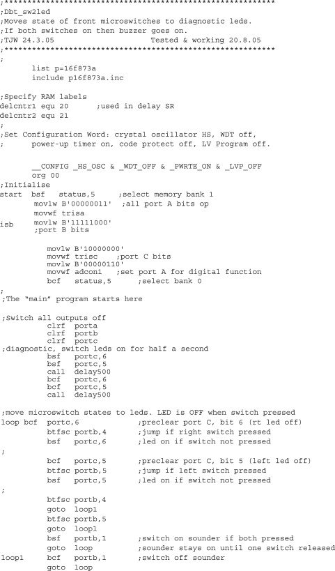
Program Example 7.1 is a very simple test program for the embryonic Derbot AGV, as just constructed. It simply tests the states of the front microswitches and sets or clears the diagnostic LEDs accordingly. If both switches are pressed, the sounder comes on.
In MPLAB create a project Dbt_sw2led (or name of your choice) and copy the program Dbt_sw2led.asm from the book’s companion website, or enter it by hand; it is shown in its entirety in the printed example. Build the project in the usual way. If you do not have an ICD 2, then download the program to the PIC, using your usual programmer, for example the PICSTART Plus, as described in Chapter 4.
7.11.2 Applying the ICD 2
The following assumes you have an ICD 2 or later a version of it. It is a very brief introduction, written in the expectation that you already have knowledge of the MPLAB simulator, whose features are used by the ICD 2. Further expertise can then be gained by experimentation and reading the full manual [Ref. 7.3].
Ensure, by reading the ‘Getting Started’ section of the manual, that the ICD 2 is configured correctly for your computer and operating system. Connect it between computer and AGV, as illustrated in Figure 7.20. Open MPLAB and open the project that you have created, containing Program Example 7.1. Set the ICD to operate initially in debug mode, by clicking Debugger > Select Tool > MPLAB ICD 2. Then complete the connection to the AGV by
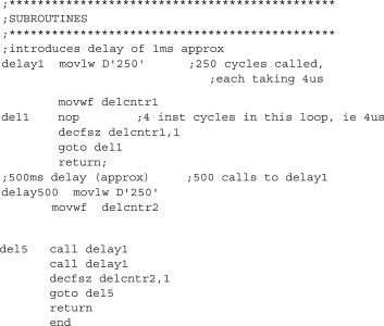
pressing Debugger > Connect. The ICD will run a self-test, which checks for the presence of power supply, as well as its ability to apply the correct voltages to the lines it controls. If the target system is powered and working, the ICD 2 should pass the self-test and will be able to identify the microcontroller. It will display a message indicating whether it has passed the test and issue an MPLAB ICD 2 Ready message. The drop-down menu under Debugger will then become active, as will the toolbar, as seen in Figure 7.23. An extra toolbar, unique to the ICD 2, will also appear. This appears to the right of the figure, and allows the user to read program memory, download to it and reset the ICD. Notice, however, that if on the main toolbar Programmer > Select Programmer is pressed, the menu will indicate that no programmer is selected. This is because in this mode the ability to program is only available within the ICD debugger facility.
Ensuring that the Derbot is switched on, download the program memory, using either the toolbar button of Figure 7.23 or Debugger > Program. Open a Watch window, as described in Chapter 4, and display registers PCL, PORTB and PORTC. Then start single-stepping through the program, using the Step Over function to skip the delay routines. Once in the main loop, try pressing the microswitches in turn, and see the response of the Port values in the Watch window as you step. Unlike when using the simulator, it is actual values from the hardware that are being transmitted back to the display you are seeing. Try setting or clearing port bits from your computer, and see how you can switch the Derbot LEDs themselves on and off in this way. As with the simulator, breakpoints can be set in the program by double-clicking on any line.
To finally program a product, the ICD 2 should be switched to programmer mode. On the top toolbar click Programmer > Select Programmer > MPLAB ICD 2 and then Programmer > Connect (an automatic connection mode is also possible). A check back at the Debugger menu will show that there is now no debugger selected. It is now possible to program and read the memory. The pull-down menu and programmer toolbar are available, as shown in Figure 7.24. Notice that Reset can be controlled from the screen. When programming is complete, Reset is left active. It can be released using the toolbar button shown, and the program then runs immediately.

7.11.3 Setting the configuration bits within the program
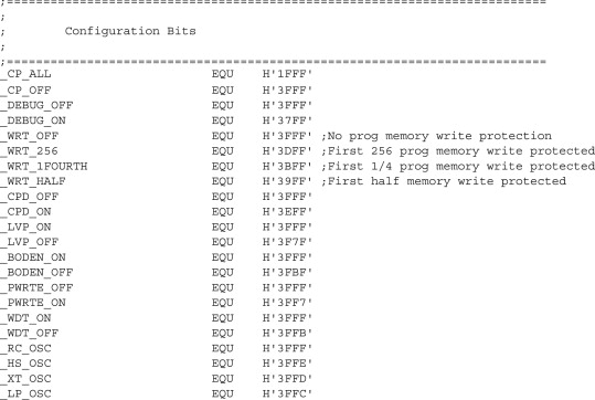
The 16F873A has more configuration bits than the 16F84A and it is easy to make an error when setting them in the MPLAB window. Incorrect settings can lead to very odd behaviour in the target embedded system or to no behaviour at all! It is, however, possible to set the configuration bits in the program by using the __CONFIG assembler directive. This directive uses symbols that are defined in the microcontroller Include File. The relevant section for the 16F873A is shown as Program Example 7.2. It can be seen that each hexadecimal value that a symbol equates to is derived from the Configuration Word setting shown in summary in Figure 7.7. As combinations of these are ANDed together, a final setting for the Configuration Word is formed. The setting used, seen in the program excerpt shown here, can be applied to all Derbot programs based on the 16F873A.
;Set Configuration Word: crystal oscillator HS, WDT off,
; power-up timer on, code protect off, LV Program off.
__CONFIG _HS_OSC & _WDT_OFF & _PWRTE_ON & _LVP_OFF
Even with this setting in the program, there is a danger that a change could be made inadvertently in the MPLAB Configuration Bits window. You can demonstrate this by building Program Example 7.1. Look at the configuration bit settings in the window – they are correct. However, it is possible at this stage to introduce an error by making a change in the window. Whatever is now shown in the window will be downloaded to the program memory on the next program download. This danger can be removed by clicking Configure > Settings > Program Loading and checking the ‘Clear configuration bits upon loading the program’ box. Now, on program download, the window setting is cleared and the configuration bits defined in the program are downloaded.
7.12 Taking things further – the 16F874A/16F877A Ports D and E
Looking at Figure 7.1(b), one can see that the 16F874A and 16F877A have two extra ports, the 8-bit Port D and the 3-bit Port E. Either port can be used for general-purpose I/O, like any of the other ports. The block diagram of Port D, when configured for normal digital I/O, is shown in Figure 7.25(a). An alternative function for Port E is to provide three further analog inputs. Because of this, Port E is also under the control of one of the registers that control the ADC, ADCON1. The setting of this determines whether the port is used for digital or analog signals.

Figure 7.25 Block diagrams of Port D pin driver circuits. (a) In I/O mode. (b) As parallel slave port (supplementary labels in shaded boxes added by the author)
Together, Ports D and E can also form the parallel slave port. The ports are put into this mode by setting the PSPMODE bit in the TRISE register (Figure 7.26). The purpose of this mode is to allow the microcontroller to interface as a slave to a data bus, controlled perhaps by a microprocessor. The Port E bits must be set as inputs (with digital mode selected in ADCON1); the state of TRISD is, however, immaterial. Ports D and E are then configured as in Figure 7.25(b). The diagram shows 1 bit of Port D, together with the three control lines, ![]() ,
, ![]() and
and ![]() . These are the three bits of Port E, now configured for this purpose. Notice that there is an output latch and an input latch for each Port D bit.
. These are the three bits of Port E, now configured for this purpose. Notice that there is an output latch and an input latch for each Port D bit.
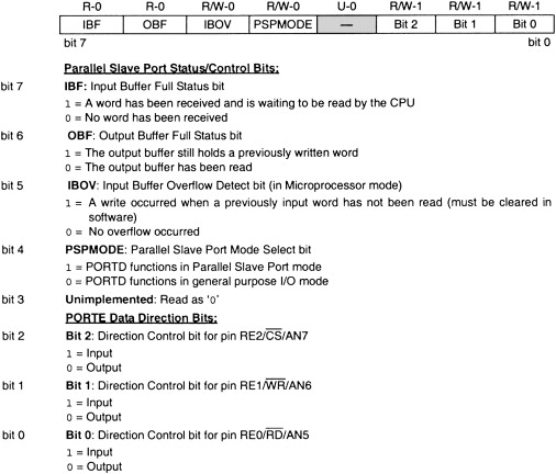
An example application for the parallel slave port appears in Figure 7.27. Here the port is connected to a data bus and control lines that form part of a larger system, controlled by a microprocessor. The 16F874A program can write data to the port, in which case bit OBF of TRISE is set. If ![]() and
and ![]() are taken low by the external circuit, then the port outputs the data held on its output latches onto the external bus. This action clears OBF. If
are taken low by the external circuit, then the port outputs the data held on its output latches onto the external bus. This action clears OBF. If ![]() and
and ![]() are taken low, the port latches data from the bus into its input latches, and bit IBF of TRISE is set. IBF is cleared when the port is read by the microcontroller program. If, however, the external circuit writes to the port again, before the previous word has been read, then the IBOV bit of TRISE is set. The interrupt flag PSPIF (Figure 7.10) is set when either a slave write or read is completed by the external circuit. This flag must be cleared in the software.
are taken low, the port latches data from the bus into its input latches, and bit IBF of TRISE is set. IBF is cleared when the port is read by the microcontroller program. If, however, the external circuit writes to the port again, before the previous word has been read, then the IBOV bit of TRISE is set. The interrupt flag PSPIF (Figure 7.10) is set when either a slave write or read is completed by the external circuit. This flag must be cleared in the software.

Summary
• The 16F87XA group of microcontrollers is an important subset of the 16 Series family. Its added capability is achieved by the inclusion of a powerful set of peripherals, along with memory upgrades.
• The central architecture of the 16F87XA group is the same as other microcontrollers in the PIC 16 Series of microcontrollers, with the same instruction set.
• Testing of an embedded system must be undertaken systematically, applying the best tools that are available to do the job.
• In-circuit debugging is a powerful technique for testing and commissioning both program and hardware, allowing minimum invasiveness.
7.1. PIC 16F87XA Data Sheet (2003). Microchip Technology Inc., Reference no. DS39582B; www.microchip.com
7.2. PIC 16F87XA Flash Memory Programming Specification (2002). Microchip Technology Inc., Reference no. DS39589. www.microchip.com
7.3. MPLAB ICD 2 In-Circuit Debugger User's Guide (2005). Microchip Technology Inc., Reference no. DS51331B. www.microchip.com
Question and exercises
1. What are the values in the W register, and of the Z, DC and C bits of the 16F873A Status register, after each of the following pairs of operations:
2. At a certain moment in a 16F873A program execution, the readings shown in the table below were noted. Deduce the interrupt settings that have been made, and suggest at what possible moment in program execution this sample has been taken.
SFR Value SFR Value INTCON 01010010 PIE1 00001000 PIE2 01000000 PIR1 00000000 PIR2 00000000 3. An application using the 16F873A requires three interrupts to be enabled: Timer 0 overflow, External Interrupt, and A-to-D converter. Which registers should be set for this, and how?
4. Four Port B bits of a 16F873A are used as outputs; two will drive green LEDs and two will drive red. Kingbright LEDs are to be used, with characteristics as shown in Figure 3.8. The red LEDs are to be lit with a current of 5 mA when the associated port bit is at Logic 1. The green are to be lit with a current of 12 mA when the bit is at Logic 0. The power supply is 5 V. Calculate the values of the series resistors needed. Note: this is a repeat of Question 3.7, applying a different microcontroller and different supply voltage.
5. Program Example 7.1 is written for the circuit of Figure 9.22. Rewrite the initialization section of that Program Example, starting from the label loop, so that it is appropriate for the circuit diagram of Figure 9.20.
6. You have just constructed a Derbot to build stage 1 (Figure 7.22) using a microcontroller known to be loaded with Program Example 7.1. Identify possible causes of each of the following faults, each occurring just after power-up. Explain how the fault could be confirmed and possibly corrected.
• Power appears to be reaching the voltage regulator, but its output is 0 V. The regulator is possibly warm to the touch.
• Smoke is seen to come from the electrolytic or tantalum capacitors.
• The program appears to start executing. Suddenly, it starts again, doing this periodically.
• As directly above, but program restart appears to happen randomly, possibly associated with you touching the board.
• One or both LEDs come on, apparently at random, possibly associated with you touching the board. The microswitch, however, does not influence the LED condition.