
CHAPTER 13 Smarter systems and the PIC 18F2420
In this book so far we have studied microcontrollers from the PIC 16 Series, large and small. While these are good microcontrollers, certain tensions and limitations have emerged. Some aspects of the hardware are limiting, for example the small size of the stack or the way all those interrupt sources have to share a single interrupt vector. As far as the instruction set is concerned, we recognise the value of the RISC approach. The absence of certain styles of instruction is, however, frustrating. Branch instructions, for example, have to be made out of a combination of skip and goto. Furthermore, the prospect of crafting major programs out of all those little Assembler instructions is becoming increasingly daunting.
Many of these limitations are experienced because the 16 Series has retained a core which was designed with only modest applications in mind. Now the number of peripherals has increased dramatically and memory sizes have soared. It is worth having a new beginning, addressing the issues that limit the 16 Series and rethinking the design of the microcontroller core. This is the basis of the PIC 18 Series.
When advancing from the 16F84A, we found that the 16F873A and then the 16F883 kept the core and enhanced the peripherals. We will now find that the 18 Series devices advance the core, while keeping peripherals reasonably constant. A very new style of microcontroller is produced as a result. The distinctive advantages of the PIC structure – RISC architecture, high speed and so on – are of course retained. New features appear, however, that allow the PIC microcontroller to move into a bigger arena – features which enhance real-time operation, ease the use of high-level languages and allow interaction with much larger memories. Other important developments, like the move to nanoWatt technology, appear in both 16 and 18 Series.
This chapter anticipates that the reader is upgrading from a 16 Series device, although it doesn't matter significantly if he/she is not. It draws on knowledge of the 16 Series and makes comparisons, as it is interesting to see how design concepts have evolved. The description of the instruction set in particular is developed through such a comparison.
From this chapter onwards the book will use mainly the C language for programming, rather than Assembler. It is therefore less important to know the microcontroller hardware in intimate detail. The C compiler looks after that side of things. This comes as quite a relief, as the 18 Series devices are not simple. For this reason, you will find that some topics in this chapter are introduced with a ‘lighter touch’ than equivalent sections in, say, Chapter 7. This is particularly the case with the peripherals. We will find C library functions to undertake all interaction with the peripherals, and in normal usage we just won't need an intimate knowledge of them. Energies previously spent (while programming in Assembler) in learning every fine detail of a peripheral can therefore be diverted to the creative task of writing working programs. This is a liberating step.
Of the 18 Series the 18F2420, along with its close relations in the 18FXX20 sub-family (i.e. 18F2520, 18F4420, 18F4520), are chosen for detailed study. We use the 18F2420 as it is a comparatively simple example of the 18 Series.
This chapter aims to introduce:
• The architecture of the 18 Series microcontroller, focusing on the 18F2420.
• The memory structure, and how it is accessed and addressed.
• The 18FXX20 peripherals, in most cases drawing on knowledge of their 16 Series equivalents.
13.1 The main idea – the PIC 18 Series and the 18F2420
The PIC 18 Series microcontrollers dramatically enhance the PIC core, making it suitable for more advanced embedded projects. Despite many features which are new, it has been designed to make upwards migration from a 16 Series device easy, so that the designer making this move will find many things which are familiar. The principal characteristics we shall see are as follows.
Similar to the 16 Series
New for the 18 Series
• The number of instructions has more than doubled, with a 16-bit instruction word.
• Radically different approach to memory structures, with increased memory size.
The 18FXX20 microcontrollers form a set of four closely related devices, whose main characteristics are represented in Table 13.1. In many ways this table is similar to the 16F87XA microcontrollers in Table 2.1. All 18FXX20 devices have an instruction set of 75 instructions, with a clock oscillator that can run from DC to 40 MHz. There are also ‘low-power’ versions of each microcontroller available, coded 18LFXX20. The full manufacturer's data on this family is found in Ref. 13.1.
TABLE 13.1 The 18FXX20 sub-family
| Device number | No. of pins∗ | Memory | Peripherals/special features |
|---|---|---|---|
| 18F2420 | 28 |
|
|
| 18F2520 | 28 |
|
|
| 18F4420 | 40 |
|
|
| 18F4520 | 40 |
|
ADC, analog-to-digital converter; PWM, pulse width modulation.
∗ For DIP package only.
∗∗ Single-word instructions, noting that some are two words.
The pin connections of the 18FXX20 family, for the dual-in-line packages, are shown in Figure 13.1. The figure is very similar to Figure 7.1, with the ports, power supply, oscillator and reset lying in the same places. This of course allows upgrade with minimum change.

13.2 The 18F2420/2520 block diagram and Status register
The block diagram of the 18F2X20 microcontrollers, which are the 28-pin devices of Figure 13.1(a), is shown in Figure 13.2. Take some time to identify the principal features of this important diagram.
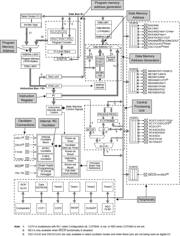
Figure 13.2 The PIC 18F2420/2520 block diagram (supplementary labels in shaded boxes added by the author)
Almost central to the diagram is the CPU (Central Processing Unit), containing the 8-bit ALU (Arithmetic Logic Unit), the Working register ‘W’ (sometimes called the accumulator) and an 8-bit × 8-bit hardware multiply unit. CPU action is determined by the instruction received from the program memory, which is transferred through the Instruction register. This is seen above and to the left of the CPU block. An important element of the CPU, though not shown in this diagram, is the Status register.
Program memory is seen to the top left of the diagram. Its address bus enters the memory ‘Address Latch’. With its 21 bits, it is possible to address 221 locations, i.e. 2 097 152 (2 Mbyte) locations. Table 13.1 shows that the 18F2420 only needs to address 16K locations, which require only 14 bits. The other lines are therefore redundant here. The 16-bit bus carrying the instruction word is seen leaving the ‘program memory data latch’. This can be seen working its way down to, among other places, the Instruction register, already mentioned. To the right of the program memory is an area labelled ‘program memory address generation’. Central to this of course is the Program Counter. Below the Program Counter is the Stack, which contains 31 locations. A table pointer provides a means of accessing tables or other data in program memory, under user program control.
The data memory is seen almost top centre of the diagram. Like the program memory, its address generation forms a significant block of the diagram overall, with a bank of File Select Registers (FSR0, for example) and a Bank Select Register (BSR). The data memory address is 12 bits, which can address 4096 bytes. Again, Table 13.1 shows us that this address bus is not fully exploited. Data transfer to and from the data memory is through the main data bus.
With the separate address bus and data input/output for each of program memory and data memory, we can at this point confirm the underlying Harvard structure of the microcontroller.
Power supply connections for the microcontroller, VDD and VSS, appear towards the bottom left of the diagram. A Look back at Figure 13.1 shows that two pins are dedicated to the VSS connection for either of the two packages shown. This ensures a good 0 V connection. The smaller package has a single VDD connection, while the larger has two. Associated with power supply is the Power-on Reset, which ensures reset when power is switched on; the Power-up Timer, which can be used to maintain the microcontroller in a state of reset for a fixed time after power-up; and the Brown-out Reset, which will force the microcontroller into reset if the power supply dips.
Oscillator inputs, both for the main oscillator and for Timer 1, are seen at the left of the diagram. To the right of these is the internal oscillator block, containing the 8 MHz oscillator and internal RC oscillator. Again, to the right of this is a block of functions which deal with start-up and system reliability, like the Power-up and Watchdog Timers.
Finally, the parallel ports, containing both their input/output function and all interconnection with the peripherals, are placed on the right-hand side. The other peripherals appear along the bottom of the diagram. Among these is another memory block, using EEPROM technology.
As an important part of the CPU, the Status register is shown in Figure 13.3. It contains a full five bits of status information on the operation most recently performed by the microcontroller. The limited number of Status bits (Figure 7.3) is arguably one of the weaknesses of the 16 Series microcontroller. The 18 Series adds two new bits. These are OV (bit 3), which signals an overflow of the 7-bit two's complement range, and N, which indicates that a two's complement number is negative. As the sign bit in a two's complement number is the MSB, the N bit is simply the MSB of the result. These extra bits allow improved program branching and better mathematical capability. The other information in the figure is self-explanatory.

13.3 The 18 Series instruction set
The instruction set of the PIC 18 Series is shown in Appendix 5, with 75 distinct instructions! It is a super-set of the PIC 16 and 17 Series instruction sets, so any program which runs on one of those microcontrollers can be expected to run on the 18 Series. With this many instructions, the set begins to have a CISC (Complex Instruction Set Computer – see Chapter 1) feel to it, losing some of the simplicity we expect of RISC. There is also an ‘extended’ 18 Series instruction set, which adds a number of instructions. These are described below.
Looking at Table A5.1, it seems a daunting prospect to get to know all those instructions. The good news is: we don't need to! After this chapter, almost all the programming we do will be in C, so someone else can worry about Assembler. However, an overview is still useful – we do, after all, need Assembler inserts in C sometimes.
For those migrating to the 18 Series from the 16 Series, Table 13.2 will be interesting. This gives a brief comparison of the two instruction sets. The first column lists all 16 Series instructions, approximately in the order given in Appendix 1. The second column gives the 18 Series equivalent, where there is one, and also lists all instructions that are completely ‘new’.
TABLE 13.2 Comparison of 16 Series and 18 Series instruction sets
| 16 Series instruction | 18 Series equivalents | Description |
|---|---|---|
| Byte-oriented file register operations | ||
| addwf f,d | ||
| andwf f,d | andwf f,d,a | And W and f |
| clrf f | clrf f,a | Clear f |
| clrw | – | Clear W |
| comf f,d | comf f,d,a | Complement f |
| decf f,d | decf f,d,a | Decrement f |
| incf f,d | incf f,d,a | Increment f |
| incfsz f,d | ||
| iorwf f,d | iorwf f,d,a | Inclusive OR f with W |
| movwf f | movwf f,a | Move W to f |
| nop | ||
| – | mulwf f,a | Multipy W and f |
| – | negf f,a | Negate f |
| rlf f,d | ||
| rrf f,d | ||
| – | set f | Set f |
| subwf f,d | ||
| – | subfwb f,d,a | Subtract f from W with borrow |
| swapf f,d | swapf f,d,a | Swap nibbles in f |
| – | tstfsz f,a | Test f, skip if zero |
| xorwf f,d | xorwf f,d,a | Exclusive OR W with f |
| Bit-oriented file register operations | ||
| bcf f,b | bcf f,b,a | Clear bit b in register f |
| bsf f,b | bsf f,b,a | Set bit b in register f |
| – | btg f,d,a | Toggle bit b in register f |
| btfsc f,b | btfsc f,b,a | Test bit b in f, skip if clear |
| btfss f,b | btfss f,b,a | Test bit b in f, skip if set |
| Literal operations | ||
| addlw k | addlw k | Add literal to W |
| andlw k | andlw k | And literal with W |
| iorlw k | iorlw k | Inclusive OR literal with W |
| movlw k | movlw k | Move literal to W |
| – | movlb | Move literal to BSR |
| – | lfsr f,k | Load FSR f with 12-bit literal k |
| – | mullw | Multiply literal with W |
| sublw k | sublw k | Subtract W from literal |
| xorlw k | xorlw k | Exclusive OR literal with W |
| Control operations | ||
| call k | Call subroutine, with (s = 1) or without (s = 0) saving context to Stack Relative call to subroutine | |
| clrwdt | clrwdt | Clear Watchdog Timer |
| – | daw | Decimal adjust W |
| goto k | goto n | Go to absolute address, where k/n address anywhere in program memory space |
| – | pop | Pop top of return stack (TOS) |
| – | push | Push top of return stack (TOS) |
| – | reset | Software reset |
| retfie | retfie s | Return from interrupt, with (s = 1) or without (s = 0) retrieving context from Stack |
| retlw k | retlw k | Return with literal in W |
| return | return s | Return from subroutine, with (s = 1) or without (s = 0) retrieving context from Stack |
| sleep | sleep | Go into standby mode |
| – | bc, bn, bnc, bnn, bnov, bnz, bov, bz | Eight conditional branch instructions, one for each state of Status register bits N, OV, Z, C, all with 8-bit twos complement relative address n |
| – | bra n | Branch unconditionally 8-bit twos complement relative address n |
| Program memory Table Read/Write operations | ||
| – | tblrd∗, tblrd∗+, tblrd∗–, tblrd+∗ | Four Table Read instructions, with pointer change respectively no change, post-increment, post-decrement, pre-increment |
| – | tblwt∗, tblwt∗+, tblwt∗-, tblwt+∗ | Four Table Write instructions, with pointer change respectively: no change, post-increment, post-decrement, pre-increment |
To explore the 18 Series instructions, let's start by looking at the first two columns of Table A5.1. These give the Assembler mnemonic of the instruction with its operands, followed by what the instruction does. The symbols used for the operands, for example a, d or f, are explained in Table A5.2. While some of these are familiar from the 16 Series, the operand bit a is new and leads to the possibility of instructions with three operands. This defines the memory area called ‘Access RAM’ described later in this chapter. Through this bit, the programmer now has a choice of whether to use Access RAM or not.
The third column of Table A5.1 indicates how many instruction cycles the instruction takes to execute. As we expect with a RISC and pipelined structure, all normal instructions execute in a single cycle. Those which cause a program branch take two. Skip instructions take one cycle if there is no skip, two if followed by a single-word instruction and three if followed by a two-word instruction. A small number of complex instructions also take more than one cycle.
The next column (column 4) shows the actual coding of the instruction. Fortunately, it is the assembler or compiler that generates this code. Most instructions are contained in a single 16-bit word, while just four occupy two 16-bit words. These are call, goto, movff and lfsr. Take a look at the machine code of these instructions itself. It is interesting to see that while the second word of any of them carries useful information, if taken alone it encodes as a nop instruction. This is because the most significant four bits form the nop machine code, for which the less significant bits are ‘don't care’. This arrangement allows program execution to realign itself, if at any time the microcontroller tries to interpret this second word as a stand-alone instruction.
The second to last column of Table A5.1, ‘Status affected’, indicates which bits of the Status register (Figure 13.3) are affected by the action of the instruction. It is interesting from this point of view to compare ‘identical’ instructions, as they appear in the 16 Series (Appendix 1) and 18 Series instructions sets. For example, addwf in the 16 Series only affects the C, DC and Z bits. In the 18 Series, the same bits are affected, as well as OV and N. While the instruction is unchanged in its function, it has become more powerful by its effect on more Status bits.
In relation to the 16 Series, and looking at Table 13.2, it can be seen that the 18 Series instructions fall into the categories listed below.
Instructions which are unchanged
These are instructions whose function and form is identical to the 16 Series. Many examples lie in the literal instructions, for example addlw k and andlw k. The only difference is the effect on the increased number of Status bits.
Instructions which have been upgraded
These instructions are almost the same as their 16 Series predecessors, but have added functionality or flexibility, due in part to changes in architecture. The most widespread example of this is the ability to select Access RAM as the target memory area, as mentioned above. It can be seen that this change is implemented in a large number of the byte-oriented arithmetic and logical operations, for example addwf f,d,a and andwf f,d,a.
Another interesting development is the flexibility attached to the call, return and retfie instructions. A new operand s allows a choice to be made over whether the context is saved to the Stack, and then retrieved from it or not.
To ensure upward compatibility, all these instructions assemble to valid 18 Series code, even if presented in 16 Series format.
New, variant, instructions
Some of the 16 Series instructions felt limited, and for effective use in certain situations had to be used in direct association with other instructions. The 18 Series instruction set adds variants to many of these instructions to ease these limitations. For example, the simple add instruction addwf is now also available as add with carry, addwfc. This simplifies an enormous number of 16-bit or greater additions. Similarly, subtract with borrow is also available, as are rotates with or without Carry and incfsnz (increment f, skip if not zero).
New instructions
Finally, there are many instructions that are just plain new. These derive in many cases from enhanced hardware or memory addressing techniques. Significant among arithmetic instructions is the multiply, available as mulwf (multiply W and f) and mullw (multiply W and literal). These invoke the hardware multiplier, seen already in Figure 13.2. Multiplier and multiplicand are viewed as unsigned, and the result is placed in the registers PRODH and PRODL. It is worth noting that the multiply instructions cause no change to the Status flags, even though a zero result is possible.
Other important additions to the instruction set are a whole block of Table Read and Write instructions, data transfer to and from the Stack, and a good selection of conditional branch instructions, which build upon the increased number of condition flags in the Status register. There are also instructions that contribute to conditional branching. These include the group of compares, for example cpfseq, and the test instruction, tstfsz.
A useful new move instruction is movff, which gives a direct move from one memory location to another. This codes in two words and takes two cycles to execute. Therefore, its advantage over the two 16 Series instructions which it replaces may seem slight. It does, however, save the value of the W register from being overwritten.
Some of these new instructions will be explored in the program example and exercises of Section 13.10.
13.3.1 The extended instruction set
Most 18 Series microcontrollers also have an optional set of eight extra instructions, seen in Table A5.3. These must be enabled by setting an XINST bit in the configuration setting. When using these instructions, the microcontroller is said to be operating in ‘extended mode’.
The extra instructions are intended to enhance the efficiency of a C compiler; it is unlikely that a programmer would use them in an Assembler program. They enhance the ability of the microcontroller to undertake indirect and indexed addressing, and hence improve the capability of the compiler in working with the software stack and other features. It is important to recognise the existence of the extended instruction set, as the C18 C compiler, which we are about to use, offers it as an option.
13.4 Data memory and Special Function Registers
Table 13.1 showed the different memory sizes in the 18FXX20 family. In the next sections, where we look at memory, we will use the 18F2420 as the main example. The other devices in the family are similar, but all have larger memory capability in one way or another. Those upgrading from the PIC 16 Series will need to be ready for some new approaches to memory structure.
13.4.1 The data memory map
The general data memory map of the 18F2420 is shown in Figure 13.4. Each memory location is one byte, while the address is 12-bit, with the capability to address up to 4096 locations. The structure of the memory is effectively made up of 16 banks, each of 256 bytes. A special register, the Bank Select Register (BSR), holds the bits that select the bank. These bits are seen in the figure, and form the highest four bits of the 12-bit memory address. Figure 13.4 shows that only the lowest three banks are implemented as ‘general-purpose registers’ (i.e. general-purpose RAM) in the 18F2420. These make the 768 (3 × 256) bytes of data memory indicated in Table 13.1.
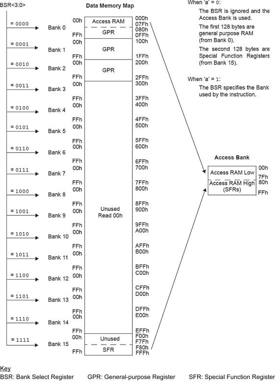
While the lower three banks of data memory are used for general-purpose RAM, the SFRs are contained in a block at the top end of the memory, in the upper half of the top bank. They are shown in Figure 13.5. Note that the four columns shown are not themselves memory banks. In fact, taken together they only form part of the highest bank, as already seen in Figure 13.4.

13.4.2 Access Random Access Memory
We have already come across mentions of ‘Access RAM’ while looking at the instruction set. Figure 13.4 shows two areas of memory that carry this name. These are the lowest and highest 128 bytes of memory. The lowest is general-purpose RAM, while the highest contains all the SFRs. The Access RAM concept provides a way of addressing a part of RAM quickly. While the two halves of Access RAM are at opposite ends of the memory map, when used as Access RAM they are treated as one continuous block of memory. The bits of the BSR are ignored and they then have just an 8-bit address, with the SFR addresses following directly on from the lower Access RAM addresses.
Access RAM is available to all instructions which have the a operand, as seen in Appendix 5 or Table 13.2. If a is set to 0, then only Access RAM is available and it is accessed as described above.
13.4.3 Indirect addressing and accessing tables in data memory
The idea of indirect addressing in the 16 Series was introduced in Section 5.12. This described how a File Select Register (FSR) can be used to hold an address. If the program addresses the (virtual) register INDF, then the address placed in the FSR is used as the address for that instruction.
This concept continues to apply in the 18 Series, but is extended to match the larger memory sizes involved, and with multiple FSR and INDF registers. To begin with, there are now three FSRs, which appear in Figure 13.2. Because of the much larger data memory size, each one needs to have 12 bits. They are therefore each made up of two memory locations and with care can be found in the SFR map of Figure 13.5, as FSR2H:FSR2L, FSR1H:FSR1L and FSR0H:FSR0L.
To further complicate matters, there are five equivalents to the INDF register. These are shown in Table 13.3. They can also be found in the SFR map of Figure 13.5.
TABLE 13.3 ‘Virtual’ registers used in indirect addressing
| ‘Virtual’ register addressed n = 0, 1 or 2 | Action following instruction invoking FSR |
|---|---|
| INDFn | No change to FSRn |
| POSTINCn | The FSR is automatically incremented following access |
| POSTDECn | The FSR is automatically decremented following access |
| PREINCn | The FSR is automatically incremented preceding access |
| PLUSWn | The value in WREG is added to FSRn, to form indirect address. Neither FSR nor WREG is changed |
Now if an instruction addresses any of the locations shown in Table 13.3, then the 12-bit number held in the corresponding FSR is used as an indirect address, accessing a location in the data memory upon which the instruction operates. During instruction execution the value of the FSR is modified as shown.
Does all this sound complicated? Don't worry; you shouldn't have to apply the above knowledge directly. The C compiler will look after these complexities and provide you with a powerful programming tool in a usable form.
13.5 Program memory
13.5.1 The program memory map
The program memory map for all 18FXX20 microcontrollers is shown in Figure 13.6. It can be seen that implemented memory occupies only a modest proportion of the overall capacity offered by the 21-bit bus. Each memory location has a size of one byte. With the normal instruction word being 16 bits, each instruction therefore takes two or four bytes. The less significant byte is stored in a location with an even address. The reset vector, where the program starts, is shown as memory location 0000, and the two interrupt vectors at locations 0008H and 0018H. Interrupt Service Routines (ISRs) must be written to start at one of these locations.

13.5.2 The Program Counter
The Program Counter, seen at the top of Figure 13.6, is 21 bits wide. With each instruction stored as two or four bytes, the Program Counter increments twice, or four times, every instruction.
Access to the Program Counter is available through SFRs in the memory map. The least significant byte is called PCL. It is readable and writeable, and can be seen as memory location FF9H in Figure 13.5. The middle program counter byte, and the higher five bits, are not directly readable or writeable. Updates to these may, however, be made through the PCLATH and PCLATU registers, seen in both Figures 13.2 and 13.5. The contents of these locations are transferred to the Program Counter by any operation that writes to PCL. Similarly, any operation that reads PCL will cause the relevant higher bits of the Program Counter to be transferred to PCLATH and PCLATU.
13.5.3 Upgrading from the 16 Series and computed goto instructions
With the 16 Series, we used the computed goto as a means of retrieving data from a look-up table, as we did for example in Figure 5.9 or Program Example 5.8. An offset was added to the Program Counter to cause a jump to one of a list of retlw instructions. That instruction then caused a return to the main program, with the selected byte of data carried in the W register. This is still possible in the 18 Series, but it is important to remember that each instruction now takes two bytes in program memory. Therefore, any offset added to the Program Counter in a 16 Series program must be doubled to create the same effect in an 18 Series program. An example of how to do this is given in Ref. 13.2.
13.5.4 The Configuration registers
Whereas the 16 Series microcontrollers have a single 14-bit Configuration Word, the 18 Series has a whole set of Configuration registers, reflecting the greater complexity and flexibility of the device. The registers are shown in Table 13.4 and a summary of the function of each bit in Table 13.5. It is easy to see that the usual features – oscillator settings, Watchdog Timer, power-up timing, Brown-out Reset and code protection – are there. Most of these have grown in the options they offer. There are now, for example, 12 oscillator settings, more Watchdog options and more brown-out settings. More bits are therefore needed.
TABLE 13.4 18FXX20 Configuration registers and device identifications
 |
TABLE 13.5 18 Series Configuration Words: 18FXX20 summary of configuration bits and device identifications
| Configuration bit(s) | Summary of function (unprogrammed value is 1, active (enabled) value generally 0) |
|---|---|
| IESO | Internal/External Oscillator Switchover bit |
| FCMEN | Fail-Safe Clock Monitor Enable bit |
| FOSC3:FOSC0 | Selects one of 12 oscillator modes (see Table 12.6) |
| BORV1, BORV0 | Selects Brown-out Reset voltage |
| BOREN1, BOREN0 | Selects Brown-out mode |
| PWRTEN | Power-up Timer Enable bit |
| WDTPS3:WDTPS0 | Watchdog Timer Postscale bits, eight values from 1:1 to 1:32 768 |
| WDTEN | Watchdog Timer Enable bit |
| MCLRE | MCLR Pin Enable bit |
| LPT1OSC | Low-Power Timer 1 Oscillator Enable bit |
| PBADEN | PORTB A/D Enable bit |
| CCP2MX | CCP2 Multiplex, selects RC1 (1) or RB3 (0) |
| DEBUG | Background Debug Enable bit |
| XINST | Extended Instruction Set Enable bit |
| LVP | Low-Voltage Program Enable bit |
| STVREN | Stack Full/Underflow Reset Enable bit |
| CP3:CP0 | Code Protection bits |
| CPD | Data EEPROM Code Protection bit |
| CPB | Boot Block Code Protection bit |
| WRT3:WRT0 | Program Memory Write Protection bits |
| WRTD | Data EEPROM Write Protection bit |
| WRTB | Boot Block Write Protection bit |
| WRTC | Configuration Register Write Protection bit |
| EBTR3:EBTR0 | Table Read Protection bits |
| EBTRB | Boot Block Table Read Protection bit |
| DEV2:DEV0 | Device ID bits: 000 = 18F2520, 010 = 18F2420, 100 = 18F4520, 110 = 18F4420 |
| REV4:REV0 | Revision ID bits |
| DEV10:DEV3 | Further Device ID bits |
The Configuration registers are mapped in program memory starting at memory location 300000H. Like program memory, they are 8-bit locations. The two device identification registers, DEVID1 and DEVID2, are readable only and contain pre-programming information identifying the device and its revision number.
13.6 The Stacks
The Stack in an advanced microprocessor is a versatile memory block, which can be used both automatically – say, for saving a return address in a subroutine call – as well as by the programmer, for short-term data storage. Indeed, in many cases multiple Stacks are used. The 16 Series Stack seen earlier was, however, a small and mechanistic structure. With only eight levels, it is linked directly to the Program Counter, and just saves or returns its value under certain subroutine call or interrupt conditions.
The 18 Series Stack moves some way to taking on the features of the larger microprocessor. The automatic functions remain, for subroutine call and so on, but there is also some user access. There is also limited stacking, in another memory area, of key data registers.
13.6.1 Automatic Stack operations
The main Stack is called, in the 18 Series, the ‘Return Address Stack’. This distinguishes it from the other smaller Stack locations that also exist. It is seen as part of Figure 13.6. It consists of 31 Read/Write memory locations, each of 21 bits. This figure also shows the Assembler mnemonics of those instructions that cause automatic access to the stack. All of these relate to subroutine call or return, with the exception of retfie, the return from interrupt instruction.
13.6.2 Programmer access to the Stack
Not shown in Figure 13.6 is the Stack Pointer, which holds the current Stack address. It is set to zero on all resets and its value is changed by all automatic Stack accesses. Thus, it is incremented when a value is pushed onto the Stack and decremented when a value is popped off. It is also configured as part of an SFR, called STKPTR. As with all SFRs, this is readable and writeable by the programmer. STKPTR is seen as memory location FFCH in Figure 13.5. The five lower bits of STKPTR form the Stack Pointer. The register also contains bits that flag Stack overflow or underflow – respectively STKOVF (also called STKFUL, bit 7) and STKUNF (bit 6).
The value held in the top location of the Stack is accessible to the programmer, and is both readable and writeable. Being 21 bits, it occupies three register locations, TOSU, TOSH and TOSL. These can again be seen in the register map of Figure 13.5, above STKPTR. The instructions push and pop allow the programmer respectively to push the current Program Counter value onto the Stack, or to simply discard the top of the stack, adjusting the Stack Pointer in each case. These are made available primarily to allow the user to set up and manage a software stack.
13.6.3 The Fast Register Stack
The 18 Series structure provides not only a Stack for the Program Counter, but also (in primitive form) a separate ‘Stack’ for the STATUS, WREG and BSR registers. These are single memory locations, not directly accessible to the programmer, which together are called the ‘Fast Register Stack’. When any interrupt occurs the values of the three registers listed are saved. The stacked values are returned if a ‘fast’ return from interrupt is selected. In other words, the retfie instruction should be used with the s operand set to 1. Section 13.7.7 returns to this issue.
The Fast Register Stack can also be used with subroutine calls and returns. As Appendix 5 shows, both call and return instructions can be used with the s bit set, invoking use of the Fast Register Stack. It is of course only safe to do this if interrupts are not being used. Otherwise, an interrupt occurring during a subroutine will cause the Fast Register Stack to be overwritten.
13.7 The interrupts
The 18 Series microcontrollers offer a sophisticated interrupt structure that shows considerable advance over its 16 Series predecessors. Improvements include the introduction of a second interrupt vector, allowing high- and low-priority vectors. This has already been seen in the program memory map of Figure 13.6. All interrupts but one can be allocated to high or low priority. There are more external interrupts, and the possibility of automatic context saving by use of the Fast Register Stack, described in the previous section.
13.7.1 An interrupt structure overview
The interrupt structure is shown in Figure 13.7. Compared to Figure 6.2, where we first met interrupts, it is fairly complex. An understanding of it will, however, lead to effective use of the microcontroller interrupts. Interrupt sources tend to appear from the left of the diagram. The three major outputs are to the right. Two of these lead to the interrupt vectors. Activation of either of these outputs causes a CPU interrupt, with an Interrupt Service Routine (ISR) starting at one or other of the interrupt vectors seen in Figure 13.6. There is also a ‘Wake-up’ output, implemented if in Sleep mode.
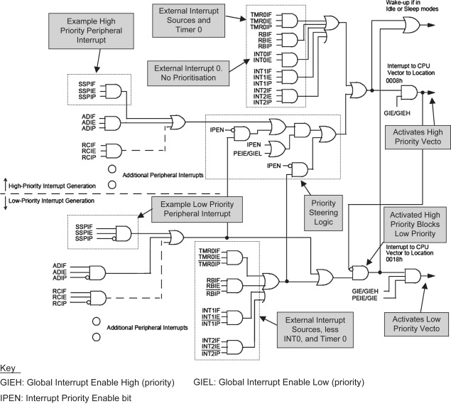
13.7.2 The interrupt sources, their enabling and prioritisation
Let us start by identifying some of the interrupt sources. A useful first block to look at has been labelled ‘External interrupt sources and Timer 0’. This block contains five AND gates, with all but one having three inputs. Look at the top one, with inputs labelled TMR0IF, TMR0IE and TMR0IP. This is the Timer 0 input and it displays a pattern that is repeated many times over. The input …IF is the Interrupt Flag bit, set if the Timer 0 interrupt has occurred; the input …IE is the Enable bit, a bit in an SFR which can be set or cleared by the program. The input …IP is the Priority bit, also in an SFR and set or cleared by the program. If all these inputs are high – i.e. the interrupt is enabled, it is selected as high priority and the interrupt flag has been set – then the output of the AND gate goes high and the interrupt is routed through to the next stage of gating. Notice that the outputs of all AND gates in this block are ORed together.
The block just described is repeated towards the bottom of the diagram. Now, however, the third input to the Timer 0 AND gate is TMR0IP. It is possible to see that every interrupt source (except one, which we will mention below) appears once in the top half of the diagram and once in the bottom. In the top half, it is enabled if its priority bit is high; in the bottom half, it is enabled if the bit is low. Again, the outputs of all AND gates in this block are ORed together.
The one source that is not prioritised is the External Interrupt 0. This is always high priority and is labelled as such in the diagram.
The interrupts from the microcontroller peripherals, towards the left of the diagram, follow a similar pattern to the external interrupts. Again, they can be selected for high or low priority. They are not all shown, as there are so many. Three examples of high-priority sources appear towards the top left of the diagram, and are repeated for low priority towards the bottom left. As before, the logic ensures that for any one interrupt source, either high priority or low priority can be selected. Again, the outputs of all AND gates in each block are ORed together.
13.7.3 Overall interrupt prioritisation enabling
While we have seen that it is possible to prioritise individual interrupt sources, we may not want to do this. Therefore, it is possible to enable or disable the whole prioritisation process. This is done by IPEN, the Interrupt Priority Enable bit. IPEN is the MSB of RCON, a register devoted mainly to recording recent reset events. It appears in part in Figure 13.14.
Look now at the block towards the centre of Figure 13.7, labelled ‘priority steering logic’. The line IPEN appears three times in this block. If it is low, then interrupts from the lower half of the diagram, coming either from peripheral sources or from external sources, are routed up to the upper half of the diagram through the two AND gates in the block. All interrupts in this case are routed through to the high-priority vector and there is no effective prioritisation. There is one more piece of enabling in this state, which we return to soon. When IPEN is low, as just described, the interrupt system is compatible with the 16 Series, although with a different vector address.
If IPEN is high, then high-priority and low-priority interrupts are each routed towards their own vector. Interrupt prioritisation is enabled and individual interrupt sources can be placed in the low- or high-priority domain, with their individual priority control bits.
13.7.4 Global enabling
There are two levels of global interrupt enabling, controlled by bits GIE/GIEH and PEIE/GIEL. These have a somewhat dual function, depending on the state of IPEN – hence the dual nature of their names.
It can be seen that GIE/GIEH controls both of the AND gates leading to the interrupt vectors. Through this it plays its ‘global interrupt enable’ role. If GIE/GIEH is low, there will be no interrupt, whatever the state of IPEN. When IPEN is low, all interrupts are routed towards the high interrupt vector, so it genuinely acts as a ‘global enable’. When IPEN is high, it still has the power to disable both high- and low-priority interrupts. However, it cannot on its own enable the low-priority one, as PEIE/GIEL is also involved. Therefore, it acts as enable for only the high-priority path.
When IPEN is low, PEIE/GIEL acts as an enable line for all unmasked peripheral interrupts. It performs this function through the OR gate at the centre of the ‘priority steering logic’. When IPEN is high, it acts as ‘global enable’ for the lower-priority inputs, through its connection to the output AND gate for the lower-priority vector. Interrupt enabling and prioritisation are explored in Programming Exercise 13.3.
13.7.5 Other aspects of the interrupt logic
Two final elements in this circuit are the line going from the high-priority interrupt output down to the lower-priority control logic. We can see that the action of this is that if a high-priority interrupt is asserted, then the low-priority path is blocked. The reverse is not true, however, and a high-priority interrupt can interrupt a low-priority interrupt. There are also lines from either interrupt path up to an OR gate which leads to Wake-up from Sleep. The action of these lines is independent of the state of the two ‘global enable’ lines.
13.7.6 The Interrupt registers
With the formidable number of bits seen in Figure 13.7, it is clear that a good number of registers will be needed to hold them all. Each interrupt source but one now needs a Flag bit, an Enable bit and a Priority bit, and all the control bits are needed as well. Beyond this, there is further control over some inputs, for example setting the active edge on external interrupts.
The design approach in creating the Interrupt registers has been to retain as far as possible those registers that are used in the 16 Series. This allows a comparatively easy upgrade path for the system designer. Therefore, the 16F87XA INTCON register, appearing in Figure 7.11, is almost exactly replicated in the 18 Series INTCON register, seen in Figure 13.8. Some small retitling of bits has taken place, and the role of GIE and PEIE has been extended, as just discussed.
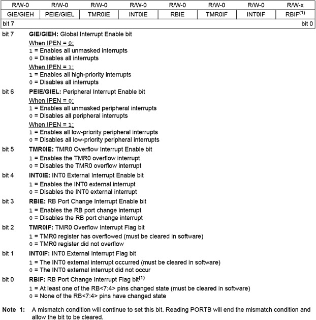
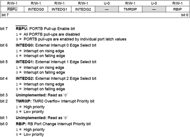
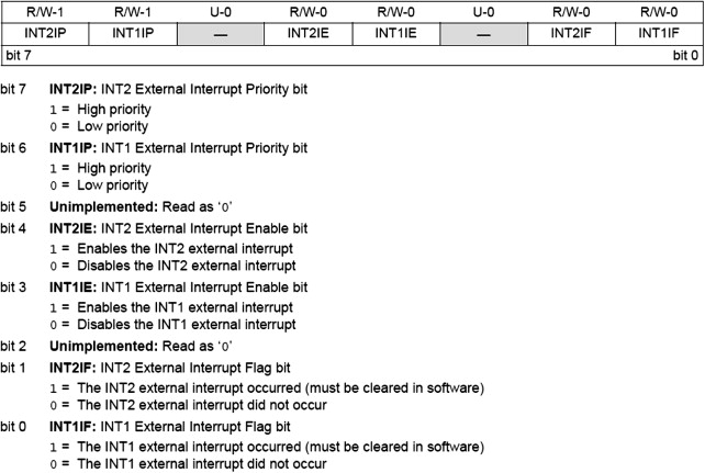
To the INTCON register are added two further Interrupt control registers, INTCON2 and INTCON3. These are shown in Figures 13.9 and 13.10 respectively. They contain the control bits for the interrupts that appear in the INTCON register. The bits are self-explanatory. It can be seen that the ‘odd one out’ is RBPU, which is not an interrupt bit at all, but controls the Port B pull-ups. In the 16 Series it was placed in the Option register, which does not exist in the 18 Series.
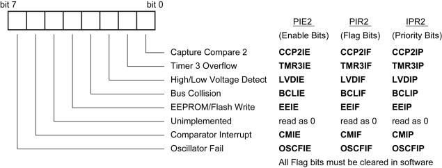
Enable bits, Flag (or ‘Request’) bits and Priority bits for the peripheral interrupt sources are placed in the PIE1, PIE2, PIR1, PIR2, IPR1 and IPR2 registers. These are summarised in Figures 13.11 and 13.12 Again, to improve upward compatibility, they are very similar to the 16 Series registers of the same names, excluding of course the priority registers. It is interesting to compare them, by looking back at Figures 7.12 and 7.13. By doing this, you can see which interrupts have been added, for example Timer 3 and High/Low Voltage Detect. Further details on the operation of some individual peripheral interrupts are given in the sections on those peripherals, later in this chapter.
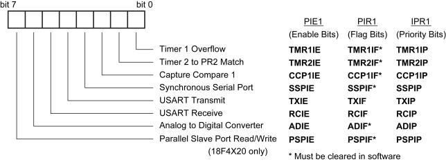
Figure 13.11 18FXX20 PIE1/PIR1/IPR1 (Peripheral Interrupt Enable/Peripheral Interrupt Request/Peripheral Interrupt Priority) registers
13.7.7 Context saving with interrupts
With the Fast Register Stack, described in Section 13.6.3, context saving can in some circumstances be delightfully easy. The programmer must decide first if the three registers saved on this stack, WREG, STATUS and BSR, are adequate for the purpose. If not, or if the fast return from interrupt is not used, then the programmer will need to write code to save all necessary registers at the start of the ISR and retrieve them at the end (as demonstrated in Program Example 6.4). It is important also to remember that a high-priority interrupt can interrupt one of lower priority. In so doing, the interrupt of high priority would overwrite the contents of the Fast Register Stack, and the low-priority interrupt lose its context! In such cases it is not safe to use the Fast Register Stack for low-priority interrupts; context for these should be saved in the software. These issues are explored in Programming Exercises 13.4 and 13.5.
13.8 Power supply and reset
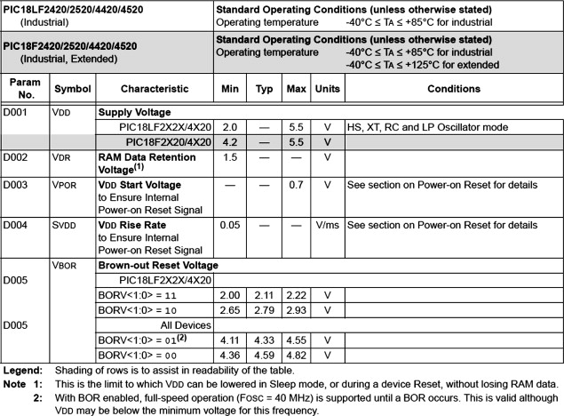
13.8.1 Power supply
The supply voltage requirements of the 18LFXX20 and the 18FXX20 are shown in Figure 13.13. This shows that the 18LFXX20 devices can operate with a supply from 2.0 to 5.5 V, and the 18FXX20 from 4.2 to 5.5 V. The low-power device cannot, however, run at full speed at the lower voltage. The data [Ref. 13.1] shows that its maximum clock frequency at minimum supply voltage is 4 MHz. This rises to 40 MHz at 4.2 V.
13.8.2 Power-up and reset
In Section 2.8 of Chapter 2 we explored the reset circuitry of a simple PIC microcontroller, the 16F84A. The 18FXX20 controllers have a reset structure built directly on the model of Figure 2.10, with just a few extra sources of reset. These are Stack over- or under-flow, Brown-out (already seen in the 16F873A) and use of the instruction reset.
Besides adding further sources of reset, the 18 Series goes beyond this in an interesting way, by providing some history of what the source of reset was. Therefore, coming out of the Reset condition is not the completely fresh start that it is with simple microcontrollers. Now we can find out why we were forced into reset. In certain circumstances this can be very valuable, say if the Watchdog Timer has timed out. This information is provided through the RCON register, whose bits indicate what type of reset has occurred most recently. We have already met RCON, as its MSB is the interrupt IPEN bit.
A listing of all 18FXX20 resets is given in Figure 13.14. This also shows the value of the Program Counter, the RCON register bits and the two Stack overflow bits after the reset has occurred. Now at the restart of a program it is possible to test the state of RCON, with the chance of introducing customised action if a particular type of reset has occurred.
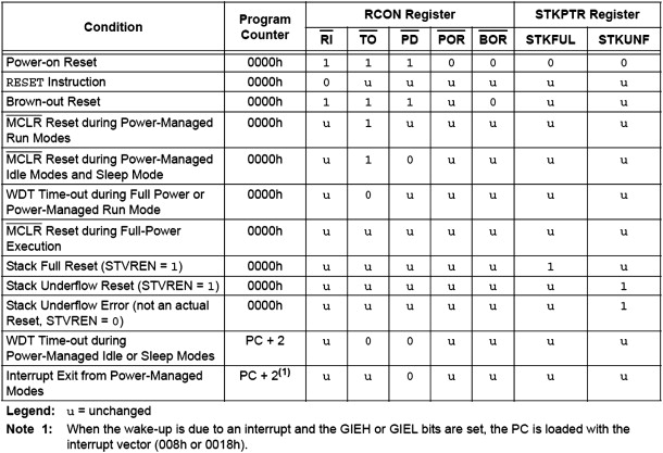
The Software Reset indicated in Figure 13.14 is caused by execution of the instruction reset (Table A5.1). This replicates an external reset caused by a Logic 0 on input MCLR. The outline conditions to ensure Power-on Reset are given in Figure 13.13, along with the different possible settings for the Brown-out Reset.
13.9 The oscillator sources
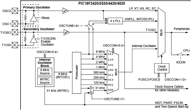
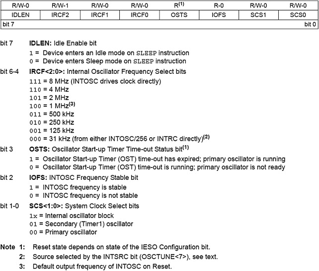
The clock sources and selection possibilities of the 18F2420 are shown in Figure 13.15. This extends the concepts already introduced in Section 12.5 and Figure 12.6. Important developments are the addition of a phase-locked loop (PLL) and Idle modes. Clocking options are summarised in Table 13.6. Oscillator selection is under the control of configuration bits (Table 13.4) and an OSCCON register, seen in Figure 13.16.
| Mode | Description | Config. bits FOSC3:FOSC0 |
|---|---|---|
| LP | Low-power crystal | 0000 |
| XT | Crystal/resonator | 0001 |
| HS | High-speed crystal/resonator | 0010 |
| RC | External resistor/capacitor, Fosc/4 output on OSC2 | 0011 |
| EC | External clock, CLKO function on OSC2 | 0100 |
| ECIO | External clock with OSC2 configured as RA6 | 0101 |
| HSPLL | High-speed crystal/resonator with phase-locked loop | 0110 |
| RCIO | External resistor/capacitor with OSC2 configured as RA6 | 0111 |
| INTIO2 | Internal oscillator block, port function on RA6 and RA7 | 1000 |
| INTIO1 | Internal oscillator block, Fosc/4 output on OSC2; port function on RA7 | 1001 |
| RC | External RC oscillator, CLKO function on OSC2 | 101x |
| RC | External RC oscillator, CLKO function on OSC2 | 11xx |
13.9.1 HSPLL oscillator mode
A phase-locked loop is a clever piece of analog and digital circuitry that can be used, among other things, to multiply by an integer number the frequency of a signal. PLLs are finding increasing usage in microcontrollers to manipulate the frequency of clock signals. This can allow certain sections of the microcontroller to run faster than others, or to run the microcontroller at a clock frequency faster than the oscillator itself. The 18FXX20 PLL can be enabled if the microcontroller is set in HSPLL mode, and then multiplies the oscillator signal (or internal oscillator) by a factor of four. Therefore, for example, the oscillator can run at 10 MHz, but with the PLL running the internal clock frequency will be 40 MHz. This can have the effect of reducing external electromagnetic interference.
13.9.2 Power-managed modes
The 18FXX20 microcontrollers embrace the nanoWatt technology concept, introduced in Section 12.4. Many of their low-power features fall under the title of power-managed modes, neatly summarised in Table 13.7. The last three of these modes are ‘Idle’ modes, where the CPU is switched off but the peripherals allowed to run.
TABLE 13.7 Power-managed modes
 |
An Idle mode is entered by presetting the Idle Enable bit IDLEN in the OSCCON register, and then executing the sleep instruction. The IDLEN bit effectively controls connection of the oscillator to the CPU, as seen to the right of Figure 13.15. In Idle mode all peripherals can continue running, retaining the clock source which was in use before entering sleep. The different Idle modes correspond to the different clock sources available. Exit from Idle mode is generally the same as from sleep, i.e. by enabled interrupt, WDT time-out, or Reset. Running in Idle mode from a slow clock source results in a very striking reduction in power consumption.
It is of course important, when switching between two unsynchronised oscillators of different frequency, to ensure that unwanted glitches do not occur in the clock signal. Therefore, the 18FXX20 contains circuitry to ensure error-free switching and proper transition between the clock sources.
13.10 Introductory programming with the 18F2420
While most programming in this part of the book is to be done with the C language, it is worth simulating some trial programs in Assembler, in order to gain an initial familiarity with the instruction set. If you have followed this book from the beginning, you will be familiar with the MPLAB development environment and the simulator MPSIM. Let us use MPLAB to develop some simple Assembler programs. Review Section 4.5 for a refresher if needed.
13.10.1 Using the MPLAB IDE for the 18 Series
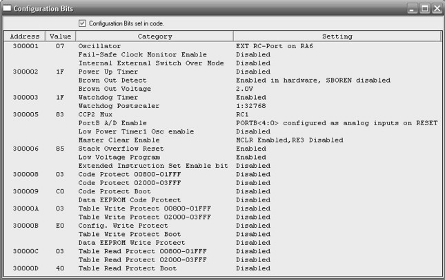
Try opening MPLAB and, using Configure > Select Device, select the 18F2420. See that all familiar development tools remain available. Then, using Configure > Configuration Bits, see the considerably increased number of bits that are available. These were seen in Tables 13.4 and 13.5, and in MPLAB form are shown in Figure 13.17.
13.10.2 The Fibonacci program
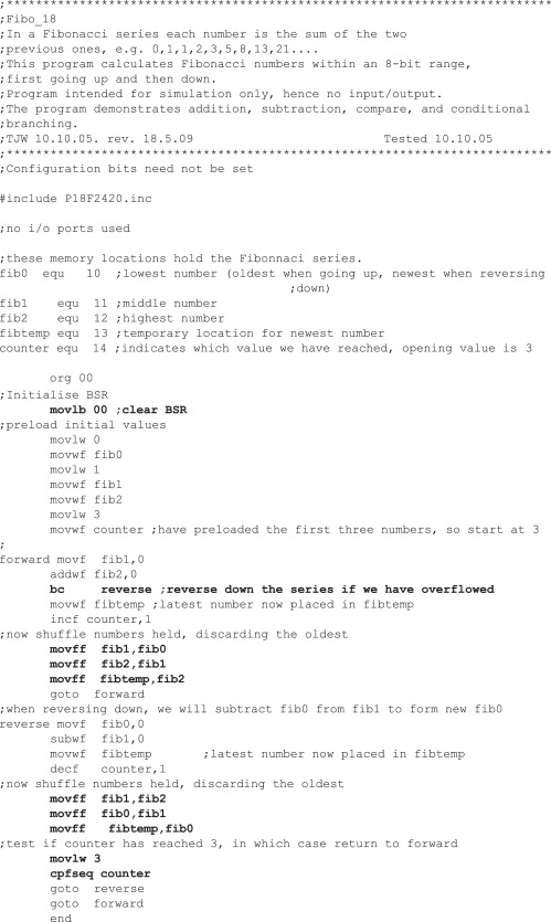
Back in Chapter 5 we met a program that calculates a Fibonacci series, Program Example 5.2. This is not an obvious program for embedded systems, but it allowed us to exercise some simple arithmetic functions in an interesting way on the simulator.
If you continue single-stepping you are likely to find that this version of the program causes an overflow of the 8-bit range. Can you determine the reason and correct it?
Programming Exercise 13.1 shows that an 18 Series device can run using just 16 Series instructions. However, this wastes the powerful new features of the 18 Series CPU. Program Example 13.1 adapts the Fibonacci program in a modest way to the 18 Series, with the changes highlighted in bold. This illustrates use of some of the new instructions. It is worth mentioning that because we are not aiming to go deep into Assembler programming of the 18 Series, the slight complexities of using the Bank Select Register and the Ram Access bit (see Table A5.2) have deliberately been avoided. Indeed, for a simple program like this they are not worth worrying about.
Programming Exercise 13.1
Create a project in MPLAB called Fibonacci-18. Copy into it the source file of Program Example 5.2 from the book’s companion website. Using Configure > Select Device, set the chosen microcontroller to be the 18F2420. You should be able to `build' the program without change or problem. Simulate, using the same Watch window settings as in Programming Exercise 5.2. It should be possible to single-step through the program, initially without any problems. By doing this, you are illustrating that the 18 Series instruction appears to be a super-set of the 16 Series.
Programming Exercise 13.2
From the book's companion website take the source file of Program Example 13.1. Create a project around it and build it. Simulate the program, and use View > Special Function Registers and View > File Registers to view these two areas of memory. Notice how their structure differs from the 16 Series. Scroll the Special Function Registers window to see WREG (address FE8) and PCL (address FF9). Step through the program and see how PCL increments twice for every instruction, as described in Section 13.5.2. Also see the Fibonacci numbers appearing in the data registers.
13.10.3 Applying the interrupts
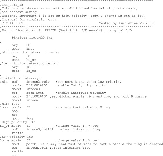
To gain an understanding of the 18F2420 interrupt structure, it is interesting to write and simulate a program which makes use of them. Program Example 13.2 does just this. Read through it carefully, checking how the Interrupt control registers are set up.
Programming Exercise 13.3: Setting up prioritised interrupts
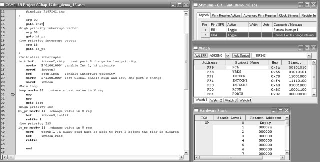
From the book's companion website take the source file of Program Example 13.2. Create a project around it and build it. Set the PORTB A/D Enable bit (PBADEN) configuration bit for digital I/O. Simulate the program with MPLAB SIM. Open a Watch window, and display all SFRs shown in Figure 13.18. Also view the Hardware Stack. Open a stimulus workbook and select RB1 and RB4 as asynchronous inputs. Single-step through the program and see the Interrupt control registers being set up. Once in the loop, force each interrupt in turn. See how the return address (i.e. current program counter + 2) is placed on the Hardware Stack, the interrupt vector address is placed in PCL, and execution moves to the interrupt vector. Observe the reverse process as the ISR comes to an end.
Programming Exercise 13.4: Context saving using the Fast Register Stack
Notice in Program Example 13.2 that the W register is set to a certain value in the main loop and to a different value in each of the ISRs. This is included to illustrate in a simple way the impact that an ISR can have on another section of code. In the simulation set-up described in Programming Exercise 13.3, now try invoking the Fast Register Stack, described in Section 13.6.3, by changing one or both retfie instructions to retfie 1. See now that, if an interrupt is forced, the original context, as represented by the W register value, is retrieved as program execution returns to the main program.
Programming Exercise 13.5: Nested interrupts
Still in the simulation set-up described in Programming Exercise 13.3, try forcing a high-priority interrupt. When in the high-priority ISR, force a low-priority interrupt. The low-priority flag is set, but the high-priority ISR completes before the low-priority one can run. Try now forcing a low-priority interrupt first. Then, within its ISR, force the high-priority interrupt. The low-priority interrupt is itself interrupted and the high-priority ISR runs, before returning to the low-priority, and hence to the main program. Explore the impact and limitations of invoking the Fast Register Stack in each of these scenarios.
13.13 A peripheral review and the parallel ports
The peripherals of the 18FXX20 microcontrollers are summarised in Table 13.1 and seen for the 18F2420/2520 pair in Figure 13.2. When comparing them to the peripherals of the 16F87XA, in Figure 7.2, it can be seen that, in almost every case, the same peripherals appear with the same name and in the same pattern. A difference to note is that the 18 Series controllers claim an extra timer, Timer 3.
Turning to the parallel ports, we find they are very similar to those of the 16 Series, both in structure and interfacing. They each have a PORTX register for data transfer and a TRISX register to set data direction. There is just one significant difference we need to take note of, described now.
When working with a port we may need to do four things: set the data direction, read an input value, set an output value and read back an output value previously written. The 16 Series designs had one weakness in all of this – they were not good at doing the fourth in this list. Suppose a port bit such as the one in Figure 7.15(a) was set to output and a bit value written to it. If the port was then read by the CPU, it was impossible to be certain that the value read was equal to the value previously written. This is because the reading is of the actual port bit pin value. This could be the value output by the bit circuitry or it could be a different value forced by an external device connected to the pin.
To get round this small problem, the 18 Series ports introduce an interesting development. Each port has a third register, LATA for Port A, LATB for Port B and so on, which holds the value of the latched output port bit. This can be read by the program, and the programmer can have complete confidence that he/she is reading the value previously stored at the port and nothing else. The working of the extra data latch register LATA is illustrated in Figure 13.19. This diagram is very similar to its 16 Series equivalent, Figure 7.15(a). With the new register LATA introduced, one expects to see an extra bistable in the circuit somewhere. Interestingly, this is not the case. A quick look at the diagram shows that LATA and PORTA share the same data latch; a write to one is equivalent to a write to the other. The only real difference in the circuit is the LATA buffer appearing at the top of the diagram. A read to LATA activates this buffer and the value held on the PORTA/LATA data latch is transferred to the data bus. Therefore, the LATA is not really a different register at all – but addressing it allows a direct reading of the output of the PORTA data latch.
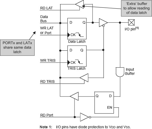
Figure 13.19 Generic 18FXX20 port pin driver circuit (supplementary labels in shaded boxes added by the author)
We will now survey the 18F2420 ports, taking note of this and other small changes.
13.13.1 The 18F2420 Port A
The position of the Port A pins can be seen in the pin layout diagram of Figure 13.1. Unsurprisingly, the pattern is almost the same as the 16F873A, with the digital I/O features of the port being shared with the ADC (analog-to-digital converter) inputs, comparator outputs and a few other features. The Timer 0 input is shared with bit 4 of the Port, which has an Open Drain output. There is the possibility of extra port bits, RA6 and RA7, if certain of the oscillator modes are used, as described in Section 13.9. The three registers associated with Port A – PORTA, TRISA and LATA – can be seen in the fourth column of the register map (Figure 13.5).
13.13.2 The 18F2420 Port B
The position of the Port B pins can be seen in the pin layout diagram of Figure 13.1 and its three primary registers – PORTB, TRISB and LATB – in Figure 13.5. LATB plays an identical function to LATA, discussed above.
The port keeps most of the characteristics of the 16 Series, but with significant increase in the number of shared functions, for example with the introduction of more external interrupt sources. Importantly, bits 4–0 come under the control of the PBADEN configuration bit; this determines whether those bits are to be used as analog inputs or normal digital input/output. It can be seen that bits 5–7 share with the in-circuit debug functions of PGD, PGC and PGM, the last of these having moved from its 16 Series position. The three external interrupt inputs share with the lower three bits of the port. An interesting addition is the introduction of an alternative CCP2 connection, on bit 3. This relieves pressure on the very ‘busy’ pin of Port C bit 1, and allows the Timer 1 external oscillator to be used at the same time as CCP2.
Internal pull-ups are still available on all pins, with the controlling bit, RBPU, now placed in register INTCON2 (Figure 13.9). The interrupt on change function, whereby a change on any of pins 4–7 causes an interrupt flag to be set, is also in place. The Enable and Flag bits, RBIE and RBIF, are in the INTCON register (Figure 13.8).
13.13.3 The 18FXX20 Ports C and E
As with the other ports, the position of the Port C pins can be seen in the pin layout diagram of Figure 13.1 and that of its three primary registers – PORTC, TRISC and LATC – in Figure 13.5. As with the 16F87XA, this port shares its pins with the serial ports and the CCP functions, while bit 0 is shared with the Timer 1 input. This bit and bit 1 can also be used for an external oscillator input for Timer 1. Because of these shared functions, the port pin driver circuits are comparatively complex. The pin function can, moreover, be taken over by peripheral functions – care is therefore needed. This override does not, however, include the reading of the LATC register. This can be read whatever mode a port pin is operating in.
Finally, notice that one bit of Port E is squeezed onto the 18F2420, on pin 1, if MCLR is disabled. This can only be done through the MCLRE configuration bit, seen in Tables 13.4 and 13.5. You then get bit 3 of Port E. This is input only, so no TRISE or LATE bits are provided.
13.14 The timers
All versions of the 18FXX20 have no less than four programmable timers, as well as a Watchdog Timer. We will survey the timers in turn, making extensive use of information already provided for their 16 Series equivalents.
13.14.1 Timer 0
The 18FXX20 Timer 0 draws its roots clearly from the 16 Series Timer 0. It can, however, operate either in 8-bit or in 16-bit mode. In 8-bit mode the action of Timer 0 is effectively the same as the 16 Series Timer 0 of Figure 6.8. Unlike the 16 Series Timer 0, which shares its prescaler with the WDT, the prescaler is entirely assigned to the timer.
In 16-bit mode the action of the timer is as shown in Figure 13.20. The lower byte of the counter itself is called TMR0L, while the higher byte is simply called TMR0, as it is the same register location as the 8-bit version.
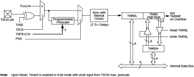
An interesting problem occurs in 16-bit timers when operating in the 8-bit environment. Suppose the program needs to read the value held in the timer. The two bytes are read in turn. It is possible, however, that an increment occurs after the first byte has been read, maybe causing an overflow from lower to higher byte. The value of the two bytes that have been read can therefore be seriously in error.
The solution to this problem is seen in Figure 13.20. A buffer, TMR0H, is included alongside the timer higher byte, TMR0. It is impossible to access the higher byte directly. Whenever the lower byte is read, however, the value of TMR0 is simultaneously transferred to TMR0H. This can be read in a later instruction. Its value is guaranteed to correspond exactly to the value of the lower byte when it was read. Similarly, if the programmer wishes to write to the timer, the program should first write the required higher byte to TMR0H. When the lower byte is written to TMR0L, then the value stored in TMR0H is transferred simultaneously to TMR0. Again, the 16-bit value being loaded into the timer is guaranteed to be correct, and uncorrupted by increments occurring within a two-byte transfer.
In either mode of Timer 0, an interrupt is generated when the counter overflows from its maximum value (FFH for the 8-bit and FFFFH for the 16-bit). The same bit, TMR0IF, seen in Figure 13.7, is used for both interrupts.
Timer 0, in 16-bit mode and with interrupt, is used in a number of the C example programs in later chapters.
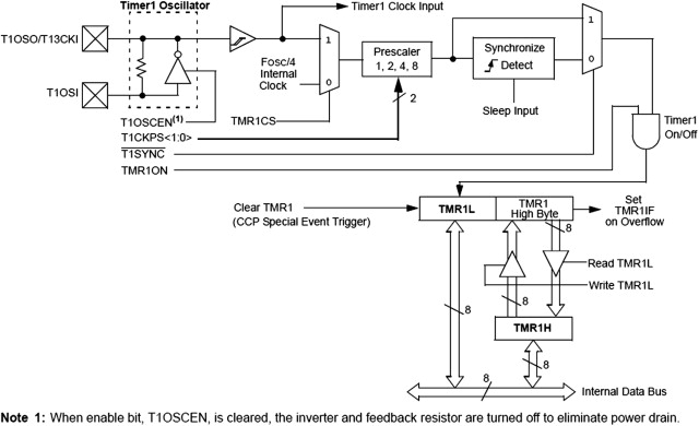
13.14.2 Timers 1 and 2
The 18FXX20 Timer 1 in its basic form is nearly identical to the 16 Series Timer 1, as seen in Figure 9.1. However, as the clock source diagram of Figure 13.15 shows, its oscillator can now be selected as the microcontroller clock source. The timer is also now equipped with the ‘16-bit Read/Write’ mode. This is just as described for Timer 0 and when enabled operates as shown in Figure 13.21. There is now a buffer register TMR1H for the higher byte, allowing synchronised data transfer to or from the timer. A small further difference with the 16 Series Timer 1 is the ability to clear the timer through a ‘special event’ from the CCP module. This is also seen in Figure 13.21 and is described in Section 13.15.
The 18F2420 Timer 2 is the same as the 16 Series Timer 2, shown in Figure 9.4. Similarly, it has a control register T2CON, the same as in Figure 9.5.
13.14.3 Timer 3
Timer 3 is structurally the same as Timer 1, so is easy to understand. It is shown in its basic form in Figure 13.22. As with Timer 1, this one can be operated as a timer with internal clock source input, as a counter with external input or as a timer with external oscillator input. For the last two, inputs are shared with Timer 1. Thus, if an external oscillator is used, it is that of Timer 1, which must be enabled with the T1OSCEN bit in T1CON. If external input is used, it is the same input as Timer 1, i.e. pin 11 in the case of the 18F2X20.
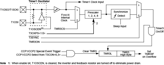
Like Timers 0 and 1, Timer 3 also has a ‘16-bit Read/Write’ mode. Figure 13.22 shows the timer when this mode is not selected. If it is selected, the timer's interface with the data bus takes the form shown in Figure 13.21. Reading or writing to the higher byte is then buffered, with the buffer being memory mapped as TMR3H.
We will see that the timer can be linked to a CCP (capture/compare/PWM) module and used for capture and compare instead of, or alongside, Timer 1. The ‘CCP special trigger’ is seen coming in to Figure 13.22, as a possible source of reset for the timer. These functions are described further in Section 13.15.
13.14.4 The Watchdog Timer
The Watchdog Timer (WDT) is identical in concept to the 16 Series WDT, as described in Section 6.5. It is a free-running counter which, if enabled and allowed to time out, will cause the microcontroller to be reset. It is enabled by the WDTEN configuration bit (Table 13.4). It has its own dedicated postscaler (unlike the 16 Series, where it is shared with Timer 0), whose setting is determined by configuration bits WDTPS3 to WDTPS0. Reference 13.1 indicates that the nominal time-out period is 4 ms, for a postscaler value of 1. If the postscaler is set to 32 768, the nominal time-out value rises to 131 s. Both WDT and postscaler are cleared by execution of the clrwdt instruction. This lengthened timeout duration was recognised in Section 12.4 as an important element of nanoWatt technology.
A further development in the design strategy for the WDT is the inclusion of a software WDT enable bit, SWDTEN. This is the LSB, and the only active bit, in the register WDTCON, seen at memory location FD1H in Figure 13.5. If the WDT has been disabled in the Configuration register, then it can be enabled by setting the SWDTEN bit. If the WDT is enabled in the Configuration register, then the SWDTEN bit has no effect. The ability to switch the WDT on and off goes rather against the whole concept of the WDT – how wise is it to have a safety feature that can be switched off? However, it allows the WDT to be enabled for certain modes of operation and disabled for others. As with all safety or reliability features, it should be used with caution.
13.15 The capture/compare/pulse width modulation modules
The 28-pin 18F2420/2520 microcontrollers have two CCP modules, as seen in Figure 13.2. These are very similar to the 16 Series modules, applying exactly the principles described in Section 9.4.1. The CCP modules work with Timers 1, 2 and 3 to provide capture, compare and PWM operation. An important difference to the 16 Series, and a big step forward in terms of flexibility of operation, lies with the addition of Timer 3 and its interlinking with the CCP modules. The 18F4420/4520 microcontrollers also have two CCP modules, one standard and one enhanced, the latter as described in Section 12.6.3.
13.15.1 Capture mode
The CCP configured for Capture mode is shown in Figure 13.23 This is a direct equivalent of Figure 9.8 and applies the principles described in Section 9.4.2. Both inputs are, however, drawn out here. The major structural difference is that both Timers 1 and 3 are available to be used. This allows two input signals of rather different time characteristics to be ‘captured’. Selection of the timer to be used is determined by the Timer 3 control register, T3CON. Once this selection is made, capture operation is the same as for the 16 Series.

13.15.2 Compare mode
The CCP configured for Compare mode is shown in Figure 13.24. This is a direct equivalent of Figure 9.9 and applies the principles described in Section 9.4.3. As with the Capture mode above, both inputs are drawn out here. The major structural difference, of both Timers 1 and 3 being available, is shown. Selection of the timer to be used is again determined by bits within the T3CON register.
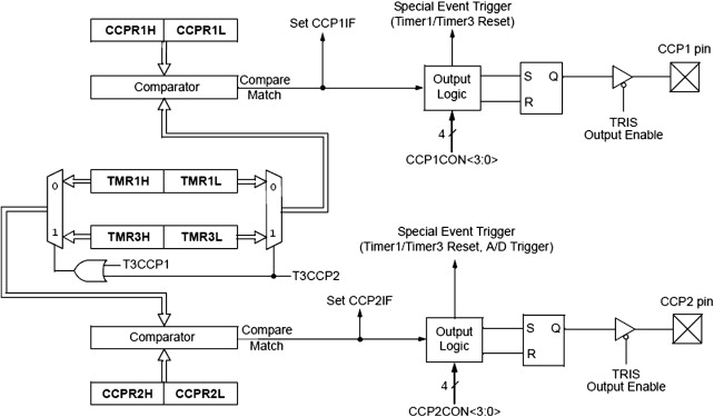
13.15.3 Pulse width modulation
The CCP modules configured for PWM follow the principles described in Section 9.5.1. They behave like the 16 Series module, hence acting as described in Section 9.5.2 and as seen in Figure 9.11.
13.16 The serial ports
The 18FXX20 has two serial modules, the Master Synchronous Serial Port (MSSP) and the Enhanced Addressable Universal Synchronous Asynchronous Receiver Transmitter (EUSART), as seen in Figure 13.2. The MSSP is very similar to the 16 Series peripheral of the same name, with the same SFRs, and can thus be configured either in SPI or I2C mode. The EUSART has already been outlined in Section 12.6.4. Of course the operating environment of the 18 Series is different, so interrupts can be prioritised, peripherals can be kept running in Idle modes, and so on, but all operating principles described in Chapters 10 or 12 continue to apply.
13.17 The analog-to-digital converter
The 18FXX20 ADC module now has an amazing 10 possible inputs for 28-pin versions and 13 for 40- or 44-pin versions. It retains the input model of Figure 11.10, but with the hold capacitor reduced from 120 pF to 25 pF, and the sampling switch resistance also reduced (to around 2 kΩ for a 5 V supply). These reductions lead to significant saving in acquisition time, offering considerably faster overall acquisition and conversion time. Interestingly, the hold capacitor reduction is not as low as the 10 pF quoted for the 16F883, discussed in Section 12.6.5. If we apply these values to the Derbot data acquisition, as we did in Section 11.6, we get, for 10-bit accuracy:
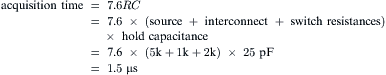
A further development is the ability to introduce automatic delays for acquisition time instead of using software delays, as we did for example in Program Example 11.1. Speed can be further increased because the minimum value for the clock period, TAD, is also reduced. This is dependent on operating conditions, but is 0.7 μs for conditions applied in the Derbot. With changes to the CCP modules, it is also possible to set up a repetitive acquisition sequence with minimal program interaction.
The ADC is controlled by the ADCON0, ADCON1 and ADCON2 registers. While these are the same names as used in the 16F873A, they are not structured the same internally. The conversion result is placed in ADRESL and ADRESH. All these registers can be found in a block in Figure 13.5; the detail of ADCON1 is shown in Figure 13.25.
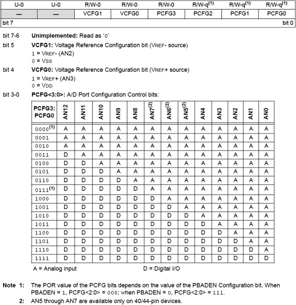
As we will be applying the C programming language soon, we won't need to attend to the details of the control registers, except to note one important difference. While ADCON1 still controls the selection of ADC input channels, it does not follow the pattern of Figure 11.8, and the input combination we have used for the 16F873A in the Derbot is not available. This can be seen in Figure 13.25. Therefore a small change has to be made to the Derbot PCB if the 18F2420 is to be used in the light-seeking program.
13.18 Applying the 18 Series in the Derbot
The Derbot loaded with an 18F2420 microcontroller is used in the chapters that follow for all program examples. To indicate this change of microcontroller, it is called ‘Derbot-18’. A small hardware modification which is implemented is described in Appendix 3.
From a hardware point of view there is little that is done with the 18F2420 that could not have been done with the 16F873A. The big step forward lies in the use of C, which works much better with the 18 Series. This in its turn leads to the use of the real-time operating system; we meet this towards the end of the book.
Summary
• The 18 Series microcontrollers represent a very clear step forward in the PIC design strategy. The CPU and memory structure are radically redeveloped, while many peripherals are retained.
• The standard instruction set is increased to 75 distinct instructions, with big new capabilities in arithmetic, program branching, table access and memory usage.
• Data memory is structured to give a much greater RAM capacity and a separate grouping of Special Function Registers.
• Program memory has greatly increased capacity, with a larger address bus, and the 16-bit instructions are now split into two bytes for storage. The Stack is deeper and more flexible.
• 18 Series microcontrollers adopt the peripherals of the 16 Series, with some upgrades; generally, peripherals are designed to power-up in the mode closest to the 16 Series version.
13.1. PIC18F2420/2520/4420/4520 Data Sheet (2008). Microchip Technology Inc., Document no. DS39631E; www.microchip.com
13.2. Migrating designs from PIC16C74A/74B to PIC18C442, Application Note AN716. Document no. DS00716A. Microchip Technology Inc. 1999.
Questions and exercises
Aim to complete Programming Exercises 13.1 to 13.5 and the questions below.
1. By reading the 18F2420 data sheet, Ref. 13.1, answer the questions below.
2. An embedded systems company estimates that 10% of the instructions in its programs are two-word (e.g. movff). For this proportion, how many instructions can the 18F2420 program memory hold?
3. Although many 18F2420 instructions have a direct equivalent in the 16 Series family, and others do not. The instructions cpseq, movff, negf, subfwb, and tstfsz are ‘new'. Write a macro for each of these, using only 16 Series instructions, so that the same function is performed. Compare the number of instruction cycles each takes to execute and comment on the benefit of the new instruction.
4. Rewrite the opening section of Program Example 13.2, enabling External Interrupt 0 and Timer 0 interrupt on overflow with equal priority. External Interrupt 0 should interrupt on the rising edge.
5. The Interrupt control registers at a certain moment in an 18F2420’s program execution are found to read:
Deduce the interrupt set-up and what the program is doing.
6. A designer wants to use an 18F2420 microcontroller in an application which requires four interrupts. Timer 1 overflow and Low Voltage Detect are to be high priority, and Port B interrupt on change and USART receive are to be low priority. What interrupt-related SFRs need to be preset and to what value?
7. A designer new to the 18 Series microcontrollers is designing an application to run from three nickel metal hydride cells in series. There is no supply regulation, but he wants a means of detecting when the battery voltage has fallen to around 3.5 V, and for the system to then go into a safe shutdown mode. Describe the options, and give your advice on the best solution to this design problem. (Note that access to Ref. 13.1 may be needed.)
8. A certain product has two distinct modes of operation, `user control' and `unattended'. It has been decided that the Watchdog Timer (WDT) should be enabled when unattended, but not enabled if under user control. The program structure in unattended mode is a single continuous loop, whose maximum execution time is 50 ms. Write notes giving design guidance on how the WDT should be implemented, including program action which can be taken if a WDT timeout does occur. (Note that access to Ref. 13.1 may be needed.)