
CHAPTER 11 Data acquisition and manipulation
In the early chapters of this book we limited ourselves to a world that is almost entirely digital. While we want to benefit from the advantages that digital signals can offer us, we need to recognise that most real variables are analog in nature. They are continuously variable and can take an infinite range of different values, whether we are talking about temperature, sound level, frequency or other variables. It is necessary, therefore, for the microcontroller to be able to read values that are analog and if necessary generate output values that are analog, even though internally the microcontroller is relentlessly a digital device. The process of converting an analog signal to digital, along with all the attendant signal manipulation, is usually called ‘data acquisition’.
Once data from the outside world has been acquired, it needs to be processed and put to use. It may also need to be averaged, scaled, linearised or stored. Quite possibly it will be used for some form of control purpose and it may need to be displayed, or transmitted to another device.
Data acquisition, and the use of the data acquired, is the business of this chapter. In the chapter you will learn about:
• The characteristics of the 16F873A analog-to-digital converter.
• How the 16F873A analog-to-digital converter can be applied.
• The use of comparators and the 16F873A comparator capability.
Once we have the ability to acquire data and manipulate it in simple ways, we are in the powerful position of being able to make a variety of measuring devices. The chapter therefore ends with a number of illustrative projects. These use the Derbot either as an AGV or else simply use the core design as the basis for other projects, which have no need for wheels!
11.1 The main idea – analog and digital quantities, their acquisition and use
Most transducers produce output signals that are an analog of the quantity they represent. Thus, the voltage output from a temperature sensor represents the temperature as faithfully as it can, increasing or decreasing as the temperature does. Similarly, a microphone output signal represents the precise characteristics of the sound wave as best it can, in amplitude, frequency and waveform. Analog signals are fine things, but they suffer from a number of big disadvantages, as Table 11.1 shows. Digital signals, on the other hand, as the table indicates, perform better on most counts and with today's technology are easier to work with. In many cases the advantage is dramatic and overwhelming.
TABLE 11.1 Some properties of analog and digital quantities
| Property | Analog | Digital |
|---|---|---|
| Means of (electrical) representation | A continuously variable voltage, or current, represents the variable. | Variable is represented by a binary number. |
| Precision of representation | Can take an infinite range of values; absolute precision is theoretically possible, as long as the signal is kept completely uncorrupted. | Only a fixed number of digit combinations are available to represent measure; for example, an 8-bit number has only 256 different combinations. ‘Continuously variable’ quality of analog signal cannot be replicated. |
| Resistance to signal degradation | Almost inevitably suffers from drift, attenuation, distortion, interference. Cannot completely recover from these. | Digital representation is intrinsically tolerant of most forms of signal degradation. Error checking can also be introduced and with appropriate techniques complete recovery of a corrupted signal can be possible. |
| Processing | Analog signal processing using op amps and other circuits has reached sophisticated levels, but is ultimately limited in flexibility and always suffers from signal degradation. | Fantastically powerful computer-based techniques available. |
| Storage | Genuine analog storage for any length of time is almost impossible. | All major semiconductor memory technologies are digital. |
It is possible fairly readily to convert a signal from analog to digital form, using an Analog-to-Digital Converter (ADC). The circuits available to do this conversion are comparatively complex. Their design is a mature art form, however, and they are available as ready-to-use integrated circuits or modules within a microcontroller.
As embedded designers, we will need to understand the characteristics of the ADC, so that we can choose the right one and use it effectively.
11.2 The data acquisition system
When converting an analog signal to digital form, it is usually not enough just to find a suitable ADC. Usually, more than one input is required and the signal needs processing before it can be converted. In most cases, therefore, it is necessary to build up a complete ‘data acquisition system’. The elements of such a system are shown in Figure 11.1. This shows, in block diagram form, a system with multiple inputs, amplification, filtering, source selection, Sample and Hold, and finally the ADC itself. The different elements are outlined in the sections which follow.

11.2.1 The analog-to-digital converter
The task of the ADC is to determine a digital output number that is the equivalent of its input voltage. The design of such circuits is a non-trivial task. Many very different ADC circuits have been developed, targeted towards different applications. Some, like the dual ramp ADC, are slow but with very high accuracy, and useful for precision measurements such as digital voltmeters. Others, like the Flash converter (not to be confused with Flash memory technology), are fast but of lesser accuracy, and are used to convert high-speed signals such as video or radar. Others, like the successive approximation ADC, are of medium speed and medium accuracy, and useful for general-purpose industrial applications. This is the type most commonly found in embedded systems. Descriptions of how this type of ADC circuit works can be found in most electronics textbooks [see Ref. 1.1].
An ADC is characterised principally by the following features.
Conversion characteristic
The ADC accepts an input voltage that is infinitely variable. It converts this to one of a fixed number of output values. An example ADC conversion characteristic is shown in Figure 11.2, where the input voltage is represented on the horizontal axis and digital output on the vertical. If the ADC is converting continuously and the input voltage is gradually increased from zero, the output is also initially zero. At a certain value of input, the output changes to …001. It stays at this same value as the input increases further, until at another input value the output switches to …010. If the input voltage increases continuously, the output at some point reaches its maximum value. The input has then traversed its full ‘range’. The output will have moved stepwise up to its maximum value. For an n-bit ADC, the maximum output value will be (2n – 1). For example, for an 8-bit ADC, the final value will be (28 – 1), or 11111111B, or 255D.
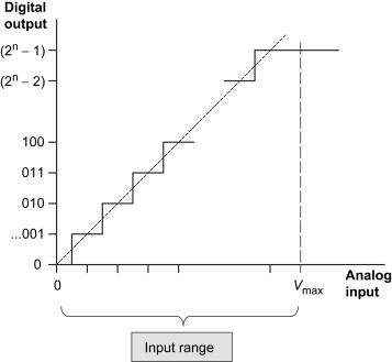
The input range shown in Figure 11.2 starts from zero and goes up to the value Vmax. This is placed a little to the right of where one might expect it, at the centre of where a step for 2n would occur. This positioning allows the horizontal axis to be divided into exactly 2n equal segments, each centred on an output transition.
Many ADCs have a characteristic like that in Figure 11.2, for example with an input range of 0–5 V. Others, however, have a bipolar range, with the input voltage taking both positive and negative values, for example –5 to +5 V. In every case the input range Vr is the difference between maximum input voltage and minimum input voltage. The range usually relates in a direct way to the value of the voltage reference, which forms part of the ADC.
It can be seen intuitively from the diagram that the higher the number of output bits, the higher will be the number of output steps and the finer is the conversion. A measure of the fineness of conversion is called the ‘resolution’. This is the amount by which the input has to change to go from one output value up to the next. In the diagram, the resolution is the width of one step in the conversion characteristic. An ADC with n output bits can take 2n possible output values, from 0 up to 2n – 1. It therefore has a resolution of Vr/2n, where Vr is the input voltage range. An incoming signal should use as much of the input range as possible, without exceeding it. If it only uses a part of it, then the effective resolution is degraded and the ADC is not being put to best use.
Conversion speed
An ADC takes time to do its work. That time is called the conversion time. A slow ADC, with a high conversion time, will only be able to convert low-frequency signals, as Nyquist's criterion (Section 11.2.2) must always be satisfied. The conversion time of an ADC defines which type of signal it can be used to convert. As suggested earlier, high-accuracy ADCs generally take longer to complete a conversion.
Digital interface
The digital interface is made up of the control signals and the data output. Typical control signals are shown in Figure 11.1. Generally, there is a signal to the ADC that causes a conversion to start. When the conversion is complete, the ADC signals that completion with an output signal. A further signal causes the ADC to output its data. Depending on the type of interface required, the ADC has a parallel or serial data interface.
An ADC always works in conjunction with a ‘voltage reference’. This is a device or circuit that maintains a very precise and stable voltage, and is based around a zener diode or a band-gap reference. The ADC effectively uses the voltage reference as the ruler with which it measures the incoming voltage. An ADC is only as good as its voltage reference. For accurate A-to-D conversion, a good ADC must be used with a good reference.
11.2.2 Signal conditioning – amplification and filtering
To make best use of the ADC, the input voltage should traverse as much of its input range as possible, without exceeding it. Yet most signal sources, say a microphone or thermocouple, produce very small voltages. Therefore, in many cases amplification is needed to exploit the range to best effect. Voltage level shifting may also be required, for example if the signal source is bipolar while the ADC input is unipolar (voltage is positive only).
If the signal being converted is periodic, then a fundamental requirement of conversion is that the conversion rate must be at least twice the highest signal frequency. This is known as the Nyquist sampling criterion. If this criterion is not met, then a deeply unpleasant form of signal corruption takes place, known as ‘aliasing’ (see Ref. 1.1 or signal processing text for further details). Anti-aliasing filtering may therefore be required to ensure that the Nyquist criterion is satisfied.
11.2.3 The analog multiplexer
If there are to be multiple inputs, then an analog multiplexer is used. The alternative, of multiple ADCs, is both costly and space-consuming. The multiplexer acts as a selector switch, choosing which input out of several is connected to the ADC at any one instant. The multiplexer is built around a set of semiconductor switches. It is important to know that the semiconductor switch is an imperfect device. In particular, when switched ‘on’, it has internal series resistance, which can range from tens to thousands of ohms. This can impact on the data acquisition process, as we shall see.
11.2.4 Sample and Hold, and acquisition time
Because most ADCs are unable to accurately convert a changing voltage, a ‘Sample and Hold’ (S&H) circuit is often found. This takes a sample of the voltage, like a snapshot, and holds it steady for the duration of the conversion. A circuit of a simple but practical S&H is shown in Figure 11.3. At its heart are just a semiconductor switch and a capacitor. When the switch is closed, the capacitor charges up to the input voltage VS. At this moment, ideally VO = VC = VS, as the buffer amplifier just has unity gain. When the switch opens, the charge is left on the capacitor and VC (and hence VO) remains at a fixed value. In practice there is some leakage from the capacitor, so the output voltage drifts. This circuit is sometimes also called ‘track and hold’, as when the switch is closed the output voltage follows, or tracks, the input.
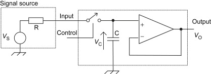
One problem with this simple circuit is that there is inevitably series resistance in the signal path. This is represented by the resistor in the circuit. When the switch closes, therefore, the capacitor voltage VC does not take on the signal voltage immediately, but rises towards it exponentially. This is shown in Figure 11.4. The voltage rise is given by:
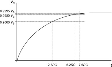
Our interest from a data acquisition point of view is to ensure that the voltage has risen sufficiently close to its final value with the switch closed, before the switch is opened (the signal is then ‘held’) and a conversion allowed to start. The time that VC (and hence VO) takes to reach a value deemed to be acceptable is called the ‘acquisition time’.
Let us suppose that VC must rise to 90 per cent of its final value, VS. Then, substituting into Equation (11.1):

This is shown in Figure 11.4. It is, however, an undemanding requirement. To ensure good accuracy in data conversion, the error introduced by this process should be less than the equivalent of half of one LSB. Hence, for 8-bit conversion, this implies that the acquired voltage value VC must reach ≥ (511/512)VS, or 0.9980VS. For 10-bit conversion it must be ≥ (2047/2048)VS, or 0.9995VS.
Following the calculation above, but substituting in the 10-bit value, we get:
The resulting acquisition times are shown in Figure 11.4. It is clear that acquisition time increases with increasing resistance, capacitance and with accuracy required. We will meet practical application of this calculation later in the chapter.
It is worth noting that the multiplexer circuit and S&H circuit can be merged into one, with the multiplexer switches forming the S&H switch. This is common practice.
11.2.5 Timing and microprocessor control
Usually, a data acquisition system is under the control of a microprocessor or microcontroller. This can control the overall system timing, including which input is being selected, when the selected signal is sampled and when the conversion starts.
The process of a single conversion can be represented as a flow diagram, as shown in Figure 11.5. Two major time requirements need to be satisfied – the acquisition time (of the S&H) and the conversion time (of the ADC).
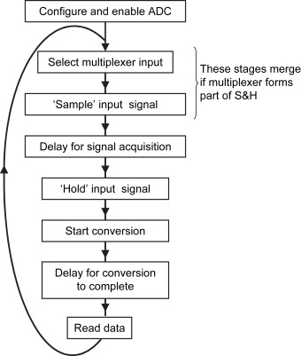
Once the system is initialised, the multiplexer switch can be set. The S&H can then start its sample process. A period equal to or greater than the required S&H acquisition time must elapse. The ADC can then start its conversion. Again, this takes finite time. The ADC flags when it has completed a conversion and the microprocessor can read the output data.
11.2.6 Data acquisition in the microcontroller environment
Embedded systems need ADCs, so it is natural to expect to find an ADC integrated onto a microcontroller as one of its peripherals. It is important, however, to realise that ADCs and microcontrollers do not make happy bedfellows. To operate to a good level of accuracy, an ADC needs a quiet life (electronically speaking), with excellent and clean power supply and ground, and freedom from electromagnetic interference. A microcontroller, on the other hand, being a digital device, tends to corrupt its power supply and ground with a voltage spike on every switching edge. As a consequence, with all its intensive internal digital activity, it radiates a smog of local interference. Therefore, to integrate an ADC onto a microcontroller is at best a compromise and high accuracy is not usually possible.
Despite this, ADCs are widely available in the microcontroller environment, with many microcontrollers having an on-chip ADC. These are mostly 8- or 10-bit.
11.3 The PIC 16F87XA ADC module
11.3.1 Overview and block diagram
The 16F87XA has a versatile and powerful 10-bit ADC module, shown in Figure 11.6. This provides a subset of the overall data acquisition system shown in Figure 11.1, having an ADC, a multiplexer and the possibility of using the supply voltage as the voltage reference. The particular ADC design used incorporates in an interesting way the function of Sample and Hold, discussed further in Section 11.3.3.

Figure 11.6 The 16F87XA analog-to-digital converter (supplementary labels in shaded boxes added by the author)
The input multiplexer, seen to the right of the diagram, has five channels for the 16F873A and ’F876A, and eight for the 16F874A and ’F877A. The inputs are shared with five of the six Port A bits, and three of the eight Port E (for 16F874 and ’F877) bits. Only Port A bit 4 is not used, as it already shares with the important Timer 0 input. Port bits can be allocated in a flexible way to analog or digital input, according to settings in an SFR.
An external voltage reference can be used for applications requiring reasonable accuracy, with terminals for both positive and negative connections provided. Provision of the negative connection means that the reference does not have to be referred to system ground. For lower-cost, lower-accuracy conversions, the power supply voltage can be used as the reference. The input range is equal to whatever voltage reference is chosen.
11.3.2 Controlling the ADC
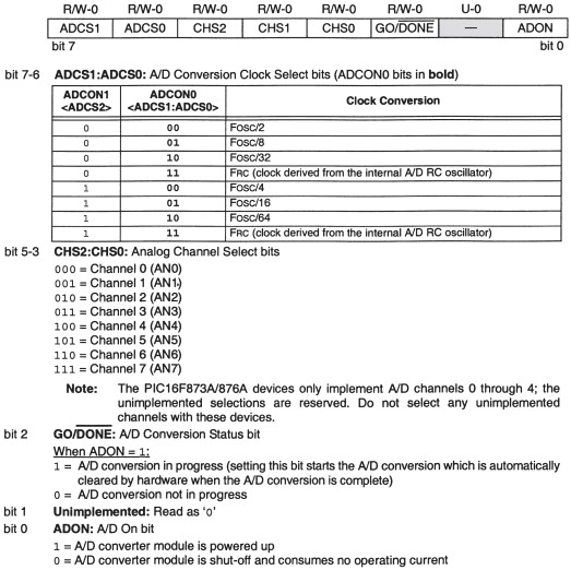
The ADC is controlled by two SFRs, ADCON0 (Figure 11.7) and ADCON1 (Figure 11.8). The result of the conversion is placed in two further SFRs, ADRESH and ADRESL. These four registers can all be seen in Figure 7.6. Other SFRs also have an important impact on the ADC. These include TRISA and (for the 40-pin devices) TRISE. Any bits used for analog input must be set as inputs in these. Registers PIR1 and PIE1, which contain the ADC interrupt flag and interrupt enable bits respectively, are also used.

The control possibilities are now described, in the approximate sequence they would be used.
Switching on
The ADC is switched on and off by the ADON bit of ADCON0. Switching it off when not needed offers a slight power-saving advantage.
Setting the conversion speed
Operation of the 16F87XA ADC is governed by the ADC clock, which has a period TAD. A full 10-bit conversion takes around 12 TAD cycles, depending slightly on which clock source is chosen. The user can select the clock frequency from a number of options. Although one generally wants a conversion to take place as quickly as possible, there is an upper limit to the clock frequency. For the 16F87XA the minimum clock period for correct operation is specified as 1.6 μs (from the ‘Electrical Characteristics’ of Ref. 7.1), or a frequency of 625 kHz. This implies a fastest conversion time of 19.2 μs. At the other extreme, if conversion is too slow, charge leaks from the storage capacitance and the conversion becomes inaccurate. Best practice is therefore to set the ADC clock frequency such that it has a period equal to or just more than 1.6 μs.
Selection of the ADC clock source is controlled by bits ADCS2 in ADCON1, and ADCS1 and ADCS0 in ADCON0, as seen in Figure 11.7. This shows that various divisions of the main clock frequency are possible. There is also a dedicated RC oscillator which can be chosen. This has a typical period of 4 μs, but may range from 2 to 6 μs.
If the system clock is fast, it is usually appropriate to use it to derive the clock source. If the system clock is slow, however, it is better to use the RC oscillator. The dividing line between a ‘slow’ and ‘fast’ clock oscillator here is around 500 kHz. With an internal oscillator running at this speed, the fastest ADC clock that can be derived from it is 250 kHz. This gives a period of 4 μs, equal to the typical RC oscillator period. If the main oscillator is lower than this frequency, it will then generally be advisable to use the RC oscillator.
Configuring the input channels and selecting the voltage reference
The way the input port bits are used is defined by the setting of bits PCFG3 to PCFG0 of ADCON1. It is worth looking at this closely in Figure 11.8. The variety of opportunity is impressive, both in terms of input channels and voltage reference. We can see that it ranges from just a single Port A channel used for input (PCFG3: PCFG0 = 1110) to all eight analog inputs in play (PCFG3: PCFG0 = 0000). Many combinations which include an external reference are also possible. Note again that any port pin that is to be used as an analog input must be set as an input in its TRIS register. Otherwise, the pin will act as an output and the (unintended) digital output value will be converted!
Selecting the input channel
The input channel is selected by the channel select bits CHS2 to CHS0 in ADCON0. These bits determine which switch in Figure 11.6 is closed. Making this selection is usually the first step in the data acquisition process, as we shall see below.
Starting a conversion and flagging its end
A conversion is initiated by setting bit ![]() in register ADCON0. When the conversion is complete the bit is returned to zero by the hardware. Completion of conversion is also signalled by an ADC interrupt flag ADIF, as seen in Figure 7.10. Completion of conversion may therefore be detected by testing either of the bits
in register ADCON0. When the conversion is complete the bit is returned to zero by the hardware. Completion of conversion is also signalled by an ADC interrupt flag ADIF, as seen in Figure 7.10. Completion of conversion may therefore be detected by testing either of the bits ![]() or ADIF, or by enabling the interrupt and responding to it in an ISR.
or ADIF, or by enabling the interrupt and responding to it in an ISR.
Formatting the result
The result of the conversion is placed in registers ADRESH and ADRESL. Two possible result formats are possible, as shown in Figure 11.9. The result can be left justified, in which case the eight most significant bits appear in ADRESH. This is useful if only an 8-bit result is required, as the contents of ADRESL can then be ignored. In most other cases a right-justified result will be the more useful. The formatting is controlled by bit ADFM in ADCON1.

11.3.3 The analog input model
It was demonstrated earlier in this chapter that an understanding of the actual signal path is necessary in order to understand and predict system characteristics. Figure 11.10 is a diagram of the signal path for this ADC – and what an obstacle course it appears to be! This diagram is effectively a real-life representation of parts of Figure 11.6, shown from the signal's point of view.
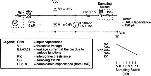
The signal source, together with internal resistance, is depicted to the left of the diagram, modelled as voltage source in series with internal resistance. The signal voltage enters the microcontroller through the pin labelled ANx. There is a small input capacitance (5 pF), and the input protection diodes and other input circuitry clearly have the potential to leak current into the signal path. The signal then passes through the interconnect resistance, RIC, before reaching the multiplexer switch. This is one of the switches of the analog input multiplexer in Figure 11.6. The internal resistance of this switch, RSS, is shown. The approximate value of this is dependent on supply voltage and is given by the small graph on the bottom right of Figure 11.10. From this we see that the switch resistance is a sobering 7 kΩ approximately, when the supply voltage is 5 V.
The ADC itself is a so-called switched capacitor type (Ref. 1.1, Chapter 5). First of all, that means that the ADC has internal capacitance, which must be charged up to the input voltage before a conversion can start. Neatly, however, this capacitance takes on the function of the S&H capacitor. On the downside, the capacitance, all 120 pF of it, must be charged up in the first place.
11.3.4 Calculating acquisition time
In Ref. 7.1 Microchip define three sources of time delay in their calculations for acquisition time, tac, as shown:
The reference specifies the amplifier settling time as a fixed 2 μs. The temperature coefficient applies only when temperature is above 25°C and is specified as:
It can be seen that this creates a time delay of only 0.5 μs for every 10° above 25°, so its impact in most cases is slight.
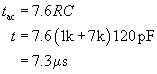
It is the capacitor charging time that dominates the acquisition time, which we now explore. The analog input model of Figure 11.10 can be related back to the S&H diagram of Figure 11.3 and Equation (11.1). To analyse this, we neglect the effects of the input leakage current and the small input capacitance. Actual values for R and C in Figure 11.3 for the 16F87XA ADC can be extracted from Figure 11.10. R is made up of (RSS + RIC + RS), or (1k + 7k + RS), for a supply voltage of 5 V. C is the 120 pF shown. Calculations made for Figure 11.4 showed us that, for 10-bit accuracy, an acquisition time of 7.6RC was needed. Substituting values in, assuming at first negligible source resistance, gives:
If amplifier settling time is added to this, as it must be, the acquisition time rises to 9.3 μs.
This represents a best possible value. To determine the overall time needed to complete a single conversion, this acquisition time must be added to the conversion time, discussed in Section 11.3.2. There, a best possible conversion time of 19.2 μs was deduced. Adding this to the best possible acquisition time leads to a total time to complete a conversion of (2 + 7.3 + 19.2) μs, i.e. 28.5 μs.
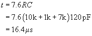
In many cases the source resistance is not negligible and any external series resistance will degrade the acquisition time calculated above. In Ref. 7.1 Microchip recommend a maximum source resistance of 2.5 kΩ. In this case:

Note that this is not the highest acquisition time that may be encountered, as the maximum allowed source resistance is specified in Ref. 7.1 as being 10 kΩ.
11.3.5 Repeated conversions
When a conversion is complete, the converter waits for a period of 2 × TAD before it is available to start a new conversion cycle. Once this time is up, either the same input channel may be converted again, or a new one (which may already have been selected) may be converted.
A best possible conversion time of 28.5 μs was calculated in Section 11.3.4. If a period of 2 × TAD is added to this, i.e. 3.2 μs for fastest possible, then the complete conversion cycle time becomes 31.7 μs. If successive conversions are intended, this implies a maximum sampling rate of around 30 kHz. Note, however, that this figure takes no account of software overheads, which would tend to slow the conversion rate.
11.3.6 Trading off conversion speed and resolution
The conversion times deduced above are not particularly fast by today's standards and there will be occasions when a faster conversion time is needed. While one option is to use an external ADC, another is to consider whether the full 10-bit resolution is needed. If it is not, then the conversion time can be reduced. One technique, described in Ref. 11.1, is to start a conversion with a valid ADC clock frequency and then to switch it during the conversion to a faster speed, which violates the clock specification. The higher-order bits converted before the switch will be valid and can be used. Those converted after will not be valid. A lower-resolution conversion, at higher speed, has thus been achieved. It is up to the programmer, however, to determine when the switch should take place.
An alternative approach is to reduce the acquisition time, as suggested in Figure 11.4, so that, for example, the acquisition is only to 8-bit accuracy. The conversion can then be allowed to run its full course. The switching of the ADC clock frequency, as just described, can still be implemented.
11.4 Applying the analog-to-digital converter in the Derbot light meter program
The Derbot AGV has three light-dependent resistors, used as light sensors, as seen in Figure A3.1. Two are at the front and one at the rear of the vehicle. The Derbot uses the 16F873A ADC to measure light intensity, for both a light meter program and a light-seeking program.
Program Example 11.1 shows sections of the program Dbt_light_meter, reproduced in full on the book's companion website. The program reads the LDR output values and displays these on the LCD of the hand controller unit. There are, however, several data manipulation challenges on the way. The result of the ADC must be scaled to a true voltage reading and then converted to a format suitable for the LCD. Therefore, the reading is converted to Binary Coded Decimal and then to ASCII. The resulting characters are then transferred to the LCD. Let us explore how this is done.
11.4.1 Configuration of the analog-to-digital converter
The initial setting of the ADC control registers, ADCON0 and ADCON1, can be seen in the program example. Figure A3.1 shows that the right LDR is connected to Port A bit 0, the left to Port A bit 1 and the rear to Port A bit 3. No external reference voltage is available, so the power supply is used. These connections lead to the PCFG bits in ADCON1 (Figure 11.8) being set to 0100.
With a main clock period of 250 ns (4 MHz), but a minimum specified Tad time of 1.6 μs, it is necessary to divide the clock frequency by at least eight. This value is chosen, giving a Tad of 2 μs. A right-justified result is selected.
11.4.2 Acquisition time
The operation of the data acquisition can be examined by looking further down the program example.
The acquisition time needs to be calculated for the worst-case condition, which is when ambient light is low and the LDR resistance high. This may be checked in the LDR data [Ref. 8.5]. In the worst case the LDR resistance will be very high and the source resistance will tend towards the value of the 10 kΩ resistor in series with the LDR. Note that this is at the limit of the maximum allowed source resistance. However, under normal lighting conditions the source resistance will be considerably lower. From Figure 11.4, acquisition time is given by:
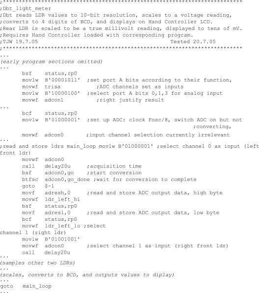
11.4.3 Data conversion
The actual operation of the ADC can be seen by checking further down the program example, from the label main_loop. The three LDRs are sampled in turn. For the first (front left), it can be seen that the appropriate input channel is selected, with the GO/DONE bit of ADCON0 left low. A delay of 20 μs is introduced for signal acquisition, which just covers the calculated worst-case value of 18.4 μs. The actual conversion is then initialised by setting the ![]() bit high. Completion of conversion is awaited by testing the same bit. The result of the conversion is then transferred from ADRESH and ADRESL to the two stores in memory, and the program moves on to sample the next input. The data manipulation that follows is omitted in this program example, but is described later in the chapter.
bit high. Completion of conversion is awaited by testing the same bit. The result of the conversion is then transferred from ADRESH and ADRESL to the two stores in memory, and the program moves on to sample the next input. The data manipulation that follows is omitted in this program example, but is described later in the chapter.
11.5 Some simple data manipulation techniques
Almost as soon as data is acquired in a program there follows the need to manipulate it in some way. This could include simple addition and subtraction, as we have already done, or other arithmetic operations like multiplication and division. As the data processing demand rises, so most certainly does the Assembler complexity, creating a strong motivation for a move to a high-level programming language. Nevertheless, it should not be necessary to write a program or subroutine for any standard mathematical operation in Assembler. Many are already available, for example in Ref. 11.2.
11.5.1 Fixed- and floating-point arithmetic
We have already repeatedly used the fact that an n-bit binary number can represent any integer number value from 0 to 2n – 1. For example, an 8-bit number can represent from 0 to 255D, a 12-bit number from 0 to 4095D, and a 16-bit number from 0 to 65 535D. For larger numbers, more bits just need to be added. We could even represent fractional numbers in this way, by inserting a binary point. Then the digits to the right of the binary point represent negative powers of two. This is seen in the example of Figure 11.11, where the binary number 1101.11 is evaluated to 13.75D. As long as the binary point remains in the same fixed place in all numbers being used (in fact, we only need to imagine it there), then it is possible to undertake a range of arithmetic operations with a set of numbers.

This type of binary number representation is called ‘fixed point’. The binary point is not used, or else is assumed to be in a fixed place in the number. Such representation can solve the need to represent integers and non-integer numbers. It does not, however, solve the problem of dealing with number values that range from the very small to the very large. The smallest non-zero number that the 6-bit fixed-point number of Figure 11.11 can represent, for example, is 0.25D, while the maximum number is 15.75D. It could neither represent 0.0004D nor 2.3 × 10⁶.
The solution to this problem lies in ‘floating-point’ representation. This represents the number with a ‘sign bit’, ‘mantissa’ and ‘exponent’. A huge range of numbers can be represented, but processing complexity is greater. While floating-point routines are available in Assembler, they are most commonly found in high-level languages, where they are used for all precision calculation. In this chapter we apply only fixed-point arithmetic.
11.5.2 Binary to Binary Coded Decimal conversion
While all fixed-point arithmetic is done in binary, where there is human interaction, there will be a marked preference for decimal. How do we move data between the binary domain and the decimal?
A simple halfway house between binary and decimal is Binary Coded Decimal (BCD). This uses a 4-bit number to represent a decimal digit, as shown in Table 11.2. The only thing that distinguishes BCD from hexadecimal is that in BCD the binary equivalents of hex. AH, BH, CH, DH, EH or FH are not allowed. Thus, Table 11.2 shows all legal BCD codes for a single decimal digit. The table also shows the ASCII (American Standard Code for Information Interchange) code for each of the numbers. For numeric characters, it can be seen that this is simply a single-byte code in which the number itself occupies the lower nibble and the number 3 forms the higher.
TABLE 11.2 Binary, Binary Coded Decimal and American Standard Code for Information Interchange
| Decimal | Binary (BCD) | ASCII (in hex.) | Decimal | Binary (BCD) | ASCII (in hex.) |
|---|---|---|---|---|---|
| 0 | 0000 | 30 | 5 | 0101 | 35 |
| 1 | 0001 | 31 | 6 | 0110 | 36 |
| 2 | 0010 | 32 | 7 | 0111 | 37 |
| 3 | 0011 | 33 | 8 | 1000 | 38 |
| 4 | 0100 | 34 | 9 | 1001 | 39 |
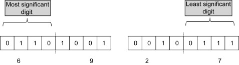
Given this simple coding, multi-digit decimal numbers can be represented in BCD. In ‘packed BCD’, which is commonly used, a byte is used to represent two decimal digits. An example is shown in Figure 11.12.
Despite this simple representation, it is not completely straightforward to convert between BCD and binary. Standard algorithms are available, however, such as are used in Ref. 11.3. The Derbot light meter example uses a subroutine taken from this reference that converts a 16-bit number into a five-digit BCD number. This is used to prepare the data for the display. The underlying algorithm can be found in many books on computer arithmetic and in Ref. 1.1.
11.5.3 Multiplication
After addition and subtraction, multiplication is the next most common arithmetic requirement that is usually needed in computer arithmetic. Some processors have hardware multipliers in them and hence a multiply instruction. For the simpler ones, like the PIC 16 Series, multiplication must be achieved by software routines. The standard algorithm for this is a repeated shift and add process [Ref. 1.1]. A very wide range of standard routines are available, in both fixed point and floating point. The fixed-point ones come in different sizes, depending on the number size to be used. Inevitably, those with longer word length take more time to execute. Reference 11.2 has fixed-point multiply routines for 8-bit × 8-bit (with 16-bit result), 8-bit × 16-bit (with 24-bit result), and 16-bit × 16-bit up to 32-bit × 32-bit (with 64-bit result).
The Derbot light meter example uses a 16-bit × 16-bit multiply subroutine taken from Ref. 11.3, as is now described.
11.5.4 Scaling and the Derbot light meter example
A common application of multiplication is for scaling of input data, perhaps to convert it into a standard unit. The Derbot example is interesting in this respect.
The Derbot uses the power supply voltage of 5 V as its reference. Hence the 10-bit resolution is (5/1024) = 4.883 mV. Thus, the ADC least significant bit, when using this voltage reference, is ‘worth’ 4.883 mV. If the ADC output value is multiplied by 4.883, then the result will give a true millivolt reading. Yet it is awkward to introduce and track a binary point. A possible workaround is to scale the fractional number up by a binary power and then – after the multiplication – divide by the same number. It's easy to do this, as binary division is a straightforward process of shifting a number right, effectively discarding less significant bits.
For example, for the Derbot light meter, we want to do the calculation:
While we can't multiply by 4.883, we note that 4.883 × 256 = 1250.048 and we can do the following multiplication using integers only:
With the ADC output being a 10-bit number and 1250D (i.e. 04E2H) an 11-bit number, the result will be at most 21 bits. This defines the type of multiply routine needed.
If the intermediate result is then divided by 256, which can be done simply by discarding its least significant byte, then our scaling process is complete. The outcome is the voltage input to the ADC, given in millivolts.
One is justified in asking how the multiplying factor of 256 was chosen, rather than say 128 or 512. This depends on the rounding or truncation error introduced. The error in taking 1250 instead of 1250.048 is very small, well below 0.05 per cent, and so is acceptable when dealing with 10-bit numbers. In fact, it would have been acceptable to use 128 as the multiplying factor, but then the convenience of dropping the least significant byte for the division stage would have been lost.
Remember that all of this is a workaround. We could alternatively convert 4.883 directly to binary, which turns out to be 100.11100010, or 4.E2H. With a bit of thought, and comparing this number with the multiplier we found above, it can be seen that the two methods are essentially equivalent.
The process described above is applied in Program Example 11.2, which scales the value of the rear LDR. It uses two subroutines: mult16x16 to multiply two 16-bit numbers and Bin2BCD16 to convert a 16-bit number to a five-digit BCD output. The program section starts after the ADC conversions have been made. The stored output of the ADC conversion, held in memory locations ldr_rear_hi and ldr_rear_lo, is transferred into aargb0 and aargb1, one of the 16-bit inputs to the multiplier subroutine. The other input to the subroutine is the word formed by bargb0 and bargb1. Into this is loaded the word 04E2H, the hexadecimal equivalent of 1250D. The mult16x16 subroutine is then called, with the result being placed in aargb0:aargb1:aargb2:aargb3. As the result can only be 21-bit, the most significant byte aargb0 will be empty and is ignored. The least significant byte is similarly ignored, as the result needs to be divided by 256. The next byte up, aargb2, is the less significant byte of the required result and is therefore transferred into the lower byte (templ) of the 16-bit input to the Bin2BCD16 subroutine. Similarly, aargb1 is transferred to the upper byte, temph. The Bin2BCD16 subroutine is then called. The output bytes of this are immediately used for transfer to the LCD, by the subroutine four_dig_disp. This sends the BCD characters in turn on the I2C link, for display on the hand controller LCD.
Program Example 11.2 Data processing sequence for rear light-dependent resistor, Derbot light meter program

All subroutines appear in the complete program listing on the book's companion website.
11.5.5 Using the voltage reference for scaling
The fact that the ADC output in the Derbot example immediately needs to be scaled, in order to provide a true voltage reading, can be annoying, and of course use of the multiply routine itself is time-consuming in program execution.
In some cases a judicious choice of voltage reference value can significantly simplify further calculations that need to be made. For example, if the Derbot ADC was fitted with a reference of 4.096 V, then 1 LSB of the output would represent 4 mV exactly and complex scaling would not be needed. Similarly, if the reference voltage was 1.024 V, then 1 LSB of the output would represent exactly 1 mV. Voltage references with values such as these are readily available for this very purpose.
11.6 The Derbot light-seeking program
This program gives another example of use of the 16F873A ADC. By comparing measurements between the three LDRs, the AGV finds the source of brightest light and moves towards it. It moves at a speed dependent on the light difference between its sensors, so comes to a halt when all three are at similar levels of illumination. As only comparative measurements are being made, the application does not require high accuracy. Therefore, only an 8-bit ADC result is used in the program. It is therefore more convenient to left-format the result (Figure 11.9), so that the result can be taken from just the eight bits of register ADRESH. This can be seen in the changed setting for ADCON1 in this example.
With only an 8-bit result in use, the opportunity presents itself to shorten the acquisition time, notionally to 6.2RC (Figure 11.4). As the program will only operate in reasonable levels of ambient light, the highest LDR resistance is estimated to be 10 kΩ, giving a revised maximum source resistance of 5 kΩ. The ADC input capacitance remains at 120 pF, as do the internal series resistances of the ADC. The acquisition time is therefore 6.2 × 13 k ×120 pF, or 9.7 μs. An 11 μs delay subroutine is used.

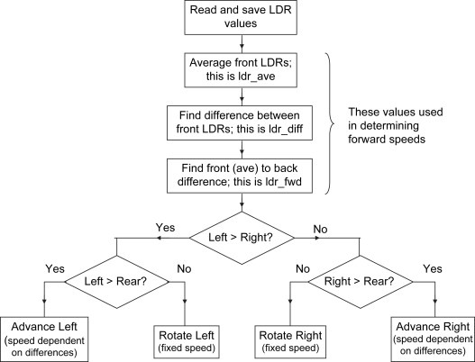
The actual control algorithm is represented in Figure 11.13 and is repeated approximately every 200 ms. The full listing can be found on the book's companion website. Having read each LDR value, it makes some preliminary calculations of average and difference values, used later if a forward speed is to be calculated. It then determines the brightest LDR and takes appropriate action. If front left or front right are brightest, it moves forward, turning in the brighter direction, with a speed and turn dependent on the relative light intensities. If the rear is brightest, however, it rotates on the spot for a fixed period, in the direction of the front LDR that is brighter.
To configure the Derbot as a light-seeking AGV, the LDRs and their resistors should be added to the board. Download the Dbt_light_seek project from the book's companion website and create an MPLAB project around it. Adjust the program initialisation to match your build, setting all unused port bits to output. Build the program and download to the microcontroller. The Derbot should be immediately ready to run in light-seeking mode. This works well in a space where there is a clear variation of light. The Derbot will struggle in a space where the light is mottled or patchy, and will sit completely still in a space that is uniformly lit!
11.7 The comparator module
Having explored the intricacies of the ADC, we end the chapter with one of the simplest interfaces between the analog and digital world – the comparator. This important circuit element acts a little like a 1-bit ADC. It is usually used to compare an input voltage with a reference. If the input is higher than the reference, the comparator output goes high; if it is lower, the output goes low. There are many applications for comparators in embedded systems. These include cleaning up corrupted digital signals (in which case their use is very close to a Schmitt trigger), testing battery voltage, setting an alarm if a temperature or other variable reaches a certain value and so on.
11.7.1 Review of comparator action
A comparator is shown in Figure 11.14(a). The comparator simply compares its two inputs, shown in the diagram as V+ and V–. If V+ is greater than V–, then the comparator output goes to a positive voltage value, usually the maximum ‘saturated’ voltage level. If V+ is less than V–, then the output goes to a negative or zero voltage value. With suitable design of output circuit, the output voltage levels can easily be made to be recognisable logic levels.

An example of input and output voltages is shown in Figure 11.14(b). V− has been set to a fixed voltage, shown by the dotted line, while V+ is varying. Whenever V+ is greater than V–, the output goes to Logic 1; when it is less, the output goes to Logic 0.
11.7.2 The 16F87XA comparators and voltage reference
The 16F87XA has two comparators, which share inputs with the ADC inputs. Comparator 1 has inputs on AN0 and AN3, and comparator 2 on AN1 and AN2. They are controlled by the CMCON register, seen at address 9CH in Figure 7.6. A number of different configurations are possible. For example, comparator outputs can be routed externally, to pins RA4 and RA5, or they can simply appear as bits in the CMCON register. These can be easily looked up in the Microchip data [Ref. 7.1] and are not enumerated here. Importantly, the comparators also form an interrupt source. A change in state of either comparator will set the CMIF flag, seen in Figure 7.10.
The 16F873A also has a voltage reference module, under the control of the CVRCON register (address 9DH). This is a resistor ladder, connected at one end to the supply voltage (via a switching transistor), which allows different voltage values to be selected as the reference. The voltage reference can be used as an input to one or both comparators, and can be output through pin 4 of the 16F873A. In this case, it can be used as a very crude ADC output.
11.8 Applying the Derbot circuit for measurement purposes
We have now reached a stage where we can acquire input analog voltages, process the data acquired and then display it. This is a very powerful position, as it is the basis of many a measurement system. This section describes how the Derbot PCB and hand controller can be used to create certain measurement tools, using programs already described. The hand controller connects to the Derbot ‘bus’ connector, which lies physically at the lower end of the microcontroller IC holder. It should be loaded with its standard program, i.e. that of Program Example 10.3.
These projects can be created as stand-alone devices or incorporated into the AGV. If stand-alone, then of course the end product is a little bulkier than one would wish. The option remains to redesign the hardware to create a more compact outcome. The circuit required, if stand-alone projects are being made, is shown in Figure 11.15. This shows the components and connections needed for all three items. The sections below will indicate which ones are needed for any single build.
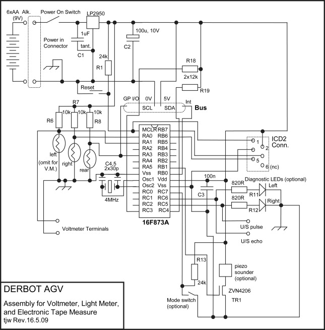
When programming, ensure as always that all unused port bits are set as outputs. Check, therefore, your build against the program initialisation in use and adjust if necessary.
11.8.1 The electronic tape measure
The ultrasound test program, shown in part in Program Example 9.7, forms the basis of an ultrasonic ‘tape measure’, displaying in centimeters the distance from the sensor to a reflecting surface. It processes data in a similar way to the light meter program of Program Example 11.1 and therefore shares a number of features with it.
To build the tape measure as a stand-alone unit, the circuit of Figure 11.15 needs to be built on the Derbot PCB, but without the LDRs and their resistors. A Devantech SRF04 or SRF05 ultrasonic sensor should be used. A set of connection points for this is available just forward of the motor locations on the Derbot PCB. Terminal pins should be soldered in here, or a PCB-mounting screw-terminal block used. Applying the sensor data [Ref. 8.7], connect 0 V, 5 V, pulse and echo to the pins, and glue or attach the sensor to a place of your choosing on the PCB. A completed unit is shown in Figure 11.16. Power is supplied from a 9 V PP3 battery held between main and hand controller boards. It connects with a flying lead to the main power input.
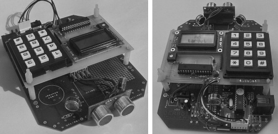
Complete the build as described and create an MPLAB project around the Dbt_US_Test program, shown in part in Program Example 9.7. Adjust the initialisation to match your build, setting all unused port bits to output. Build the program and download to the microcontroller. Point the sensor at a reflective surface, and the distance between sensor and surface should be continuously displayed in centimetres on the hand controller display.
11.8.2 The light meter
To create the light meter, build the circuit of Figure 11.15 without the ultrasonic sensor. Download the Dbt_light_meter project from the book's companion website and create an MPLAB project around it. Adjust the program initialisation to match your build, setting all unused port bits to output. Build the program and download to the microcontroller. Run the program and see how all LDR readings are displayed. As discussed, each reading is in millivolts, but gives an indication of light intensity. Notice that the reading goes down as the light intensity increases.
11.8.3 The voltmeter
It is a simple matter to adapt the light meter program to a voltmeter. In this case, the LDRs should not be built onto the board. The voltmeter input is shown connected across the left LDR, although any other LDR connection points can be chosen. Input terminals for the voltmeter can be placed in the prototype area and connected appropriately.
Download the Dbt_light_meter project from the book's companion website and create an MPLAB project around it, giving it a name appropriate to this project. Adjust the program initialisation to match your build, setting all unused port bits to output (and noting that two ADC inputs are now no longer used). The program can otherwise be used as it is. It is better, however, to remove the two unused ADC readings and the two redundant displayed values, which will now have no meaning, unless a multi-input voltmeter is wanted. To test, connect a variable DC voltage input to your voltmeter input and connect a digital voltmeter across this. Check whether the two voltmeter readings agree.
This adaptation of the Derbot core design leads to a fairly inaccurate voltmeter, as the voltage reference is the power supply. The place of the rear LDR can, however, be taken by a voltage reference of appropriate value. It can be seen from Figures 11.6 or 11.8 that this input can be reconfigured as a reference input. The software scaling will need to change to reflect any change in reference value. By making these changes, a voltmeter of reasonable accuracy can be developed.
11.8.4 Other measurement systems
It is very easy to adapt the ideas already applied here to other measurement systems. This applies to any sensor that has a voltage output. There is, for example, a range of semiconductor temperature sensors that have a voltage output directly dependent on temperature. One of these could be used, either on a flying lead or soldered into the prototyping area. With the scaling adjusted, a digital thermometer can readily be developed.
Summary
• Most signals produced by transducers are analog in nature, while all processing done by a microcontroller is digital.
• Analog signals can be converted to digital form using an analog-to-digital converter (ADC). The ADC generally forms just one part of a larger ‘data acquisition system’. ADCs represent a fascinating interface between the analog and digital worlds.
• Considerable care needs to be taken in applying ADCs and data acquisition systems, using knowledge of among other things timing requirements, signal conditioning, grounding and the use of voltage references.
• The 16F873A has a 10-bit ADC module that contains the features of a data acquisition system. An understanding of such systems is essential in applying this module.
• Data values, once acquired, are likely to need further processing, including offsetting, scaling and code conversion. Standard algorithms exist for all of these, and Assembler libraries are published.
• A simple interface between the analog and digital world is the comparator, which is commonly used to classify an analog signal into one of two states.
11.1. PICmicro Mid-Range MCU Family Reference Manual (1997). Microchip Technology Inc., Section 23, DS31023A.
11.2. Fixed Point Routines (1996). Microchip Technology Inc., Application Note 671, Document no. DS00617B.
11.3. Watt-Hour Meter using PIC16C923 and CS5460 (2000). Microchip Technology Inc., Application Note 671, Document no. DS00220A.
Questions and exercises
1. A Sample and Hold circuit, of the form shown in Figure 11.3, is connected to a signal of source resistance 2 kΩ; its output is connected in turn to an ADC. The Sample and Hold capacitor is 90 pF.
2. A 16F873A microcontroller is supplied with 5 V. Its ADC is connected so that the voltage reference is taken from its supply voltage and ground.
3. In a certain application all available channels of a 16F873A ADC are used for analog input, except that an external voltage reference is required. The 0 V side of this is connected to system earth. The internal ADC oscillator is to be used as the clock source, and the result is to be right-justified.
4. A 16F873A microcontroller is operating from a supply of 4 V and a clock frequency of 1 MHz. The ADC is used, but only 8-bit accuracy is required. The signal source resistance is 5 kΩ.
5. A temperature sensor is connected to a 16F873A ADC input. The sensor has an output of 40 mV/°C. The ADC operates with a 4.096 V reference.
(a) For a certain temperature value, the ADC output reads 1010011100. What is the equivalent temperature for this reading?
(b) The measured temperature is to be displayed on a digital display, showing values in the range 00.0°C to 99.9°C. Describe what data manipulation steps can be taken to achieve this, using fixed-point arithmetic only.