
Linear Doherty Power Amplifier for Handset Application
Abstract
Doherty power amplifier is a good solution for amplification of a high PAPR signal as clearly seen from the popularity in the base-station amplification. But the amplifier is less popular for handset application because of the nonlinear behavior and complex circuit topology. However, those problems can be solved by elaborated circuit design works. The bulky input power divider and quarter-wavelength transmission line can be replaced by simple circuits with small sizes. Therefore, the Doherty structure could be integrated into a single chip with a small size. The linear Doherty power amplifier is realized by the harmonic cancellation between the carrier and peaking amplifiers. This chapter is devoted to these linear Doherty amplifier design techniques for handset applications. The design technique using GaAs HBT is described in detail, and CMOS Doherty power amplifier is also discussed.
Keywords
Linearity; Harmonic cancellation; Compact design; Input divider; CMOS Doherty amplifier; Average power tracking (APT); Gain modulation
Doherty power amplifier is a good solution for amplification of a high PAPR signal as clearly seen from the popularity in the base-station amplification. But the amplifier is less popular for handset application because of the narrow bandwidth and complex circuit topology. However, those problems can be solved using elaborated circuit design works. This chapter is devoted to the Doherty amplifier for handset application. The design technique using GaAs HBT will be described in detail, and CMOS Doherty power amplifier will also be discussed.
5.1 Introduction
For the mobile handset application, the Doherty structure should be integrated into a single chip with a small size. The bulky input power divider and quarter-wavelength transmission line must be replaced by circuits with small sizes. Above all, the linearity of the handset Doherty power amplifier should be considered more carefully than that of the base-station amplifier because the powerful digital predistortion technique is not usually employed.
The ideal Doherty amplifier is linear because the uneven powers from the carrier- and peaking amplifiers are combined perfectly, providing the linear AM-AM characteristic as discussed in Section 1.2.2. But the real transistor responses are different from the ideal class B and C bias operations, and the nonlinear responses should be corrected to get the linear response. The class B carrier amplifier should be replaced by a linear class AB amplifier because only the carrier amplifier is operated at the low-power region. The nonlinear operation of the class C peaking amplifier should be linearized. The natural choice for linearization of the Doherty power amplifier is to compensate the gain compression of the class AB carrier amplifier and the gain expansion of the class C peaking amplifier. For the purpose, the peaking amplifier should be turned on early, and the third-order intermodulations (IM3) of the two amplifiers should be adjusted properly for the IM3 cancellation. The even harmonics should be suppressed by the harmonic short load since the harmonics can generates the noncancelable IM3 component through the interaction with the fundamental component. Also, the uneven drive is necessary to get the ideal Doherty amplifier operation.
In this chapter, detailed design processes of a linear Doherty power amplifier for handset will be introduced. For a compact design, the quarter-wavelength inverter is replaced by a proper lumped quarter-wave transformer, and a bulky input power divider is replaced by a direct input-power-dividing circuit. The direct dividing circuit can optimize the load modulation characteristic through the proper uneven input drive and reduces the number of the circuit components. The gain modulation properties of the carrier and peaking amplifiers are analyzed, and a method to get a linear AM-AM characteristic is introduced. A proper lumped quarter-wave transformer and harmonic terminations are introduced to improve the linearity. Based on the concept, a linear Doherty power amplifier is designed using heterojunction bipolar transistor (HBT), since HBT is the most favored technology for handset power amplifiers.
The same technique can be applied to a CMOS Doherty power amplifier. In the CMOS power amplifier, the output power is voltage-combined using a transformer. The operation behavior of the CMOS Doherty amplifier based on the transformer is described in Section 1.4.1.
5.2 Design of Linear Doherty Power Amplifier
5.2.1 Load Modulation of Doherty Amplifier Based on HBT
In the Doherty amplifier at a low power operation, the input power is divided by a 3 dB coupler, and the 3 dB lower input power is delivered to the carrier, producing a 3 dB loss. Therefore, the overall gain of Doherty amplifier is equivalent to the gain with ROPT load. At the peak power operation, the carrier and peaking amplifiers become a two-way current power combining structure with ROPT load, and the gain is the same as at a low-power level. In between the two power levels, due to the nice asymmetrical power combining, the gain is maintained as we have described in Section 1.2.2. Due to the constant gain characteristic, the Doherty amplifier is a linear amplifier. However, in the practical design of the Doherty power amplifier using an HBT, the ideal gain characteristic is not produced.
5.2.1.1 Gain Modulation of Carrier Amplifier
Fig. 5.1 shows the nonlinear equivalent circuit model of an HBT. In the HBT model, Cbe, gbe, and gm are strong nonlinear components, varying as an exponential function of Vbe. But their responses are canceled out since the output current gmVbe is proportional to gm/(jωCbe + gbe). And the main nonlinear component of an HBT is Cbc.

Cbc is the base-collector depletion layer capacitance, and it is decreased with Vbc because of the increased depletion size. The injected collector current also reduces the capacitance since the injected electron neutralizes the collector depletion donor and extends the depletion layer size. The capacitance variation is shown in Fig. 5.2. Since the current level is larger for the ROPT operation than the 2ROPT operation, the feedback capacitance Cbc is larger for 2ROPT operation with similar Vbc swing. Therefore, the gain at 2ROPT is reduced significantly by the strong feedback capacitance Cbc.

Fig. 5.3 shows the simulation results of the power gains for various output loads using the real device model. As shown in the figure, the power gains for both cases with the ROPT and 2ROPT are almost the same value regardless of the HBT size. The gain characteristic of the carrier amplifier makes it difficult to get a good AM-AM characteristic from the Doherty amplifier, but still linear Doherty amplifier operation is possible.

5.2.1.2 Flat Gain Operation of Doherty Amplifier Based on HBT
Under the ideal condition, the carrier amplifier operation with 2ROPT load, at a low power region, has 3 dB higher power gain than the amplifier operation with the ROPT, but there is 3 dB input power loss, compensating the gain. At the higher power operation, the gain reduction of the carrier amplifier with the ROPT load is compensated by the peaking amplifier. Therefore, the constant gain is maintained. However, in real device implementation, the gain reduction cannot be compensated by the peaking amplifier because it requires the gm of the peaking amplifier two times larger than that of the carrier amplifier as described in Section 1.2. It means that the peaking transistor should be two times larger than that of the carrier amplifier, wasting the power generation capability of the peaking amplifier. Moreover, the gain of the peaking amplifier is a lot lower than that of the carrier amplifier due to the class C bias. Therefore, the total gain of the Doherty power amplifier is distorted as shown in Fig. 5.4 (Gain_ideal case). This distortion can be compensated somewhat by the uneven driving as discussed in Section 2.1.

In the real device operation, the gains of the carrier amplifier with the ROPT and 2ROPT loads are almost the same value. Therefore, to get the proper Doherty load modulation characteristic, the carrier amplifier should be saturated in the modulation region with about 3 dB gain compression at the maximum output power by driving the carrier amplifier with a higher power. Due to the lower saturated gain of the carrier amplifier, the peaking amplifier can compensate the low gain, assisting for the proper Doherty operation with a constant gain as shown in Fig. 5.4. In the low-power region, only the carrier amplifier operates and should be linear. Therefore, the carrier amplifier should be designed as a linear amplifier at 2ROPT load with a class AB bias. At the higher-power region, the IM3 components generated by the carrier amplifier and peaking amplifier should be canceled.
5.2.2 IMD3 Cancellation With Proper Harmonic Load Conditions
At the load modulation region with the quasisaturated operation of the carrier amplifier, the cancellation of the third-order intermodulation distortions (IMD3s) generated by the carrier and peaking amplifiers is the most important design issue in realizing a linear Doherty power amplifier. In a simple power series expression of the gain using a two-tone signal, the fundamental output power is expressed as

The output of the third-order intermodulation (IM3) is given by

Here, a1 is the linear gain coefficient, and the other terms ai represent the higher-order harmonic generation coefficients as described in Section 4.1.3. In Eq. (5.1), the linear gain is distorted by the higher-order harmonic generation.
The gain expansion occurs for a class C biased amplifier since a3/a1 and a5/a1 are positive. Therefore, the IM3 and fundamental signals of the peaking amplifier are in-phase. On the other hand, the gain compression occurs in the class AB biased carrier amplifier with negative a3/a1 and a5/a1, and the IM3 and fundamental signals are in antiphase. By using the complementary gain characteristics of the carrier and peaking amplifiers, the IMD3s of the two amplifiers can cancel each other, thereby improving the linearity of the Doherty power amplifier. These coefficients are strongly bias-dependent, and the gate biases of the carrier and peaking amplifiers should be properly adjusted for the cancellation.
In Eq. (5.2), the IMD3s at the lower and higher frequencies of the two-tone signal are the same magnitude, and the symmetrical IMD3 can be canceled. However, the different phased IM3s having different magnitudes are produced by the interactions of the fundamental and the feedback even-order intermodulation harmonic terms. This nondirectly generated IM3 terms, not included in the power series equations, cannot be canceled, deteriorating the IMD3 cancellation. The IM2, which is the most important even harmonic, should be suppressed by a second-harmonic termination, thereby alleviating the IM3 generation.
Fig. 5.5 shows the ideal simulation of the IM2 generation according to the conduction angle. As shown, the class AB and C amplifiers generate significant IM2s with different magnitudes according to the conduction angle. To investigate the harmonic suppression behavior, a two-tone simulation is conducted. In this simulation, an ideal second-harmonic short termination shown in Fig. 5.6 is attached under the condition that it doesn't affect the fundamental and other harmonic loads. The second-harmonic short at the output of peaking amplifier provides the same short condition at the output of the carrier amplifier because the quarter-wave line at a fundamental frequency turns into a half-wave line at the second-harmonic frequency.


Fig. 5.7A shows the magnitude and phase differences between the IM3s of the carrier and peaking amplifiers, IC.IM3 and IP.IM3. With the second-harmonic short, IC.IM3 and IP.IM3 are in near antiphase condition because the additional components produced by the even-order harmonics are suppressed. Also, the magnitude difference is in near zero. Therefore, the Doherty power amplifier with the second-harmonic short has a lower IMD3, through the IM3 cancellation, than the other case as shown in Fig. 5.7B. Moreover, the power amplifier with the second-harmonic short delivers a higher power-added efficiency (PAE) because it produces a class F waveform. The second-harmonic short circuit generates a half-sinusoidal shaped current waveform with the in-phase second-harmonic current, and the high third-harmonic load is easily produced internally for a rectangular-shaped voltage waveform.

The efficiency and linearity at the 6 dB power back-off (PBO) region are closely related to the turn-on timing of the peaking amplifier. Since the peaking amplifier cannot be abruptly turned on, it should be turned on early to compensate the AM-AM and AM-PM distortions of the carrier amplifier for achieving high linearity at the 6 dB PBO, but the early turn-on means that the load modulation starts early, before the carrier reaches to the saturated operation, and the efficiency at the 6 dB PBO is reduced.
Fig. 5.8 shows the effect of the turn-on timing of the peaking amplifier. The lower bias of the peaking amplifier boosts the efficiency of the 6 dB PBO, but the peak efficiency is decreased since the output power of the peaking amplifier is reduced due to the deeper class C bias. Moreover, the AM-AM and AM-PM are deteriorated leading to a poor linearity. For a linear Doherty power amplifier, therefore, the base bias of the peaking amplifier should be chosen properly to make the linear AM-AM and AM-PM responses.

5.3 Compact Design for Handset Application
Compact design of the Doherty amplifier is essential for handset applications. Fig. 5.9A shows a conventional Doherty structure, which uses a power divider such as a coupler for the inputs of the both amplifiers, a quarter-wavelength line for load modulation, and offset lines for imaginary impedance modulation. The functional blocks can be simplified by merging the functional circuit components as shown in Fig. 5.9B. The offset lines are eliminated by terminating the output capacitance at the drain terminal before the output matching circuit, thereby eliminating the imaginary part impedance transformation by the matching circuit. The input power divider can be eliminated by the direct power-dividing approach. However, the coupler-based power divider provides a lot of stable operation with accurate power-dividing ratio, and it is a design option between the compact size and the stable operation.

5.3.1 Input Power Dividing Circuit
Fig. 5.10 shows the two input-power-dividing circuits: coupler divider and direct power divider. For mobile applications, a bulky input power divider can be removed by a direct input-power-dividing technique shown in Fig. 5.10B. For the ideal input power driving, the carrier amplifier should receive more power in the low-input-power region when the peaking amplifier is turned off, compensating the low gain at 2ROPT operation, and the peaking amplifier gets more power in the high-input-power region to increase the gain and output power of the class C biased peaking amplifier.
The uneven power dividing can be realized using the power-level-dependent input impedance variations of the carrier and peaking amplifiers. The input capacitance Cin of an HBT shown in Fig. 5.1 is determined by Cbe and miller capacitance Cbc. The capacitance is expressed as.
where RL is the output load impedance. Fig. 5.11 shows the Cin variations for the carrier and peaking amplifiers.

Because of the class C bias of the peaking amplifier, the large-signal transconductance (gm) and Cbe of the peaking amplifier vary significantly, while those of the carrier amplifier remain almost constant. The input capacitance of the peaking amplifier increases over 200% as the input power increases, while that of the carrier amplifier varies less than 10%. The power-level-dependent input impedances can be matched to 50 Ω at a high-power region using either low-pass filter (LPF) or high-pass filter (HPF) type circuit as shown in Fig. 5.12. The carrier amplifier could be matched to 50 Ω for all power levels, since its impedance variation is small. For the same matching, the peaking amplifier shows significant mismatches at a low-power region.

As depicted in Fig. 5.12, the LPF-type circuit converts the input admittance of the peaking to higher than 1/50 ℧ at a low-power operation, while the HPF-type circuit converts it to lower than 1/50 ℧. The trace in Fig. 5.12 with the HPF matching indicates that the carrier amplifier receives more power at a low-input-power region because of its higher admittance, and the peaking amplifier can get more power at a high-input-power region. This HPF-type matching can provide the desired uneven input drive.
5.3.1.1 Input Power Dividing Using a Coupler
Wilkinson power dividers or 90° hybrid couplers are normally used for the input divider of a Doherty amplifier. With the power divider shown in Fig. 5.10A, the ports of the carrier and peaking amplifiers are isolated, and the input drive powers to the carrier and peaking amplifiers are determined by the coupler. The coupled powers to the amplifiers are related to the reflection coefficients (S11) of the carrier and peaking amplifiers. The coupled power to the carrier amplifier is given by

The coupled power to the peaking amplifier is the same as Eq. (5.4) but is determined by Zin,p. The coupled power contours to the ports according to Zin,c and Zin,p are depicted in Fig. 5.13A. Because of the isolation property, the powers delivered to the two ports are independent.

If the input impedances of the carrier and peaking amplifiers are matched to Z0 at the maximum output power using the HPF-type circuit and the input is divided by the coupler, the input power is driven in the two ports as shown in Fig. 5.14A. Because Zin,p is mismatched at a low-power operation region due to the impedance variation as depicted in Fig. 5.12, the power delivered to the peaking amplifier at the power region is lower than that at the high-power region. The carrier amplifier is matched always, and the input power is constant. This input drive is similar to the even input drive and is not the optimum condition for the Doherty operation. For the proper Doherty amplifier operation, the input power driving should be an uneven drive as shown in Fig. 5.14B. When the input impedance of the peaking amplifier is matched to Z0 and that of carrier amplifier to − 3.5 dB circle of Fig. 5.13A, the carrier input power is reduced by 1 dB, and 1 dB more power is delivered to the peaking amplifier at the maximum output power, realizing the uneven drive for optimum operation of the Doherty amplifier. Of course, this uneven drive can be realized using a coupler with the proper coupling ratio instead of mismatch at the carrier amplifier as described in Section 2.1.

5.3.1.2 Direct Input Dividing Without Coupler
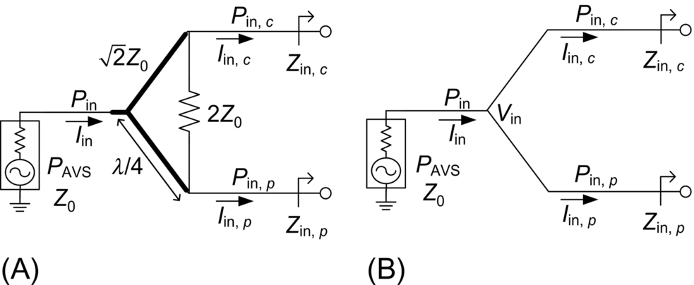
A direct input dividing can be realized using the impedance variations of the carrier and peaking amplifiers. Unlike the power dividers, the direct input power divider does not have isolation between the carrier and peaking amplifier inputs since the carrier and peaking amplifiers share the same voltage node at the input as shown in Fig. 5.10B.
When the input impedances of the amplifiers are assumed to be Zin,c and Zin,p, respectively, the power at the junction is given by

Here, PAVS is the source power. At the node, the input voltage is identical, but the input current is divided to the carrier amplifier and the peaking amplifier by the ratio of their admittances. The divided currents and the voltage at the junction determine the input powers to the carrier and peaking amplifiers, respectively. The divided powers are given by


The matched impedances of the carrier and peaking amplifiers are given by
The power-dividing ratio is equal to the ratio of the input admittances of the amplifiers:

The input impedance of the carrier amplifier remains almost constant for the input power variation, while that of the peaking amplifier changes significantly because of the class C bias. For 1: N power dividing, with the matched carrier amplifier, the transformed input impedance of the peaking amplifier is given by

where rin and xin are normalized by Z0. Eq. (5.10) becomes

which is an equation of a circle centered at r = 1/(2N) and x = 0, with radius of 1/(2N), and is represented by a conductance circle on the Smith chart. In the case of N = 1, rin,p and xin,p are on the Z0 conductance circle on the Smith chart. Fig. 5.13B shows a power-dividing ratio contours according to the trace of Zin,p, where Zin,c is matched to Z0. Fig. 5.15 shows the input impedances of the peaking amplifier for 1:1 dividing for the even drive and 1:2 dividing for the uneven drive. When Zin,p is located inside of the 1:1 circle, the uneven drive is realized, delivering more power to the peaking amplifier. Following Zin,p matched by the HPF circuit shown in Fig. 5.12, the trace of the uneven Pin drive is depicted in Fig. 5.15. The trace indicates that the carrier amplifier receives more power at a low-input-power region and the peaking amplifier gets more power at a high-input-power region, which is the desired input drive.

5.3.1.3 Realization of the Input Power Dividing Circuit
The phase compensation network of the quarter-wavelength line at the input of the peaking amplifier as shown in Fig. 5.9A can perturb the proper input power dividing. Alternatively, the phase compensation network is employed at the input of the carrier amplifier using a HPF-type circuit with negative angle as shown in Fig. 5.16. A quarter-wavelength line for the phase compensation is implemented in a lumped π-type network using two shunt inductors considering the rearrangement. The amplifiers are matched using the HPF-type matching circuit for the uneven drive. The five inductors shown in Fig. 5.16 can be merged into two inductors, and both the number and size of the inductors are reduced owing to the parallel structure. Lm1 and Lm2 are easily implemented by a collector bias line of the drive stage and a bond wire, respectively. Overall, two capacitors (Cip1 and Cic2) and one π-circuit are needed to drive the Doherty stage along with the interstage matching.

5.3.2 Output Circuit Implementation
Fig. 5.6 shows a Doherty amplifier using a quarter-wave inverter. The output capacitances of the carrier (Cout,c) and peaking (Cout,p) are resonated out at the drain by the inductances of the bias lines Lc1 and Lp1, respectively. Therefore, the matching circuits do not need to transfer the imaginary part of impedance, and the offset lines are not needed, achieving a smaller size circuit. The phase compensation circuit at the input of the carrier amplifier and the quarter-wave inverter at the output have phase delays of − 90° and 90°, respectively, and the phase delay between the two amplifiers are adjusted.
To implement the amplifier on a single chip for a handset application, the bulky quarter-wave inverter should be replaced by an equivalent lumped LC network as shown in Fig. 5.17. The lumped network type should be chosen carefully by considering the compact design and the harmonic load condition. In the size aspect, (A) and (B) types can share a single collector bias line, but (C) and (D) require two collector bias lines due to the DC blocking capacitor. The shunt inductors of (C) can be used for collector bias lines of the carrier and peaking amplifiers, respectively, but the inductance should be large to compensate the output capacitors Cout,c and Cout,p.

With the high-pass π type (C), both the number and values of the lumped components can be significantly reduced, similarly to the elaborated matching technique at the input that is explained in Section 5.3.1.3. However, (A) and (B) circuits have a size advantage at the output. Since the shunt capacitors of the low-pass π type (A) can be merged with the output capacitors Cout,c and Cout,p, their values and sizes are reduced. In general, an output matching circuit of a power amplifier for a handset is implemented by off-chip components on the package module to reduce the output matching circuit loss. Due to the low characteristic impedance of ROPT at ~ GHz band, the inductance of the lumped inverter is lower than 1 nH (for ROPT = 8 Ω device, Lc1 = 0.67 nH). Therefore, a series inductor of (A) can be implemented by a bond-wire inductance that is employed to connect the chip to a package module.
The lumped inverter of (A) is the most suited structure to reduce the size of the network, but the size of the harmonic load should also be considered. To analyze the circuit in detail, harmonic balance simulation with the schematic shown in Fig. 5.18 is conducted, and the results are shown in Fig. 5.19. With the lumped inverter, the second-harmonic shorts at the outputs of the carrier and peaking amplifiers have a minor effect on linearity since the large shunt capacitors Cc1 and Cc2 provide near short second-harmonic load conditions for the carrier and peaking amplifiers, respectively. Therefore, the amplifier can deliver a good IMD3 characteristic without the second-harmonic shorts.


However, the second-harmonic shorts at the outputs of the carrier and peaking amplifiers show different effects on the PAE. When the second-harmonic short is provided at the carrier amplifier, it reduces the PAE because the out-of-phase second-harmonic current is increased and bifurcated current waveforms is generated, reducing the ratio of Ic.Carrier.Fund/Ic.Carrier.DC as shown in Fig. 5.20A. On the other hand, when the second-harmonic short is provided at the peaking amplifier, it improves the PAE because the in-phase second-harmonic current is increased and the half-sinusoidal peaked current waveform is generated, increasing the ratio of Ic.Peaking.Fund/Ic.Peaking.DC as shown in Fig. 5.20B. Consequently, the peaking amplifier with the second-harmonic short delivers a higher PAE in contrast to the carrier amplifier. Therefore, the short circuit is employed only at the peaking amplifier.

5.4 Implementation and Measurement
Total schematic of the linear Doherty power amplifier and its implemented chip photograph are shown in Fig. 5.21. The power amplifier is fabricated using an InGaP/GaAs HBT, and the chip area is 1.1 × 1.2 mm2. With a supply voltage of 3.4 V, the quiescent currents of the amplifier are 24 and 36 mA for the drive and power stages, respectively. Fig. 5.22 shows the measured PAE, gain, and IMD3 of the power amplifier for a 10 MHz tone-spacing two-tone signal at 1.9 GHz. The power amplifier delivers not only good linearity but also high efficiency by using the proper harmonic control as described before. For a 10 MHz BW 16-quadrature amplitude modulation (QAM) 7.5 dB PAPR LTE signal at 1.9 GHz frequency, the power amplifier delivers a gain of 25.1 dB, a PAE of 45.8%, and an evolved universal terrestrial radio access adjacent channel leakage ratio (E-UTRAACLR) of − 35 dBc at an average output power of 27.5 dBm as shown in Fig. 5.23. Without any additional chip like an ET amplifier, this simple Doherty power amplifier delivers the high performance at the peak output power and at the PBO regions.


5.5 Doherty Power Amplifier Based on CMOS Process
In CMOS power amplifier, a differential structure based on a transformer is widely used because this architecture is well suited to solve the low breakdown voltage and low power density of a CMOS device. In this architecture, the differential output power is voltage-combined, increasing the output load impedance and providing a good virtual ground for a large transistor with a low impedance. Therefore, a voltage-combined Doherty power amplifier based on the transformer is a natural choice for the CMOS process. As shown in Section 1.4.1, the series load can be properly modulated with the output transformer. The series Doherty amplifier modulates the load exactly the same way with the conventional current combining Doherty amplifier. The only difference is the output powers from the carrier and peaking amplifiers are combined in voltage way.
5.5.1 Implementation of Linear CMOS Doherty Power Amplifier
The schematic of the CMOS Doherty power amplifier including the output transformer is shown in Fig. 5.24. The carrier and peaking amplifiers are cascode amplifiers, and they are voltage-combined using the transformer. Thick-oxide 0.4 μm gate transistors are used in the common-gate (CG) stages for reliable high-power operation, and thin-oxide 0.18 μm gate transistors are used in the common-source (CS) stages to enhance transconductance and gain. The total gate widths of the thin and thick devices are 4800 and 9600 μm, respectively. The second-harmonic short circuits implemented by metal-insulator-metal (MIM) capacitors and the inductances of a down-bonding wires are provided at the sources of the CS stages to improve linearity by providing the proper second-harmonic grounding and suppressing the second-harmonic term as described before. The RCG-CCG bias circuits are inserted to control the voltage swings at the gates of the CG stages. The Lin,c and Lin,p of the input matching networks transform the input impedances of the transistors to pure resistance of 12 Ω. A 90° high-pass T-type lumped quarter-wave transformer is inserted at the input path of the peaking amplifier to compensate the phase of the output quarter-wave inverter. A transformer is used for the balanced input drive.

At the output, the output capacitances of the devices are de-embedded in the Doherty network components without using the offset line similarly to the current combining case. Fig. 5.25A shows the output matching network of the practical CMOS Doherty power amplifier, and Fig. 5.25B illustrates how to manipulate the output capacitances of the transistors without using the offset lines.

The output capacitance of the peaking transistor, ![]() is merged into the quarter-wave inverter, a low-pass π type, considering the compact implementation. Thus, the first shunt capacitor (Cp1) is the lumped inverter capacitance subtracted by the
is merged into the quarter-wave inverter, a low-pass π type, considering the compact implementation. Thus, the first shunt capacitor (Cp1) is the lumped inverter capacitance subtracted by the![]() . The output transformer with C1 and C2 provides impedance matching for the output. Since the center tap of the output transformer is used as a biasing point for compact implementation, the output capacitance of the carrier amplifier
. The output transformer with C1 and C2 provides impedance matching for the output. Since the center tap of the output transformer is used as a biasing point for compact implementation, the output capacitance of the carrier amplifier ![]() should be 2C1 for a simple merged structure without offset line for the carrier amplifier. The C1 and Cinverter determine the second shunt capacitor (Cp2) of the lumped inverter as shown in Fig. 5.25B. A printed-circuit-board (PCB) transformer is designed using two-layer metal lines. The use of the two metal layers generates stronger coupling and has an advantage in size. The Lp1 and Cp2, which are parts of the lumped inverter, are also implemented on the PCB using the metal line and the external capacitor, respectively. The external capacitor C2 is used for the impedance matching with the small inductance of the secondary trace. The insertion loss of the output transformer including the C2 is 0.32 dB at 880 MHz.
should be 2C1 for a simple merged structure without offset line for the carrier amplifier. The C1 and Cinverter determine the second shunt capacitor (Cp2) of the lumped inverter as shown in Fig. 5.25B. A printed-circuit-board (PCB) transformer is designed using two-layer metal lines. The use of the two metal layers generates stronger coupling and has an advantage in size. The Lp1 and Cp2, which are parts of the lumped inverter, are also implemented on the PCB using the metal line and the external capacitor, respectively. The external capacitor C2 is used for the impedance matching with the small inductance of the secondary trace. The insertion loss of the output transformer including the C2 is 0.32 dB at 880 MHz.
5.5.2 Measurement Results
The power amplifier is fabricated using a 0.18 μm CMOS process, and the total chip area including the pads is 1.2 × 1.1 mm2 as shown in Fig. 5.26. The total amplifier module including the output combining transformer on an FR4 PCB board is 5.0 × 2.9 mm2. Fig. 5.27 shows the measured two-tone performance of the power amplifier with a supply voltage of 4.0 V at the 880 MHz. The first peak efficiency at the 6 dB PBO can be maximized by adjusting the CS gate bias voltage of the peaking amplifier. However, the amplifier at the gate bias with the maximized efficiency produces a gain distortion, deteriorating the linearity as shown in Fig. 5.27A. For the linear Doherty power amplifier, the CS gate bias of the peaking amplifier is chosen to make a linear AM-AM and AM-PM characteristics. With the proper CS gate biases and the additional phase delay line merged into the input phase compensation network, the Doherty power amplifier achieves low IMDs as shown in Fig. 5.27B.


The linear power amplifier is tested at 880 MHz using a 10 MHz BW, 16-quadrature amplitude modulation (QAM) and 7.5 dB PAPR LTE signal, and the results are shown in Fig. 5.28. The power amplifier delivers a gain of 13.3 dB, a PAE of 47.4%, an error vector magnitude (EVM) of 3.85%, and an E-UTRAACLR of − 33 dBc at an average output power of 27 dBm. Without using any complex circuitry, the CMOS Doherty power amplifier based on a voltage-combining method could deliver the very good performance for the LTE signal with large PAPR.

5.6 Average Power Tracking Operation of the Handset Doherty Amplifier
The power amplifier for a handset application should operate efficiently over a large dynamic range, since the power requirement varies with the distance between a base station and a user equipment. Even for the base-station power amplifier, the power control is needed according to the user traffic as described in Section 3.5. Due to the recent trend of multimode operation, one power amplifier should cover the 3G and 4G modulation standards. By referring to the statistical probability density function (PDF) of the output power for the 3G wideband code division multiple access (WCDMA) system, the probability of transmission at higher than 17 dBm is statistically below 2%, and the power amplifier mostly operates at a back-off power. Also, for the 4G long-term evolution (LTE), the power amplifier spends about 50% of its duration at the back-off power level. As the average output power is decreased, the Doherty power amplifier delivers still a low efficiency. Therefore, the Doherty power amplifier needs to be reconfigured properly for the variation of the average output power. For the purpose, a linear power amplifier with average power tracking (APT) is popularly employed in the handset power amplifier and a similar technology can be applied to the Doherty power amplifier.
For the APT operation of a Doherty amplifier, a multilevel DC-DC converter should be linked to all amplifiers including the carrier, peaking, and drive amplifiers. The cancellation of the IM3s between the carrier and peaking amplifiers is the most important design issue in realization of a linear Doherty power amplifier with APT. However, the IM3 cancellation couldn't be maintained through the various collector biases, deteriorating the linearity. To solve the problem, the base biases of the carrier and peaking amplifiers should be adapted properly to achieve a high linearity for the collector bias sweep.
5.6.1 Adaptive Base Bias Control Circuit for Average Power Tracking
Fig. 5.29A shows the schematic of the two-stage Doherty power amplifier. A direct input-power-dividing technique is employed to optimize the load modulation through a proper input drive and to reduce number of circuit components at the input. Flat AM-AM and AM-PM responses are achieved at all power levels by analysis of the gain modulation and selection of proper base biases. To improve the linearity and reduce the size, the lumped quarter-wave transformer of a low-pass π type is selected at the output of the carrier amplifier, and the second-harmonic short circuit is employed at the peaking amplifier only.

Fig. 5.30 shows the measurement results with a two-tone signal at 1.9 GHz having 10 MHz tone-spacing. The Doherty power amplifier delivers a good linearity under − 30 dBc with 3.4 V Vcc. However, the linearity is worsen as Vcc is decreased. With the voltage lower than 2.4 V Vcc, the power amplifier does not meet the − 30 dBc linearity specification. This means that the IM3 can be cancelled optimally only at the fixed Vcc, and the circuit should be retuned for proper IM3 cancellation at the different Vcc.

Since the load is fixed, as the collector bias of the carrier and peaking amplifiers is decreased, the peak output power of the Doherty power amplifier is decreased. Therefore, the input power should be reduced as the peak output power is decreased. Therefore, the carrier amplifier is operated in the low-current region with the low base current, and the base bias of the carrier amplifier should be reduced. To maintain the good linearity with the Vcc variation, the turn-on time of the peaking amplifier should be properly adjusted since the linearity at the 6 dB back-off region is closely related to the cancellation of the IM3 components generated by the carrier and peaking amplifiers. The peaking amplifier should be turned on at a 6 dB back-off level from the lower input power. To maintain the turn-on timing at the optimum back-off level, the base bias of the peaking amplifier needs to be increased because the threshold voltage of a transistor does not change much with the collector bias sweep.
The simulated optimum base currents of the carrier and peaking amplifiers to maintain the linearity at the high-power region with the Vcc sweep are depicted in Fig. 5.31. As shown, the carrier current should be reduced linearly as the collector bias is reduced. However, the peaking current is increased with the reduced voltage. The adaptive circuits suitable to control the base current levels of the carrier and peaking amplifiers are shown in Fig. 5.32. The control voltage of the adaptive bias circuits is supplied from the output voltage of the multi-level DC-DC converter (Vout.APT). The adaptive bias circuits automatically generate the extracted optimum base bias points of the carrier and peaking amplifiers, respectively, as shown in Fig. 5.31. As explained, the optimum bias point of the carrier amplifier is decreased and that of the peaking amplifier is increased, as the collector bias is decreased.


5.6.2 Implementation and Measurement
The Doherty power amplifier is fabricated using an InGaP/GaAs HBT and the chip area is 1.25 × 0.95 mm2, as shown in Fig. 5.29B. Texas Instruments' LM3290 product is used for the multilevel DC-DC converter. Its output voltage ranges are from 0.4 to 3.81 V, and the highest efficiency is 95% with Vout.APT of 3.81 V. Fig. 5.33 shows the measured performance of the Doherty power amplifier with various Vout.APT at 1.9 GHz for a 10 MHz BW 16-quadrature amplitude modulation (QAM) 7.5 dB PAPR LTE signal. The power amplifier with Vout.APT of 3.8 V delivers a gain of 24.4 dB, a PAE of 45.7%, an error vector magnitude (EVM) of 2.65%, and an evolved universal terrestrial radio access adjacent channel leakage ratio (E-UTRAACLR) of − 35.3 dBc at an average output power of 27.5 dBm. The Doherty power amplifier with the APT shows a high efficiency at overall dynamic ranges for various Vout.APT from 1.0 to 3.8 V. The E-UTRAACLR specifications are satisfied for all Vout.APT having more than − 5 dBc margin. In comparison with the Doherty power amplifier with the ideal APT, the efficiency of the power amplifier with the APT is slightly lower due to the limited efficiency of the multilevel DC-DC converter as shown in Fig. 5.34. However, the efficiency at the whole back-off regions is significantly improved from the Doherty power amplifier with a fixed bias.

