
Advanced Architecture of Doherty Amplifier
Abstract
When the Doherty amplifier is designed based on the identical two amplifiers, the first peak-efficiency point is located at the fixed 6 dB back-off power. However, to get a higher efficiency for amplification of the highly modulated signal, the point should be located at a larger back-off point, or the efficiency can be even higher by increasing the number of the maximum efficiency points. These behaviors can be achieved from the N-way Doherty amplifier and the N-stage Doherty amplifier. The design methods and the problems for implementation of these amplifiers are discussed. It is also shown that the N-way Doherty amplifier can be used as a highly linear amplifier by tuning the multiple cells for accurate harmonic cancellation.
Keywords:
Three-way Doherty amplifier; Three-stage Doherty amplifier; Efficiency; Linearity; Load modulation; Impedance transformation
So far, we have considered the Doherty amplifier based on two identical amplifiers. In this case, the first peak-efficiency point is located at the fixed 6 dB back-off power. However, according to the modulated signal profile, the location of the peak point should be changed to get a higher efficiency for amplification of the signal, or the efficiency can be even higher by increasing the number of the maximum efficiency points. These behaviors can be achieved by increasing the number of the unit amplifiers, one carrier amplifier and (N − 1) peaking amplifiers. When the (N − 1) unit amplifier cells are used for the peaking amplifier with one load-modulation circuit, which is called N-way Doherty amplifier, the back-off level for the first peak-efficiency point is increased accordingly. When the (N − 1) unit amplifier cells are used for the peaking amplifier and the cells modulate the load sequentially using the separate load-modulation circuits, the number of the peak-efficiency points is increased accordingly and is called N-state Doherty amplifier. These amplifiers can deliver a higher efficiency for amplification of a highly modulated signal. The N-way Doherty amplifier can be used as a highly linear amplifier by tuning the multiple cells for accurate harmonic cancellation. The design concepts of these amplifiers are described in this chapter.
4.1 N-Way Doherty Amplifier
The two-way Doherty amplifier, the basic architecture of the Doherty amplifier we have discussed so far, has two identical unit amplifiers for the carrier amplifier and peaking amplifier and has two maximum efficiency points at the 6 dB back-off output power and the peak output power. The multiway Doherty amplifier consists of N identical unit cells, one cell for the carrier amplifier and (N − 1) cells for the peaking amplifier, and is called a multi (in this case N)-way Doherty amplifier. The total size of the peaking amplifier (1 ~ N − 1) compared with that of the carrier amplifier determines the back-off output power level for the maximum efficiency point. The efficiency between the two peak-efficiency points, however, drops further as the separation between the two points increases. This architecture is useful for adjusting the first peak-efficiency power point closer to the average power region, which is required for efficient amplification of a signal with a high peak-to-average power ratio (PAPR).
4.1.1 Load Modulation of N-way Doherty Amplifier
Fig. 4.1 shows an equivalent circuit model of the N-way Doherty amplifier with N identical ideal current sources. Ic, Ic′, and Ip represent the drain current of the carrier amplifier, the current after the inverter, and the drain current of the unit peaking cell, respectively. Since the inverter is lossless, a constant power flows through the inverter. Therefore, Ic′ can be calculated from the constant power flow concept:
I′c=Ic⋅√ZcZ′c=Ic⋅R0Z′c=Ic⋅ZcR0


The load modulation is carried out by the current ratio between the carrier amplifier and peaking amplifier, and the load impedances of the unit cells can be derived by the load-modulation principle described in Chapter One:
V0=R0N⋅(I′c+Ip,Total)=R0N⋅(I′c+N−1∑1Ip)

Z′c=V0I′c=R0N(1+∑N−11IpI′c)=R0(N−∑N−11IpIc)

Zc=R02Z′c=R0(N−∑N−11IpIc)

ZP=V0Ip=R0NIp⋅(I′c+N−1∑1Ip)=R0⋅Ic√Ip(NIc−∑N−11Ip)

In Eqs. (4.4), (4.5), Zc and Zp are the load impedances of the carrier cell and peaking unit cell, respectively.
If the current ratio of the peaking cell to the carrier cell is α, the load impedances of the unit cells, for a given input drive Vin, can be written as follows:
α(Vin)=Ip(Vin)Ic(Vin)

Zc=R0⋅[N−α(Vin)(N−1)]
ZP=R0√α(Vin)⋅[N−(N−1)α(Vin)]

Since the unit cells are identical, α should be changed from 0 to 1 according to the input power level. The peaking amplifier should be turned on at the input voltage of Vmax/N, where Vmax is the maximum input voltage swing and the transconductance of the peaking cell should be larger than that of the carrier amplifier by 1 + 1/N. Because of the early turn-on of the N-way peaking amplifier, the uneven drive problem is reduced compared with the standard Doherty amplifier.
Accordingly, the load impedances are modulated with α(Vin) as follows:
Zc={N⋅R0,atVin=VmaxNwithα(Vin)=0R0,atVin=Vmaxwithα(Vin)=1

ZP={∞,atVin=VmaxNwithα(Vin)=0R0,atVin=Vmaxwithα(Vin)=1

Since all the peaking cells are modulated in the same way, the total impedance of the peaking amplifier is reduced by 1/(N − 1) due to the parallel connection of the cells. The impedance of the carrier amplifier is increased in proportion to N when the peaking amplifier is turned off. At the peak power, all the cells see the same load impedance of R0.
Fig. 4.2 shows the load-modulation behaviors of the two-way Doherty amplifier and three-way Doherty amplifier. As shown in the above analysis, the peaking cells of the three-way Doherty amplifier are turned on at one-third of the maximum input voltage swing, and the load impedance of the cells is modulated from open to R0. The load impedance of the carrier amplifier is modulated from 3R0 to R0 as the peaking amplifier generates the current from zero to the maximum value. It should be remembered that the peaking amplifier has (N − 1) unit cells and the total current of the peaking amplifier is (N − 1) times larger than Imax.

The load lines of the carrier and peaking amplifiers are illustrated in Fig. 4.3. Before the peaking amplifier turns on, the carrier amplifier operates as a single class B amplifier. When the carrier amplifier reaches to the maximum efficiency point, the peaking amplifier is turned on. After turned on, the load impedance of the carrier amplifier is modulated, and the load line always follows the saturated region, generating the maximum efficiency as explained in Chapter One. The load impedance of the peaking amplifier is also modulated, but the amplifier delivers the peak efficiency only at the maximum output power point. For the load lines, it is assumed that transconductance of the peaking cell is N/(N − 1) times larger than that of the carrier amplifier. Therefore, the amplifiers reach the maximum current level simultaneously although the peaking amplifier is biased lower. It can be achieved using a bigger-size device for the peaking cells, but in real design, the same-size devices are employed to fully utilize the precious device resource, resulting in deviation from the ideal behaviors. This problem can be solved by the uneven drive or gate-bias adaptation, which is discussed in Chapter Two.

4.1.2 Efficiency of N-Way Doherty Amplifier
Using Eqs. (4.7), (4.8), the efficiency variation of the Doherty amplifier with the input power level can be derived. For the analysis, the transconductances of the devices are assumed to be uniform, generating the fundamental current components linearly with the input voltage as shown in Fig. 4.4. The carrier amplifier and peaking amplifier are operated at class B mode with the different turn-on voltages. The currents of the two amplifiers are given by
Ic(Vin)=VinVmax⋅Imax

Ip(Vin)={0,for0<Vin<VmaxNImax⋅(N⋅VinVmax−1),forVmaxN<Vin<Vmax


Here, Imax is the maximum current of the single cell.
For the input voltage level of 0≤vin<VmaxN![]() , the RF and DC powers can be calculated as follows:
, the RF and DC powers can be calculated as follows:
PRF(vin)=18⋅IC(vin)2⋅ZC(vin)=Imax28⋅(vinVmax)2⋅R0⋅[N−α(Vin)(N−1)]=N⋅Imax⋅Vdc4⋅(vinVmax)2(where,α(vin)=0for0≤vin<VmaxN)

PDC(vin)=Vdc⋅Idc(vin)=Vdc⋅1π⋅Imax⋅(vinVmax)

At the input level of Vmax/N ≤ vin < Vmax, the RF and DC powers are given by
PRF(vin)=18⋅IC(vin)2⋅ZC(vin)+18⋅IP(vin)2⋅ZP(vin)=Imax28⋅(vinVmax)2⋅R0⋅[N−α(Vin)(N−1)]+Imax28⋅(VinVmax⋅N−1)2⋅R0√α(Vin)⋅[N−(N−1)α(Vin)]=14⋅Imax⋅Vdc⋅[(vinVmax)2⋅[N−α(Vin)(N−1)]+(VinVmax⋅N−1)2⋅1√α(Vin)⋅[N−(N−1)α(Vin)]]

PDC(vin)=Vdc⋅[Idc(vin)+(N−1)⋅Idp(vin)]=1π⋅Imax⋅Vdc⋅[vinVmax+(VinVmax⋅N−1)]

The efficiency can be calculated from Eqs. (4.13) to (4.16).
η={π4⋅N⋅vinVmax,0≤vin<VmaxNπ4⋅[(vinVmax)2⋅[N−α(Vin)(N−1)]+(VinVmax⋅N−1)2⋅1√α(Vin)⋅[N−(N−1)α(Vin)]]vinVmax+(VinVmax⋅N−1)VmaxN≤vin<Vmaxπ4vin=Vmax

Fig. 4.5 shows the calculated efficiency of the N-way Doherty amplifier versus the output power level calculated by Eq. (4.17). The maximum efficiency of 78.5% (π/4) is obtained at the input power levels of “Vmax/N” and “Vmax.” The output power level for the first peak-efficiency point is 1/N2 or 20·log (1/N) dB down from the peak output power. The back-off power level for the maximum efficiency is increased as the size of the peaking amplifier (number of peaking cells) is increased. The three-way and four-way Doherty amplifiers deliver the maximum efficiencies at the back-off powers of 9.54 dB (1/9 of normalized output power) and 12 dB (1/16 of normalized output power), respectively. The efficiency between the two power points is decreased as the separation is increased.
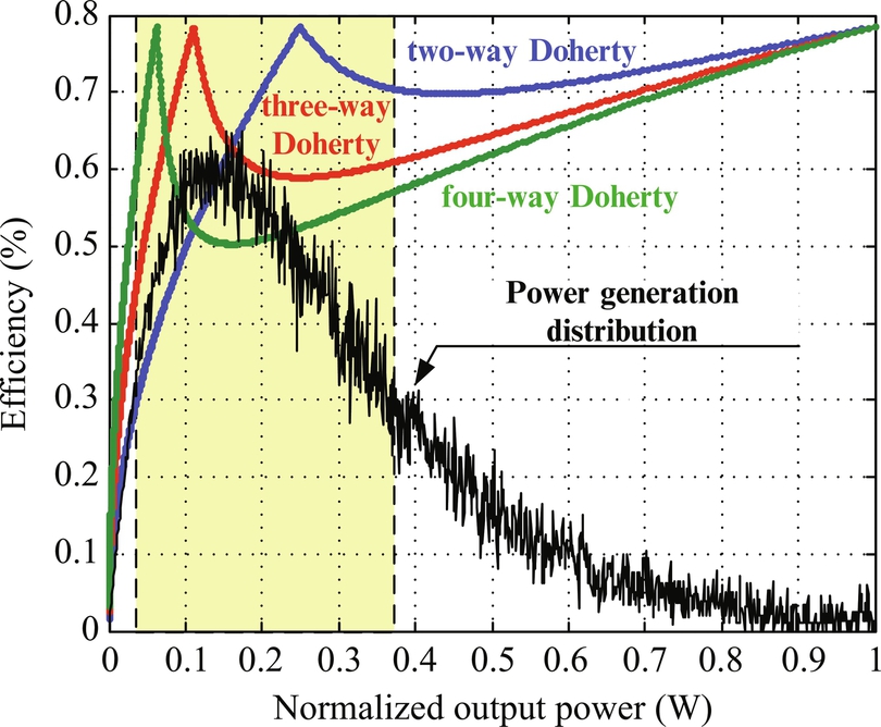
To evaluate the efficiency of the Doherty amplifier for amplification of a modulated signal, the 802.16e Mobile WiMAX signal with 8.5 dB PAPR is used. The drain efficiency (DE) of N-way Doherty amplifier for the modulated signal is determined by following equation:
DE=∫prob.(vin)⋅Pout(vin)dvin∫prob.(vin)⋅Pdc(vin)dvin

The prob.(vin) is the occurrence probability of the vin in the modulated input signal. The overall DE is determined by ratio of the multiplications of the probability distribution and power generation terms (Pout) over the multiplications of the distribution and DC power (Pdc). The numerator in Eq. (4.18) is named as the power generation distribution (PGD) of the signal, which represents the real power generation at the input level of the modulated signal. The normalized power generation amount is also shown in Fig. 4.5. The average power generation point is 7.5 dB lower than the peak power for 802.16e mobile WiMAX signal with 8.5 dB PAPR. The distribution indicates that the dominant power generation region for amplification of the modulated signal is 0.03 ~ 0.37, indicating that three-way Doherty amplifier is the best suited one. According to the PAPR of the modulated signal, the important power generation region indicated by the PGD is changed, and the N-way Doherty amplifier should be chosen properly according to the distribution. The calculated DEs for the N-way Doherty amplifiers are summarized in Table 4.1.
Table 4.1
| Two-Way | Three-Way | Four-Way | |
|---|---|---|---|
| ηavg (%) | 59.5 | 62 | 56.5 |

The calculated DEs for the signal with various PAPRs are illustrated in Fig. 4.6. Because the back-off level of PGD is lower than that of PAPR, the two-way Doherty amplifier delivers the highest efficiency for the signal with PAPR of up to 7.5 dB, and the three-way is better for the higher PAPR signals.
The N-way Doherty amplifier is not the optimum architecture for an efficient transmitter because it does not maintain the peak efficiency at the important PGD region. These low-efficiency regions are originated from the unsaturated operations of the carrier amplifier at the low-power region and the peaking amplifier at the high-power region. To reduce the efficiency degradation, the high-efficiency characteristic should be maintained over the important PGD region. It can be achieved by increasing the number of the maximum efficiency points by increasing the load-modulation networks (N), and the N-stage Doherty amplifier has been suggested. At the next section, we will explore the N-stage Doherty amplifier for the highly efficient amplification of a signal with a high PAPR.
4.1.3 Linearity of N-way Doherty Amplifier
As discussed in Chapter One, the Doherty amplifier is inherently a linear power amplifier if the internal distortions generated by the carrier and peaking amplifiers are not considered. To realize a linear Doherty amplifier, the distortions should be minimized. For a linear Doherty amplifier, the carrier amplifier is biased at class AB and the peaking amplifier at class C. The class AB carrier amplifier should operate linearly by itself at the low power before the peaking amplifier turns on. At near or above the first peak-efficiency point, the carrier amplifier operates at the near-saturation mode, and a large distortion is generated from the carrier amplifier. The distortion at the saturated operation should be canceled by the distortion generated by the class C biased peaking amplifier. It is possible since the class AB mode carrier amplifier has a gain compression characteristic while the class C mode peaking amplifier has a large gain-expansion characteristic. By adjusting the two gain characteristics through the proper gate biases of the two amplifiers, a constant gain from the Doherty amplifier can be obtained. It is equivalent to cancellation of the harmonic distortions generated by the two amplifiers. The asymmetrical output powers from the carrier and peaking amplifiers with the adjusted biases are combined by the Doherty network, which is a very nice unique characteristic of Doherty amplifier.
The nonlinear output current of an active device can be expressed using Taylor series expansion by
Iout=gm1⋅vin+gm2⋅vin2+gm3⋅vin3+gm4⋅vin4+gm5⋅vin5+⋯
where vin is the input gate voltage and gmX's are the Xth-order expansion coefficients of the nonlinear gm. The third-order intermodulation IM3 current is mainly generated by gm3⋅vin3![]() term and the fifth-order intermodulation IM5 current by gm5⋅vin5
term and the fifth-order intermodulation IM5 current by gm5⋅vin5![]() term in Eq. (4.19). For a sinewave input to Eq. (4.19), the fundamental component Ioutfund is given by
term in Eq. (4.19). For a sinewave input to Eq. (4.19), the fundamental component Ioutfund is given by
Ioutfund=[gm1⋅vin+94gm3⋅vin3+254gm5⋅vin5+⋯]

Fig. 4.7 presents gm3 curve according to the gate-bias voltage of a transistor. It is important to notice that gm3 is positive for the gate bias close to the pinch off and is negative for the higher bias voltage. Because of the positive gm3, the class C amplifier has a gain-expansion characteristic since this IM3 can generate the fundamental term as shown in Eq. (4.20), while the class AB amplifier with the negative gm3 has a gain compression characteristic.

As mentioned earlier, for a linear Doherty amplifier, the carrier amplifier is biased at a class AB mode and should operate linearly by itself. The bias voltage of the peaking amplifier should be in class C mode in order to have proper positive gm3 necessary for canceling the IMD3 current generated by the class AB carrier amplifier at a high power operation with near saturation. This class C peaking amplifier generates a considerable amount of the higher-order intermodulation terms, especially the fifth-order terms. However, a linear two-way Doherty amplifier can be realized by using this harmonic cancellation mechanism, and we will discuss this amplifier in Chapter Five “Linear Doherty Amplifier for Handset Application”
For the three-way case, which has two peaking cells, an extremely linear Doherty amplifier can be realized. For the amplifier, the required bias voltage for the proper IMD3 cancellation is higher than the two-way Doherty amplifier. Therefore, the peaking amplifiers operate more linearly without generating the excessive higher-order distortion terms, helping for linear operation. The gate bias of the higher-way Doherty amplifier should be even higher, but the higher-bias operation more than the three-way Doherty amplifier increases the sensitivity for the harmonic cancellation. Consequently, the best efficiency versus linearity characteristics should be considered.
The two-, three-, and four-way Doherty amplifiers are compared for their performances on linearity and efficiency. The basic amplifier cells have been designed using Motorola's 4 W PEP silicon LDMOSFET. The linearity is optimized by adjusting the gate biases of the peaking cells. The uneven powers from the two amplifiers are automatically combined by the load-modulation circuit. The class AB amplifiers for the reference points are realized by equally AB biasing all the unit cells of the Doherty amplifier. Fig. 4.8A shows the measured ACLRs of the two-way Doherty amplifier and class AB amplifier at 2.5 MHz offset and 5 MHz offset for one- and two-carrier downlink WCDMA signals (5 MHz bandwidth), respectively. For the one-carrier WCDMA signal, ACLR is improved by 4.69 dB at an output power of 27 dBm. Fig. 4.8B shows the measured PAEs of the two-way Doherty and class AB amplifiers for the one- and two-carrier downlink WCDMA signals. The PAE is improved by 6.45%, from 21.45% to 27.9% at the output power of 32 dBm. The optimized quiescent current of the peaking amplifier is 0.1 mA, while those of the carrier amplifier and the class AB amplifiers are 60 mA.

Fig. 4.9A shows the measured ACLRs of the three-way Doherty and class AB amplifiers. For the one-carrier WCDMA signal, ACLR is improved by 9.97 dB at the output power of 30 dBm. Fig. 4.9B shows the measured PAEs of the three-way Doherty and class AB amplifiers. The PAE is improved slightly by 1.98% at an output power of 34 dBm.

Fig. 4.10A shows the measured ACLRs of the four-way Doherty and class AB amplifiers. For the one-carrier WCDMA signal, ACLR is improved by 8.83 dB at an output power of 32 dBm. Fig. 4.10B shows the measured PAEs of the four-way Doherty and class AB amplifiers. The PAE is improved by 2.5% at output power of 35 dBm. The optimized quiescent currents of the peaking amplifiers are 12.8 and 15.73 mA for the three- and four-way cases, respectively.

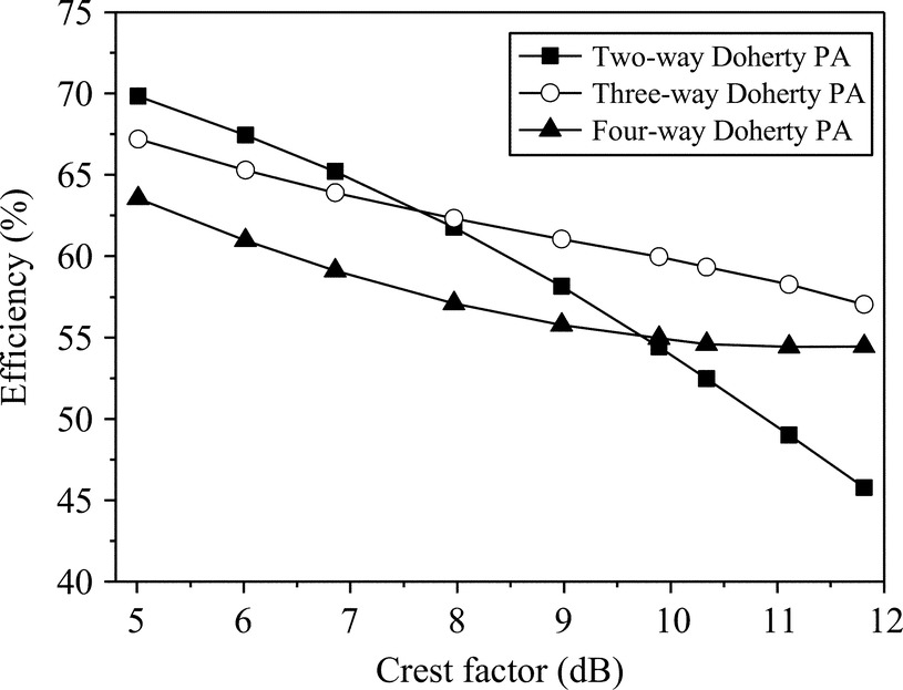
As shown, the three- or four-way Doherty amplifiers deliver greatly improved linearity over the two-way Doherty amplifier. However, for the four-way case, the linearity improvement is observed over a relatively narrow output power range compared with the three-way case, which means that the excessive numbers of the peaking cells make the IM3 cancellation very sensitive. Also, as the number of peaking cells is increased, the bias current is also raised for the intermodulation cancellation. Therefore, the load-modulation effect is reduced, and the efficiency is reduced, comparable with the class AB operation. Fig. 4.11 compares the data for the efficiency and linearity characteristics of the amplifiers. Compared with the normal class AB operated amplifiers, the N-way Doherty amplifiers deliver much more improved efficiency versus linearity. The two-way shows the best efficiency above − 35 dBc of ACLR, while the three-way shows best efficiency below − 41 dBc. For the intermediate region, the four-way shows slightly better efficiency than that of the three-way.

As shown, the three-way Doherty amplifier can be very linear, and the linearity can be further enhanced. To maximize the linearity of the amplifier, the carrier amplifier is designed to be very linear by biasing at near class A mode, and the biases of the peaking cells are adjusted for the IMD3 and IMD5 cancellations. The three-way Doherty amplifier has been implemented using three Motorola's MRF21060 (60 W PEP) LDMOSFETs at 2.14 GHz. In the experiments, the quiescent drain currents of the carrier and peaking amplifiers are set to 700 mA at VDD = 28 V for the class AB amplifier operation. For the three-way Doherty amplifier, the quiescent drain current of the carrier amplifier is set to 820 mA at VDD = 28 V, but the peaking cells are biased at class AB mode, around 260, 280 mA, respectively with VDD = 28 V. Fig. 4.12 shows the measured ACLRs and PAEs of the class AB amplifier and three-way Doherty amplifier. Fig. 4.12A is for one-carrier WCDMA signal with 10 MHz bandwidth, and Fig. 4.12B is for two-carrier WCDMA signal with 10 MHz spacing. The three-way Doherty is very linear with ACLR of under 50 dBc. For the one-carrier WCDMA signal, ACLR is improved by about 10 dB compared with the class AB amplifier. The PAE is improved slightly by about 2% at the same output power. For the two-carrier WCDMA signal, ACLR of the three-way Doherty is improved by 6.8 dB at an output power 40 dBm, and the improvement of the PAEs is similar to the one-carrier case. Fig. 4.13 explains the linearity boosting mechanism of the three-way Doherty. For the three-way Doherty amplifier, the IMD3 and IMD5 are reduced simultaneously compared with the class AB case.


In summary, the gate-bias voltages of the two cells of the peaking amplifier can be adjusted to cancel the IMD3 more accurately, and the peaking amplifier itself operates more linearly due to the higher gate bias. In this operation, the efficiency can be relatively high due to the near-normal Doherty operation. For the very linear operation, the three and fifth harmonics should be canceled using the two peaking cells. Since the fifth harmonic level is around 40–45 dBc, without the fifth harmonic cancel, the linearity cannot reach below − 50 dBc. In this operation, the amplifier is very linear, but the efficiency is not high.
4.2 Three-Stage Doherty Amplifier
The N-way Doherty amplifier creates two maximum efficiency points with different back-off power level using different-size devices for the carrier and peaking amplifiers. On the other hand, the N-stage Doherty amplifier generates N maximum efficiency points along the output power level using (N − 1) peaking cells with (N − 1) load-modulation circuits. Therefore, the N-stage Doherty amplifier maintains the high-efficiency characteristics over a broad power range compared with the N-way Doherty amplifier. The back-off levels, where the N-stage Doherty amplifier delivers the maximum efficiency, are adjusted by the number of stages and the size ratios of the carrier amplifier and peaking amplifiers. Since the modulation circuits are turned on sequentially, the gate-bias voltages of the later turned-on stages are very low, creating the severe current generation problem.
There are two kinds of three-stage Doherty amplifier architectures. One topology (three-stage I) consisted of a carrier amplifier based on a conventional Doherty amplifier and one more peaking amplifier. The other topology (three-stage II) has one carrier amplifier, and one peaking amplifier consisted of a conventional Doherty amplifier. For the three-stage I Doherty amplifier, initially, the carrier Doherty amplifier operates like a conventional Doherty amplifier. At a higher power, the additional peaking amplifier is turned on and modulates the load of the carrier Doherty amplifier. The other topology (three-stage II) operates similarly. At a low power, only the carrier amplifier is turned on, and at higher power, the peaking Doherty amplifier, which is a conventional Doherty by itself, is turned on similarly to the conventional Doherty amplifier. Both the three-stage and the three-way architectures use three unit cells, but the two peaking cells in the three-stage Doherty amplifier are sequentially turned on, while the peaking cells of the three-way Doherty amplifier are simultaneous turned on. Thus, three peak-efficiency points are formed for the three-stage II amplifier: at the two peaking turn-on points and at the peak power. The behaviors of the three-state Doherty amplifiers will be described in this section.
4.2.1 Three-Stage I Doherty Amplifier
The conventional three-stage Doherty amplifier architecture, that is widely known for a long time and we call “three-stage I”, is shown in Fig. 4.14. The topology is one Doherty amplifier as a carrier amplifier with one additional peaking amplifier; initially, the carrier Doherty amplifier operates like a conventional Doherty amplifier, and at a higher power, the additional peaking amplifier turns on and modulates the load. It has two inverters for the sequential load modulation. The N-stage Doherty amplifier has N − 1 peaking cells with N − 1 inverters.

4.2.1.1 Fundamental Design Approach
To evaluate the back-off levels where the three-stage I Doherty amplifier delivers the maximum efficiencies, the fundamental current profiles of the cells can be defined as shown in Fig. 4.15. It should be noticed that the current of the carrier amplifier is saturated since a proper solution could not find without the saturated operation. The maximum output power of the three-stage I Doherty amplifier is given by the total output current and DC drain bias voltage, Vdc:
POut,max=12⋅Vdc⋅IOut

The maximum fundamental currents of the unit cells (carrier cell, peaking cell 1, and peaking cell 2), IC,F, IP1,F, and IP2,F, follow their sizes:
IC,F:IP1,F:IP2,F=1:m1:m2
IOut=IC,F+IP1,F+IP2,F=IC,F⋅(1+m1+m2)=IP1,F⋅(1+m1+m2)/m1=IP2,F⋅(1+m1+m2)/m2

From Eqs. (4.23), (4.21), the current levels are determined as
IC,F=2⋅POut,maxVdc⋅(1+m1+m2)

IP1,F=2⋅m1⋅POut,maxVdc⋅(1+m1+m2)

IP2,F=2⋅m2⋅POut,maxVdc⋅(1+m1+m2)

The fundamental output current amplitudes at each back-off output power level with the maximum efficiency, as shown in Fig. 4.15, are calculated. The current levels at the first back-off point are given by
IC,B1=IC,F=2⋅POut,maxVdc⋅(1+m1+m2)

IP1,B1=k1−k21−k2⋅IP1,F=k1−k21−k2⋅2⋅m1⋅POut,maxVdc⋅(1+m1+m2)

IP2,B1=0
where k1 and k2 are the turn-on voltages at the peak-efficiency points as indicated in Fig. 4.15. The current levels at the second back-off point are given by
IC,B2=k2k1⋅IC,F=k2k1⋅2⋅POut,maxVdc⋅(1+m1+m2)

IP1,B2=IP2,B2=0
Thus, the back-off output power levels are given by
POut,B1=12⋅Vdc⋅IC,B1+12⋅Vdc⋅IP1,B1
POut,B2=12⋅Vdc⋅IC,B2
Eqs. (4.30), (4.31) can be represented in different expressions using the maximum output power in Eq. (4.21), assuming that the power is linearly increased with the input power:
POut,B1=k12⋅POut,max
POut,B2=k22⋅POut,max
Using Eqs. (4.30)–(4.33), the back-off voltage levels of the three-stage I Doherty amplifier, k1 and k2, are derived as
k2=1+m11+m1+m2,k1=11+m1

As shown in Eq. (4.34), the back-off level of the three-stage I Doherty amplifier can be selected by changing the size ratios between the carrier cell and the peaking cells. Under the same assumption used previously that all of the cells are at class B mode after turned on and have proper transconductances, the fundamental currents of the unit cells can be calculated as functions of the input voltage using Eq. (4.34):
I1,C(vin)=IC,F⋅vink1⋅Vmax,=IC,F,0<vinVmax<k1k1<vinVmax<1

I1,P1(vin)=0,0<vinVmax<k2=IP1,F1−k2⋅[vinVmax−k2],k2<vinVmax<1

I1,P2(vin)=0,0<vinVmax<k1=IP2,F1−k1⋅[vinVmax−k1],k1<vinVmax<1

All of the unit cells are matched to the load impedance of R0 when the cells deliver their full powers. At the junction, the voltage is the same for all the cells, and the impedances should be the root square of the inverse of their currents. From the property, the characteristic impedances of the quarter-wavelength transmission lines, which form the three-stage Doherty I amplifier's output combiner shown in Fig. 4.14, are determined as follows:
Z01=R0⋅√m21+m1+m2

Z02=R01+m1⋅√m1⋅m2

Z03=R0⋅√m1
4.2.1.2 Load Modulation, Efficiency and Output Power
For the analysis of the load-modulation and efficiency characteristics, the ideal current source models of the Doherty amplifier shown in Fig. 4.16 can be used. At the region of “0 ~ k2,” only the carrier amplifier operates, and at the region of “k2 ~ k1,” the carrier cell and peaking cell 1 operate. All of the cells are turned on at the region of “k1 ~ 1.”

In Fig. 4.16A, the current source model of the three-stage I Doherty amplifier at the region of “0 ~ k2” is shown. The load impedance at the current source of the carrier amplifier can be derived as
∴RC,~k2(vin)=Z012⋅Z032Z022⋅R0

The drain efficiency below the second back-off region can be calculated using the RF power and DC power that are given by
PRF,~k2(vin)=12⋅I1,C(vin)2⋅RC,~k2(vin)=12⋅IC,F2⋅(vink1⋅Vmax)2⋅Z012⋅Z032Z022⋅R0=12⋅IC,F⋅Vdc⋅(vink1⋅Vmax)2⋅(Z01⋅Z03Z02⋅R0)2

PDC,~k2(vin)=IDC,C(vin)⋅Vdc=2π⋅I1,C(vin)⋅Vdc=2π⋅IC,F⋅vink1⋅Vmax⋅Vdc

DE,~k2(vin)=PRF(vin)PDC(vin)=π4⋅(vink1⋅Vmax)⋅(Z01⋅Z03Z02⋅R0)2

Fig. 4.16B represents the region of “k2 ~ k1,” where carrier cell and peaking cell 1 deliver their fundamental currents to the load. The fundamental drain current ratio provided by the carrier cell and peaking cell 1 is defined as
∴δ1(vin)=I1,P1(vin)I1,C(vin)

The load impedances at the voltage nodes shown in Fig. 4.16B can be calculated using the active load-pull principle:
RT1,~k1=Z022Z012⋅R0

RC,~k1(vin)=Z032[1+δ1(vin)]⋅RT1,~k1=Z012⋅Z032Z022⋅R0⋅[1+δ1(vin)]

RP1,~k1(vin)=[1+1δ1(vin)]⋅Z022Z012⋅R0

The drain efficiency below the first back-off region can be calculated the same way with the previous case:
PRF,~k1(vin)=12⋅I1,C(vin)2⋅RC,~k1(vin)+12⋅I1,P1(vin)2⋅RP1,~k1(vin)=12⋅IC,F⋅Vdc{(vink1⋅Vmax)2⋅Z012⋅Z032Z022⋅R02⋅[1+δ1(vin)]+(11−k2)2⋅m1⋅(vinVmax−k2)2⋅[1+1δ1(vin)]⋅Z022Z012}

PDC,~k1(vin)=2π⋅[I1,C(vin)+I1,P1(vin)]⋅Vdc=2π⋅IC,F⋅Vdc⋅[(1k1+m11−k2)⋅vinVmax−k2⋅m11−k2]

DE,~k1(vin)=π4⋅(vink1⋅Vmax)2⋅Z012⋅Z032Z022⋅R02⋅[1+δ1(vin)]+(11−k2)2⋅m1⋅(vinVmax−k2)2⋅[1+1δ1(vin)]⋅Z022Z012[(1k1+m11−k2)⋅vinVmax−k2⋅m11−k2]

Fig. 4.16C represents the region of “k1 ~ 1,” where the current sources of all the cells supply their fundamental currents to the load. The load impedances at the each voltage node can be also calculated in the same way as before:
RT2,~1=Z012Ro

RP2,~1(vin)=[1+1δ2(vin)]⋅RT2,~1=[1+1δ2(vin)]⋅Z012R0

RT3,~1(vin)=Z022[1+δ2(vin)]⋅RT2,~1=Z022⋅R0Z012⋅[1+δ2(vin)]

RC,~1(vin)=Z032[1+δ1(vin)]⋅RT3,~1=Z012⋅Z032Z022⋅R0⋅1+δ2(vin)1+δ1(vin)

RP1,~1(vin)=(1+1δ1(vin))⋅RT3,~1=Z022⋅R0Z012⋅1+δ1(vin)δ1(vin)⋅[1+δ2(vin)]

where δ2(vin) is the fundamental drain current ratio between the currents provided by the carrier cell and peaking cell 1 and by the peaking cell 2, which is given by
δ2(vin)=I1,P2(vin)I1,C(vin)+I1,P1(vin)

The drain efficiency up to the full-power state can be calculated using the RF power and DC power:
∴PRF,~1(vin)=12⋅IC,F⋅Vdc⋅{(Z01⋅Z03Z02⋅R0)2⋅1+δ2(vin)1+δ1(vin)+(11−k2)2⋅m1⋅(vinVmax−k2)2⋅Z022Z012⋅1+δ1(vin)δ1(vin)⋅[1+δ2(vin)]+(11−k1)2⋅m2⋅(vinVmax−k1)2⋅[1+1δ2(vin)]⋅Z012R02}

PDC,~1(vin)=2π⋅IC,F⋅Vdc⋅[1+m11−k2⋅(vinVmax−k2)+m21−k1⋅(vinVmax−k1)]

DE,~1(vin)=π4⋅{(Z01⋅Z03Z02⋅R0)2⋅1+δ2(vin)1+δ1(vin)+(11−k2)2⋅m1⋅(vinVmax−k2)2⋅Z022Z012⋅1+δ1(vin)δ1(vin)⋅[1+δ2(vin)]+(11−k1)2⋅m2⋅(vinVmax−k1)2⋅[1+1δ2(vin)]⋅Z012R02}[1+m11−k2⋅(vinVmax−k2)+m21−k1⋅(vinVmax−k1)]

From Eqs. (4.44), (4.51), (4.60), the peak efficiency of 78.5% can be obtained (the maximum efficiency of class B mode amplifier) at the vin/Vmax of k2, k1, and 1.
4.2.1.3 Ideal Operational Behavior
Fig. 4.17 shows the ideal operational behavior of the three-stage I Doherty amplifier with “1:2:2” size ratio, where k2 and k1 are 0.33 and 0.6, respectively. It should be noticed that the size of the carrier amplifier is half of the peaking cells since the required current from the carrier amplifier is lower than those from the peaking cells. As shown in Fig. 4.17A and B, the carrier amplifier delivers the maximum efficiency for k (= Vin/Vmax) value larger than 0.33 and generates the constant output current for k larger than 0.6 with a constant load impedance. It means that the carrier amplifier operates in a heavily saturated mode for k larger than 0.6. Peaking cell 1 delivers the maximum efficiency for the k larger than 0.6, and peaking cell 2 reaches the maximum efficiency at the peak output power. Fig. 4.17C shows the load-modulation profile; the carrier amplifier's load-modulation ratio is “1.8R0:R0:R0,” and peaking cell 1 and 2 load-modulation ratios are “open:2.5R0:R0” and “open:open:R0,” respectively. Fig. 4.18 illustrates the dynamic load lines of the unit cells. It should be noticed that the carrier amplifier is saturated at the high-power region with the constant current and voltage. Without this saturated-mode operation, there is not any known solution for this Doherty amplifier circuit topology.


The efficiencies of the several three-stage I Doherty amplifiers are evaluated. In the design, the carrier cell is smaller than the peaking cells due to the lower current required as shown in Fig. 4.17A. Fig. 4.19 shows the efficiency profiles versus the output power. The efficiency profiles of the three-stage I Doherty amplifiers are better suited for amplification of a highly modulated signal than that of the three-way Doherty amplifier that has a large efficiency drop between the two peak-efficiency points. Table 4.2 summarizes DE of the Doherty amplifiers for amplification of the modulated WiMAX signal with 8.5 dB PAPR. The three-stage I Doherty amplifiers deliver about 10% higher efficiency compared with the three-way Doherty amplifier for amplification of the 8.5 dB PAPR signal since the amplifiers have large dynamic ranges for high efficiency operation.

Table 4.2
| N-Way Doherty | Back-Off (dB) | Efficiencyavg (%) |
|---|---|---|
| Two-way | − 6 | 59.02 |
| Three-way | − 9.5 | 61.19 |
| Three-Stage Cell Size Ratio | Back-Off at Max. Efficiency (dB) | Efficiencyavg (%) |
|---|---|---|
| 1:2:2 | − 4.44/−9.5 | 69.81 |
| 1:2:3 | − 6/−9.5 | 69.41 |
| 1:3:3 | − 4.87/−12 | 70.46 |
| 1:3:4 | − 6/−12 | 71 |
4.2.2 Three-Stage II Doherty Amplifier
The three-stage II Doherty amplifier is a parallel combination of one carrier amplifier and a peaking amplifier formed by one Doherty amplifier as shown in Fig. 4.20. It should be noticed that one more inverted, Z02, is added for the peaking Doherty amplifier. The fundamental current profiles of the unit cells of the three-stage II Doherty amplifier are shown in Fig. 4.21. Compared with the three-stage I Doherty amplifier, the fundamental current of the carrier amplifier does not fall into a hard saturated state, which is an indication of a linear operation.


4.2.2.1 The Peak Efficiency Points
Under the assumption that the unit cells are identical (1:1:1), the back-off levels (k1 and k2), where the three-stage II Doherty amplifier delivers the maximum efficiency, can be determined using the fundamental current profiles in Fig. 4.21. The maximum fundamental current of the unit cells with the same Imax is related to the maximum output power and DC drain bias voltage, Vdc, by
POut,max=12⋅Vdc⋅IOut=32⋅Vdc⋅Imax
The fundamental current amplitudes at the each back-off output power level defined in Fig. 4.21 are given by
IC,B1=k1⋅Imax=23⋅k1⋅POut,maxVdc

IP1,B1=k1−k21−k2⋅Imax=23⋅k1−k21−k2⋅POut,maxVdc

IP2,B1=0
IC,B2=k2⋅Imax=23⋅k2⋅POut,maxVdc

IP1,B2=IP2,B2=0
Thus, each back-off output power level can be determined as follows:
POut,B1=12⋅Vdc⋅IC,B1+12⋅Vdc⋅IP1,B1
POut,B2=12⋅Vdc⋅IC,B2
The output powers can be represented in different expressions using the linear output power property:
POut,B1=k12⋅POut,max
POut,B2=k22⋅POut,max
Using Eqs. (4.65)–(4.68), the output power back-off levels of the three-stage II Doherty amplifier, k1 and k2, are derived:
k1=12,k2=13
As shown in the Eq. (4.69), the three-stage II Doherty amplifier delivers the maximum efficiency at the − 6 dB (equivalent to 1/2) and − 9.54 dB (equivalent to 1/3) back-off output power levels from the peak power and at the peak power.
4.2.2.2 Load Modulation Circuit
The output-combining circuit of the three-stage II Doherty amplifier is shown in Fig. 4.22. Using the active load-pull principle, the characteristic impedances of the quarter-wave transformers in the circuit can be derived. The fundamental drain current ratios between the carrier and peaking cells are defined as
δ1(vin)=IP1(vin)+IP2(vin)IC(vin)=m1+m2=m1⋅[1+δ2(vin)]

δ2(vin)=IP2(vin)IP1(vin)=m2m1


δ1 and δ2 are calculated based on the fundamental current profiles shown in Fig. 4.21 with k1 and k2 of “0.5” and “0.33,” respectively, and are listed in Table 4.3.

The characteristic impedances of the quarter-wave transformers, Z01, Z02, and Z03, defined in Fig. 4.22, are normalized as “MR0,” “QR0,” and “PR0,” respectively. They are related to the load impedances of the unit cells as
RC(vin)=M2⋅N⋅R01+δ1(vin)

RPt(vin)=δ1(vin)1+δ1(vin)⋅Q2⋅N⋅R0

RP1(vin)=[1+δ1(vin)]⋅P2⋅R0δ1(vin)⋅[1+δ2(vin)]⋅Q2⋅N

RP2(vin)=δ1(vin)⋅[1+δ2(vin)]δ2(vin)⋅[1+δ1(vin)]⋅Q2⋅N⋅R0

Here, it is assumed that the output load of the three-stage II Doherty amplifier R0 is transferred to R0/N at the combining node as shown in the figure.
Using Eqs. (4.72)–(4.75), the load impedances of the unit cells at the back-off output powers can be determined:
RC(vin)=M2⋅N⋅R0,vinVmax=0.33=23⋅M2⋅N⋅R0,vinVmax=0.5=13⋅M2⋅N⋅R0,vinVmax=1

RP1(vin)=∞,vinVmax=0.33=3⋅P2⋅R0Q2⋅N,vinVmax=0.5=3⋅P2⋅R04⋅Q2⋅N,vinVmax=1

RP2(vin)=∞,vinVmax=0.33=∞,vinVmax=0.5=43⋅Q2⋅N⋅R0,vinVmax=1

Since all of the unit cells are matched to R0 at k = 1, the “M,” “Q,” and “P” are calculated as a function of the “N” parameter. The characteristic impedances are given by
Z01=M⋅R0=√3/N⋅R0
Z02=Q⋅Ro=√3/(4⋅N)⋅R0
Z03=P⋅R0=R0
The load-modulation ratios of the carrier cell formulated in Eq. (4.76) are “3R0”:“2R0”:“R0” and the load-modulation ratios of the peaking cell 1 and 2 are “∞”:“4R0”:“R0” and “∞”:“∞”:“R0,” respectively.
4.2.2.3 Load Modulation Behavior and Efficiency
The fundamental currents of the unit cells shown in Fig. 4.21 can be derived using Eqs. (4.62)–(4.64), (4.69):
IC(vin)=Imax⋅vinVmax,0<vinVmax<1
IP1(vin)=0,0<vinVmax<k2Imax1−k2⋅[vinVmax−k2],k2<vinVmax<1

IP2(vin)=0,0<vinVmax<k1Imax1−k1⋅[vinVmax−k1],k1<vinVmax<1

Using Eqs. (4.79)–(4.84), the load-modulation behavior and related efficiency characteristic of the three-stage II Doherty amplifier can be calculated. For the analysis, we have assumed that all of the unit cells are operated in class B mode. The ideal current source expressions of the Doherty amplifier for the given output power levels are illustrated in Fig. 4.23.

In the k region of “0 ~ 0.33,” only the carrier amplifier is operated, and at the region of “0.33 ~ 0.5,” the carrier cell and peaking cell 1 are operated. All of the cells are turned on at the region of “0.5 ~ 1.” The ideal current source expression of the three-stage II Doherty amplifier at the region of “0 ~ 0.33” is shown in Fig. 4.23A. The load impedance at the current source of the carrier cell can be written as
RC,~0.33(vin)=N⋅Z012R0

The drain efficiency below the second back-off region can be calculated using the RF power and DC power that are given by
PRF,~0.33(vin)=12⋅IC(vin)2⋅RC,~k2(vin)=12⋅Imax2⋅(vinVmax)2⋅N⋅Z012R0=12⋅Imax⋅VDC⋅(vinVmax)2⋅N⋅(Z01RL)2

PDC,~0.33(vin)=IDC,C(vin)⋅Vdc=2π⋅IC(vin)⋅Vdc=2π⋅Imax⋅VDC⋅vinVmax

DE,~0.33(vin)=PRF(vin)PDC(vin)=π4⋅(vinVmax)⋅N⋅(Z01RL)2

In Fig. 4.23B representing the region of “0.33 ~ 0.5,” the carrier cell and peaking cell 1 supply the fundamental current to the load. The load impedances at the current sources can be calculated using the active load-pull principle:
RC,~0.5(vin)=N⋅Z012[1+δ1(vin)]⋅R0

RP1,~0.5(vin)=[1+1δ1(vin)]⋅R0N⋅Z032Z022

In the same way with the previous region, the drain efficiency below the first back-off region can be calculated:
PRF,~0.5(vin)=12⋅IC(vin)2⋅RC,~0.5(vin)+12⋅IP1(vin)2⋅RP1,~0.5(vin)=12⋅Imax⋅VDC(vinVmax)2⋅N[1+δ1(vin)]⋅(Z01R0)2+(11−k2)2⋅(vinVmax−k2)2⋅[1+1δ1(vin)]⋅Z032N⋅Z022}

PDC,~0.5(vin)=2π⋅[IC(vin)+IP1(vin)]⋅Vdc=2π⋅Imax⋅VDC⋅[(1+11−k2)⋅vinVmax−k21−k2]

DE,~0.5(vin)=π4⋅(vinVmax)2⋅N[1+δ1(vin)]⋅(Z01R0)2+(11−k2)2⋅(vinVmax−k2)2⋅[1+1δ1(vin)]⋅Z032N⋅Z022(1+11−k2)⋅vinVmax−k21−k2

In Fig. 4.23C representing the region of “0.5 ~ 1,” all the current sources of the unit cells supply the fundamental current to the load. The load impedances at the nodes defined in Fig. 4.23C can be calculated in the same way:
RT,~1(vin)=Z022[1+1δ1(vin)]⋅R0N=δ1(vin)⋅N⋅Z022[1+δ1(vin)]⋅R0

RP2,~1(vin)=[1+1δ2(vin)]⋅RT,~1=[1+δ2(vin)]⋅δ1(vin)δ2(vin)⋅[1+δ1(vin)]⋅N⋅Z022R0

RP1,~1(vin)=Z032[1+δ2(vin)]⋅RT,~1=1+δ1(vin)δ1(vin)⋅[1+δ2(vin)]⋅Ro⋅Z032N⋅Z022

RC,~1(vin)=Z012[1+δ1(vin)]⋅R0N=N⋅Z012[1+δ1(vin)]⋅R0

The drain efficiency up to the full-power state can be calculated using the RF power and DC power:
PRF,~1(vin)=12⋅Imax⋅VDC⋅{N[1+δ1(vin)]⋅(Z01R0)2+(11−k2)2⋅(vinVmax−k2)2⋅1+δ1(vin)δ1(vin)⋅[1+δ2(vin)]⋅Z032N⋅Z022+(11−k1)2⋅(vinVmax−k1)2⋅[1+δ2(vin)]⋅δ1(vin)δ2(vin)⋅[1+δ1(vin)]⋅N⋅(Z02R0)2}

PDC,~1(vin)=2π⋅Imax⋅VDC⋅[vinVmax+11−k2⋅(vinVmax−k2)+11−k1⋅(vinVmax−k1)]

DE,~1(vin)=π4⋅{N[1+δ1(vin)]⋅(Z01R0)2+(11−k2)2⋅(vinVmax−k2)2⋅1+δ1(vin)δ1(vin)⋅[1+δ2(vin)]⋅Z032N⋅Z022+(11−k1)2⋅(vinVmax−k1)2⋅[1+δ2(vin)]⋅δ1(vin)δ2(vin)⋅[1+δ1(vin)]⋅N⋅(Z02R0)2}[vinVmax+11−k2⋅(vinVmax−k2)+11−k1⋅(vinVmax−k1)]

From Eqs. (4.88), (4.93), and (4.100), the maximum efficiencies of a class B mode amplifier, 78.5%, are obtained at k2, k1, and 1, respectively.
Fig. 4.24 shows the ideal load-modulation behavior of the three-stage II Doherty amplifier. As shown in Fig. 4.24A and B, the carrier amplifier operates similarly to the carrier amplifier in a standard Doherty amplifier, that is, operates as a class B amplifier at k smaller than k2 and delivers the maximum efficiency at k2 of 0.33. The efficiency is maintained, and its output power is increased linearly in the region with k larger than k2 since the current is increased linearly while the voltage is maintained due to the modulated load impedance shown in Fig. 4.24C. This behavior is quite different from that of the three-stage I Doherty amplifier. The peaking cell 1 turns on at k = 0.33, operating as a class B amplifier. It delivers the maximum efficiency at k1 of 0.5, with the same voltage but lower current than those of the carrier amplifier due to the larger load impedance. In the region of k larger than k1, the power is linearly increased with the maximum efficiency. The peaking cell 2 reaches the maximum efficiency at the peak output power, similarly to the peaking amplifier in a standard Doherty amplifier. Fig. 4.25 illustrates the load lines of the cells. It should be noticed that there is no saturated operation region.


4.2.2.4 Three-Stage II Doherty Amplifier With Asymmetric Size Ratio
In the previous section, the three-stage II Doherty amplifier with 1:1:1 size ratio is discussed. The back-off levels (k1 and k2) of the three-stage II Doherty amplifier can be changed by adjusting the size ratio of the unit cells, similarly to the three-stage I Doherty amplifier. For the analysis of the different-size Doherty amplifier, the fundamental current profiles as shown in Fig. 4.26 are used. The maximum fundamental currents of the cells can be determined by the maximum output power POut, max and DC drain bias voltage, Vdc. The POut, max is given by
POut,max=12⋅Vdc⋅(1+m1+m2)⋅Imax

The fundamental current amplitudes at the back-off output power levels, shown in Fig. 4.26, are given by
IC,B1=k1⋅Imax=2⋅k11+m1+m2⋅POut,maxVdc

IP1,B1=k1−k21−k2⋅m1⋅Imax=2⋅m11+m1+m2⋅k1−k21−k2⋅POut,maxVdck2<vin/Vmax<1IP2,B1=00<vin/Vmax<k2

IC,B2=k2⋅Imax=2⋅k21+m1+m2⋅POut,maxVdck1<vin/Vmax<1IP1,B2=IP2,B2=00<vin/Vmax<k1

The back-off output power levels are given by
POut,B1=12⋅Vdc⋅IC,B1+12⋅Vdc⋅IP1,B1
POut,B2=12⋅Vdc⋅IC,B2
The output powers can be represented in different forms using the maximum output power given in Eq. (4.101):
POut,B1=k12⋅POut,max
POut,B2=k22⋅POut,max
Using Eqs. (4.105)–(4.108), the output power back-off levels of the three-stage II Doherty amplifier, k1 and k2, are derived:
k1=−b+√b2−4⋅a⋅c2⋅a,k2=11+m1+m2

A=1+m1+m2,B=1+m2a=(A−1)⋅A,b=−[A−1+(A−B)⋅A],c=A−B

Similarly to the three-stage I Doherty amplifier, the back-off levels are changed with the size ratios of m1 and m2. To figure out the load-modulation characteristic of the three-stage II Doherty amplifier using the unit cells with different sizes, the fundamental current ratios (δ1 and δ2) between the carrier and peaking cells in Eqs. (4.70), (4.71) are redefined in Eqs. (4.102)–(4.104):
δ1(vin)=IP1(vin)+IP2(vin)IC(vin)=0,vin/Vmax=k2=k1−k2k1⋅(1−k2)⋅m1,vin/Vmax=k1=m1+m2,vin/Vmax=1

δ2(vin)=IP2(vin)IP1(vin)=0,vin/Vmax=k2=0,vin/Vmax=k1=m2m1,vin/Vmax=1

Accordingly, the load impedances, defined in Fig. 4.22, of the amplifiers at the back-off output power can be determined:
Rc(vin)=M2⋅N⋅R0,vinVmax=0.33=11+[k1−k2k1⋅(1−k2)]⋅m1⋅M2⋅N⋅R0,vinVmax=0.5=11+m1+m2⋅M2⋅N⋅R0,vinVmax=1

RP1(vin)=∞,vinVmax=0.33=(1+k1⋅(1−k2)m1⋅(k1−k2))⋅P2⋅R0Q2⋅N,vinVmax=0.5=m1⋅(1+m1+m2)(m1+m2)2⋅P2⋅R0Q2⋅N,vinVmax=1

RP2(vin)=∞,vinVmax=0.33=∞,vinVmax=0.5=(m1+m2)2m2⋅(1+m1+m2)⋅Q2⋅N⋅R0,vinVmax=1

Since all of the unit amplifiers are matched to “R0” at k = 1, the “M,” “Q,” and “P” are calculated from Eqs. (4.112) to (4.114) as a function of the “N” parameter. Accordingly, the characteristic impedances of the transformers can be calculated using Eqs. (4.79)–(4.81):
Z01=M⋅R0=√(1+m1+m2)N⋅R0

Z02=Q⋅R0=1m1+m2⋅√m2⋅(1+m1+m2)N⋅R0

Z03=P⋅R0=m2m1R0
Using the above equations, the output combiner of the three-stage II Doherty amplifier can be designed with various size ratios.
4.2.2.5 Calculated Efficiency Profile of the Three-Stage II Doherty Amplifier
The efficiency curves of the three-stage II Doherty amplifiers are calculated, and the results are shown in Fig. 4.27. The efficiency curves are compared with the three-way Doherty amplifier and the three-stage I Doherty amplifier. It can be seen that the efficiency profiles are identical to the three-stage I Doherty amplifier with different size ratios. But the efficiency profile is better suited for amplification of a highly modulated signal than that of the three-way Doherty amplifier since they do not have large efficiency drop between the two peak-efficiency points. Due to the same efficiency profiles of the three-stage I amplifier (1:2:3): three-stage II amplifier (1:1:1) and three-stage I amplifier (1:3:4): three-stage II amplifier (2:3:3), their efficiencies for amplification of the modulated signal should be identical also, and they are listed in Table 4.2.

4.2.2.6 Gain of the Three-Stage II Doherty Amplifier
In Section 4.2.2, it is shown that the three-stage I Doherty amplifier cannot maintain the linear gain response with the output power since the carrier amplifier is saturated as the peaking cell 2 is turned on. However, the three-stage II Doherty amplifier provides a constant linear gain without having the saturated operation region. The linear gain means the gain of the three-stage Doherty amplifier at “0 ~ k2” region, where only the carrier amplifier is operated. The linear gain is the achievable gain of the Doherty amplifier without any saturated operation, and the gain is the important target value of a linear Doherty amplifier design. To calculate the linear gain, the input power portion delivered to the carrier amplifier and the modulated load impedance should be considered.
Under the condition that all of the unit cells with different sizes have the same gain, the input power dividing ratio to the cells should follow the device size ratio (1:m1:m2) because the full powers should be generated from the unit cells at the peak-power operation. The load-modulation ratio of the carrier amplifier from k of 1 to k2 can be obtained from Eq. (4.112):
Γm=Rcatk2Rcat1=1+m1+m2

As the load impedance increases through the load modulation, the output power of the carrier amplifier decreases linearly since the voltage is maintained and the current is reduced by the same factor. Therefore, the power is reduced by 10·log(1/Γm) in decibel scale. However, the input power delivered to the carrier amplifier at k2 is reduced by 10·log(1/Γm)2 dB from the input at the peak-power operation. Accordingly, the gain of the carrier amplifier itself at the low-power region is expanded by GE, due to the larger load, which is given by
GE=10⋅log(Γm)=10⋅log(1+m1+m2)(dB)
On the other hand, only a portion of the total input power to the Doherty amplifier is delivered to the carrier amplifier through the input-dividing circuit, following the size ratio:
DL=10⋅log(11+m1+m2)(dB)

From Eqs. (4.119), (4.120), we can see that the linear gain of the three-stage II Doherty amplifier at the region of “0 ~ k2” is equal to the gain of the carrier amplifier at the peak-power operation since the higher gain due to the larger load is compensated by the input power loss that is delivered to the turn-off peaking cells:
ΔGainL=GE+DL=10⋅log(1+m1+m21+m1+m2)=0(dB)

At the peak-power operation, all the input power is amplified by the unit cells with the identical gain. It means that the three-stage II Doherty amplifier delivers the same gain at “0 ~ k2” region and the peak-power operation. The gain is maintained in the other operation regions, where the GE and DE are canceled, similarly to Eq. (4.121).
4.2.3 Problems in Implementation of the Three-Stage Doherty Amplifiers
As we have described so far, the three-stage Doherty amplifiers can deliver very good efficiency for amplification of a highly modulated signal. But the amplifiers are not very popular due to their complicated circuit structure, and further research effort is needed for fully utilizing their capability.
The behavior of the Doherty amplifiers we have described so far assumes that all of the unit cells reach their maximum current levels at the peak output power even though their biases are different. Because the peaking cells are biased at lower voltages, they are turned on at higher input powers than the carrier cell, and their current levels are lower. Also, for the same peak current level, the fundamental component content of the lower-biased operation is smaller. Due to the smaller fundamental current levels of the peaking cells, the modulated load impedances are higher than those of the ideal operation, disturbing the proper load modulation.
Therefore, the three-stage Doherty amplifier should be selected properly. For example, the three stage II with 1:1:1 ratio has the peaking cell II turn-on voltage identical to the conventional Doherty amplifier, relaxing the problem. The peaking cells of the N-way Doherty amplifier are biased at a class C mode, but the bias increases with N. Therefore, the current problem is relaxed with N and it can be realized easily.
To get the proper load modulation from the complicated modulation circuit, an accurate uneven drive is needed, but it is very difficult to be realized. Moreover, the gain degradation can be significant due to the large portion of the input power delivered to the off-state peaking cells.
Another method is to generate the three different input signals, at the digital domain, appropriate for the three unit cells of the three-stage Doherty amplifier. The signals are delivered to the cells separately, while the combined output recovers the amplified original signal. In this case, we need to generate the new input signal with three input drivers, which is an expensive process. The signal should be synchronized properly also, making the circuit very complex.
The alternative is the gate-bias control of the peaking amplifiers described in Section 2.1.2. The gate bias of the N-way Doherty amplifier can be adapted easily to compensate the low currents of the peaking cells. But the three-stage Doherty amplifier cannot be adapted properly due to the large difference of the bias voltages. It is more difficult for the three-stage I Doherty amplifier with the saturated operation region. This process also degrades the previous power gain.
The three-stage I Doherty amplifier has Schottky turn-on problem for the GaN HEMT device. The carrier amplifier operates in the saturated mode. The load is not fully modulated to the proper low value at the high-power region. This saturated operation of the carrier amplifier causes Schottky turn-on problem for the GaN HEMT device because the carrier is driven over the full current region due to the high-input drive if the input power is not properly reduced. However, the three-stage II Doherty amplifier does not have the problem.