
Enhancement of Doherty Amplifier
Abstract
Various techniques to enhance the performance of the idealized Doherty amplifier are introduced. The drain bias of the peaking amplifier is applied at a higher voltage than that of the carrier. It can control the peak efficiency back-off point, and the knee effect can be absorbed. The carrier amplifier is matched at the first peak efficiency point. This design method relaxes the mismatch problem of the conventional design at the high-power-generation region. The optimized carrier and peaking amplifier designs are introduced to maximize the power performance. The Doherty amplifier design based on a saturated amplifier is introduced to maximize the efficiency. The average power tracking operation techniques is also introduced.
Keywords
Asymmetrical bias; Saturated Doherty amplifier; Average power tracking (APT); Optimized peaking amplifier; Inverter; Optimized; Doherty amplifier
Various techniques to enhance the performance of the Doherty amplifier are introduced. The drain bias of the peaking amplifier is applied at a higher voltage than that of the carrier. It can control the first peak efficiency back-off level, and the knee effect can be absorbed. The optimized carrier and peaking amplifier designs are introduced to maximize the power performance. The Doherty amplifier can be designed using saturated amplifiers for carrier and peaking amplifiers to maximize the efficiency. These optimized design methods are discussed. Finally, the average power tracking operation technique is also introduced.
3.1 Doherty Amplifier With Asymmetric Vds
In the previous chapter, we have analyzed the Doherty amplifier with the optimized carrier amplifier considering the knee voltage effect. It is shown that, to get the maximum efficiency at the 6 dB back-off output region, the carrier amplifier should have a load modulation range larger than two, contrary to the ratio of two for the ideal Doherty amplifier.
As another approach for the Doherty amplifier design considering the knee voltage effect, an asymmetrical drain bias of the carrier and peaking amplifiers can be considered. To get the maximum efficiency at the 6 dB back-off region, the carrier amplifier should generate smaller power with 2ROPT load, and it is operated at the drain bias lower than that of the peaking amplifier. The drain bias of the carrier amplifier is adjusted to get the 3 dB output power variation by larger load modulation using a bigger size peaking amplifier, and the bias voltage is determined by the on-resistance (Ron) of the amplifier. In this design, the Doherty amplifier can deliver the first peak efficiency at the 6 dB back-off output power region. The same analysis can be applied to have the first peak efficiency at lower or higher than the 6 dB back-off point by adjusting the drain bias ratio between the carrier and peaking amplifiers.
Under the assumption that the amplifiers are biased at class B mode as before, the operation is analyzed using the load lines of the amplifiers shown in Figs. 3.1 and 3.2. Fig. 3.1 shows the load line of carrier amplifier at the back-off output power region, where only the carrier amplifier is operated. The Ron is determined by


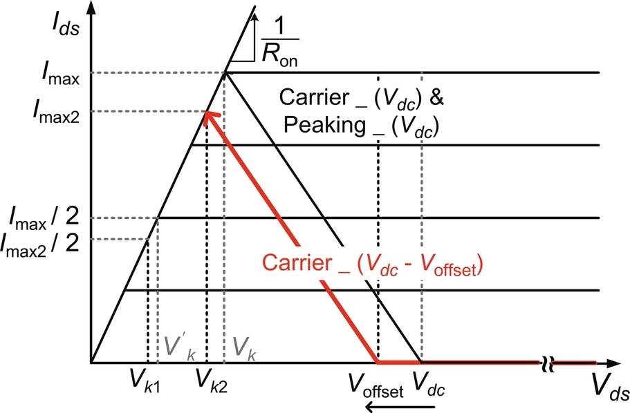
The symbols are defined in the figure. The knee voltages at the first peak efficiency point before and after changing the drain bias voltage of the carrier amplifier are assigned to V′k and Vk1, respectively. Imax and Imax2 are the maximum currents for the load lines, respectively. The Voffset is the reduced amount of the drain bias voltage from Vdc due to the knee effect. The fundamental load impedance (ROPT), output power of the carrier amplifier (PBO), and efficiency at the first peak efficiency region (ηBO) can be derived as


Fig. 3.2 presents the load line of the carrier and peaking amplifiers at the peak output power, where both amplifiers generate their full power. The fundamental load impedance, output power, and efficiency of the carrier amplifier at the region can be derived as


With the similar calculation for the peaking amplifier, the overall output power and the efficiency of the Doherty amplifier at the peak power can be represented by following equations:


Thus, the output back-off level in dB, Pback-off (dB), can be obtained from Eqs. (3.3), (3.8):
The back-off level in Eq. (3.10) is calculated using MATLAB simulation as a function of Ron and is depicted in Fig. 3.3. The original Vdc of the Doherty amplifier is assumed to be 28 V. Under the load modulation condition from 2ROPT to ROPT, Vdc of the carrier amplifier, which delivers the 6 dB back-off level, is decreased as Ron is increased. If the carrier amplifier is biased at the Vdc, the back-off level is reduced, lower than 6 dB for all Ron. This means that the Doherty amplifier does not reach to the maximum efficiency at the 6 dB back-off output power level but at a higher power level. Therefore, the peaking amplifier should be turned on at the higher output power level in order to have the maximum efficiency at the first peak point. In this operation, since the peaking amplifier is turned on at the higher output power level, the load of the carrier amplifier cannot be modulated properly, and the carrier amplifier gets into the saturated region. However, this simulation result shows that with the reduced carrier amplifier's Vdc, the peak efficiency can be achieved at the 6 dB back-off level. This curve also shows that, with the further reduced drain bias of the carrier amplifier, the back-off power point can be adjusted to a lower power region if it is needed to amplify the signal with a large peak-to-average power (PAPR).

Fig. 3.4A shows the efficiencies of the Doherty amplifier at the back-off output power (BO) and peak output power (PEP) level when the 6 dB back-off level is maintained by reducing the drain bias voltage of the carrier amplifier. As the Ron is increased, the fundamental output voltage swing is reduced, and the efficiencies at both output power levels are decreased. Because the knee voltage is increased from Vk1 to Vk2 due to the load modulation, the efficiency at the peak output power is lower than that at the back-off output power level. Fig. 3.4B shows the output power degradation when the 6 dB back-off level is maintained. Because the Vdc of the carrier amplifier is decreased further with a larger Ron, the fundamental output current and voltage of the carrier amplifier are further reduced, resulting in the output power degradation. However, the output power degradation at the peak output power is smaller than that at the back-off output power level due to the peaking amplifier power generation with Vdc.

Based on the analysis, a Doherty amplifier has been designed using GaN HEMT device. The Vdc of the peaking amplifier is 28 V and that of the carrier amplifier is reduced to 22.4 V-based Ron of 0.65 Ω in Fig. 3.3. Fig. 3.5A and B shows the efficiencies of the conventional Doherty and the modified Doherty amplifier. By reducing the Vdc of the carrier amplifier to 22.4 V, the maximum efficiency could be achieved accurately at the 6 dB back-off output power level with 3.43% improved drain efficiency, while the peak power is reduced by 0.88 dB. This reduced power is the consequence of the reduced drain bias of the carrier amplifier. Fig. 3.5C presents the gain profiles versus the output power level for each amplifier and overall Doherty amplifier. Because the GaN HEMT device has a low gm at the low Vdc region, the carrier amplifier of the modified Doherty amplifier has relatively low gain compared with the conventional carrier amplifier. On the other hand, the peaking amplifier delivers the same fundamental output power and gain, comparable with the conventional Doherty case. Accordingly, the overall gain flatness versus the output power level of the modified Doherty amplifier is better than the other case. In spite of the lower gain and output power level, the modified Doherty amplifier delivers improved efficiency as shown in Fig. 3.5B.

Fig. 3.6 shows the simulated load impedances and the fundamental drain currents of the carrier and peaking amplifiers versus the output power level, respectively. When the peaking amplifiers of both the Doherty amplifiers are turned on at the 6 dB back-off output power level as shown in Fig. 3.6B, the modified Doherty amplifier converges properly to the 50 Ω load impedance, delivering the proper load modulation, while the conventional one does not.

In summary, the modified Doherty amplifier employing asymmetrical Vdc is a very useful technique for the proper load modulation with first peak efficiency at the 6 dB back-off point and the flatter gain versus the output power level. However, to take the advantages, the peak power is reduced because of the lower drain bias of the carrier amplifier. Therefore, the Doherty amplifier using the optimized offset lines, which has a larger load modulation ratio, may be a preferred technique than the modified Doherty amplifier described in this section. This asymmetrical drain bias technique can be employed to optimize the first peak efficiency point of a Doherty amplifier. The possibility is shown in Fig. 3.3.
3.2 Optimized Design of GaN HEMT Doherty Power Amplifier With High Gain and High Efficiency
Theoretically, the gain of a carrier amplifier having 2ROPT should be 3 dB higher than that with ROPT. However, the nonlinear input capacitance of the device affects the input match, and the gain can be different according to the operation point. For a proper load modulation with a high gain and high power-added efficiency (PAE), as we describe in the previous section, the input of the carrier amplifier should be matched at the first peak power region with 2ROPT and that of peaking at the peak power region. These optimized design based on the GaN HEMT device is introduced.
3.2.1 Optimized Design of Carrier and Peaking Amplifiers
In a conventional Doherty architecture, the input of the carrier amplifier is conjugate-matched at the peak power with the output load of ROPT. This match produces mismatch at a back-off power level and degrades the gain and the PAE. To solve the problem, the input should be matched at the first peak efficiency point.
Fig. 3.7A shows the nonlinear equivalent circuit model of the GaN HEMT. Here, we assume that the current source sees the load RL for a power match. The extracted input capacitance, Cin, of the model is given by

The Cgs increases as the input power increases. The output load, RL, of the carrier amplifier decreases from 2ROPT to ROPT through the load modulation. As a result, the input capacitance, Cin, of the carrier amplifier is varied as the input power increases as depicted in Fig. 3.7B. This Cin variation affects the power matching and gain.
Fig. 3.8 shows the source-pull simulation results for the fundamental impedance matching points of the carrier amplifier for the output load impedances of ROPT and 2ROPT. The input power level for ROPT is 6 dB higher than that for 2ROPT. As the load impedance is modulated from 2ROPT to ROPT with the increased input power, the effective input capacitance decreases. By matching the input impedance at the first peak power level with the 2ROPT load, the gain of the carrier amplifier at the back-off region can be matched accurately with high efficiency although the matching tolerance is small. The slight mismatch at the lower power region (below the first peak power) provides a flat gain of the Doherty amplifier because the gain at the lower power region is higher than that at the first peak power due to the smaller Cin. The power match at the higher power operation is maintained because the optimum impedance contour at the high power region is insensitive due to the saturated operation with large tolerance as shown in the figure.

In Fig. 3.9, the CW characteristics of the first peak input matched carrier amplifier is compared with the peak power matched conventional amplifier. The new design allows a proper Doherty modulation since the gain difference between the 2ROPT and ROPT matches is about 3 dB. However, the conventional design can achieve the load modulation through the saturated operation of the peaking amplifier only because the two gains are almost identical. This load modulation through the saturated operation is described in Section 5.2.

The input of the peaking amplifier is conjugate-matched at the high power level to maximize the gain at the peak power level. The harmonics of the output impedance for the carrier and peaking amplifiers are matched to the optimum impedances for a high saturated drain efficiency, using LC parallel network circuits. The design method of the saturated amplifier can be found at the further reading. Fig. 3.10 represents the schematic of the proposed Doherty amplifier, which is implemented in MMIC.

3.2.2 Operation of the Optimally Matched Doherty Amplifier
For the simple circuit topology in MMIC, the fundamental output impedance at the output node of the carrier amplifier increases from 50 to 100 Ω, instead of the conventional design of 25 to 50 Ω, and that of the peaking amplifier decreases from infinity to 100 Ω as shown in Fig. 3.11A. For the optimum Doherty operation, the input power driving needs to be an uneven drive. The uneven input dividing is normally realized using the uneven power divider. It can be achieved using the nonlinear input capacitance of the peaking amplifier also as described in Section 5.3.1. Similarly to the nonlinear capacitance case, we could easily realize the uneven input dividing using the input matching. As shown in Fig. 3.11B, 1 dB more power is delivered to the carrier amplifier at the low-power operation and to the peaking amplifier at the high power. Fig. 3.12 shows a CW simulation result of the Doherty amplifier implemented at 1.8 GHz using TriQuint 3MI 0.25 m gallium nitride (GaN) high-electron-mobility transistors (HEMT) MMIC. The DE is more than 52% at the 6 dB back-off power and 59% at the peak power without degradation during the load modulation. Through the optimized input matching for the carrier amplifier, the gain at the back-off power is high for the single stage amplifier, over 19.5 dB. Because of the high gain of the carrier amplifier at the back-off power level, the gate bias voltage for the peaking amplifier can be increased, preventing the gain degradation of the Doherty amplifier at the modulation region as shown in Fig. 3.12.


The implemented integrated circuit size except for the RF choke inductor is 2.28 × 3.09 mm as shown in Fig. 3.13. Drain bias voltage is 28 V for both the carrier and peaking amplifiers, and gate bias voltages are − 2.8 V for the carrier amplifier and − 3.26 V for the peaking amplifier. The Doherty amplifier is tested using an LTE signal with 10 MHz bandwidth and 6.5 dB PAPR at 1.8 GHz. The Doherty amplifier achieves a drain efficiency of 57.2% (PAE of 56.3%) and a gain of 18.8 dB at an average output power of 35.6 dBm.

3.3 Optimized Peaking Amplifier Design for Doherty Amplifier
The peaking amplifier operates at a class C bias and has a lower maximum output power than that of the carrier amplifier. Because of the low output power of the peaking amplifier, the load modulation of the Doherty network cannot be properly carried out. To solve the problem, an inductive second harmonic load is employed at the input to generate the out-phased second harmonic component. The out-phased second harmonic flattens the sign wave, and the conduction angle of the input voltage waveform is enlarged, restoring the decreased conduction angle and the output power. In addition, the peaking amplifier can be turned on at a higher input power due to the reduced peak current, and the first peak efficiency of the Doherty amplifier is enhanced.
3.3.1 Optimized Design of Peaking Amplifier for Proper Doherty Operation
For the proper load modulation of the Doherty amplifier, the output currents of the carrier and peaking amplifiers should be increased with the input voltage as shown in Fig. 3.14. To get the current prolife, as we have discussed earlier, the transconductance of the peaking amplifier should be two times larger than that of the carrier amplifier. To minimize the production cost, however, the device sizes of the carrier and peaking amplifiers are the same since they generate the same maximum power. To overcome the lower power problem, the uneven input drive or the gate bias adaptation technique can be employed.

The problem can be solved by the input second harmonic voltage control, also. Usually, the input second harmonic load of a power amplifier is shorted for a small conduction angle of the output current, which is required for a high-efficiency operation. However, we can utilize the input second harmonic voltage generated from the nonlinear input capacitor to increase the conduction angle and thereby increase the output power. The input capacitance variation for the bias voltage has a reverse characteristic to the output capacitor, that is, it increases as the gate-source voltage increases as shown in Fig. 3.15A, and it generates the out-phased second harmonic voltage. In contrast to the in-phased second harmonic voltage, the out-phased second harmonic voltage flattens the peak of the voltage waveform as shown in Fig. 3.15B. With the flattened input voltage waveform, the effective conduction angle increases, compensating the reduced conduction angle of the peaking amplifier due to the class C bias. In addition, the peak value of the input voltage decreases, allowing the peaking amplifier to turn on late at the same gate bias condition. Therefore, the peaking amplifier with the peak flattened input voltage waveform is suitable for the ideal Doherty operation. To take full advantage of the nonlinear input capacitor, the input second harmonic load should be an inductive load. As shown in Fig. 3.15C, the peak input voltage decreases with the properly tuned inductive second harmonic load.

3.3.2 Simulation and Experimental Results
To validate the inductive harmonic tuning concept, a Doherty amplifier is designed at 2.14 GHz using TriQuint 0.25 μm GaN HEMT process. With the inductive input second harmonic load for the peaking amplifier, the input voltage has a peak flattened waveform. Due to the voltage waveform, the conduction angle of the peaking amplifier increases, and the peak input voltage is decreased as shown in Fig. 3.16.

Fig. 3.17 shows the CW performances of the designed carrier and peaking amplifiers. The input second harmonic load of the carrier amplifier is shorted, and the peaking amplifiers are designed with the short and inductive loads. VGS is − 3 V for the carrier amplifier and − 4.5 V for the peaking amplifier. With the second harmonic short, the peaking amplifier delivers a lower output power and a higher efficiency than the carrier amplifier. However, with the inductive input second harmonic load, the peaking amplifier generates a larger output power, comparable with the carrier amplifier. In addition, with the same gate bias condition, the peaking amplifier with the inductive input second harmonic load turns on later than that of the peaking amplifier with the input second harmonic short circuit. These CW characteristics of the peaking amplifier are beneficial for the Doherty amplifier operation. Although the efficiency is degraded a little, the power is more important for the peaking amplifier.

Fig. 3.18 shows the schematic of the Doherty amplifier adopting the second harmonic tuned peaking amplifier. To realize the inductive input second harmonic load, an inductor is added after the second harmonic short circuit at the input of the peaking amplifier. The device size of the peaking amplifier is the same as that of the carrier amplifier. VGS of the peaking amplifier is increased to − 4.3 V to get the same turn-on voltage. Fig. 3.19 shows the two-tone performance of the Doherty amplifier. At the output power of 37 dBm, the IMD3s at the two sides are lower than − 35 dBc, and the power-added efficiency is 47% (including the DC power consumption of the drive stage).


Fig. 3.20 shows the fabricated Doherty amplifier based on the schematic in Fig. 3.18. The integrated circuit size except for the RF choke inductor is 2.3 × 3.5 mm. The drain bias voltages are 28 V for the power stage of the carrier and peaking amplifiers and 20 V for the drive amplifier. The gate bias voltages of the drive amplifier and the carrier amplifier are − 2.8 V and that for the peaking amplifier is − 4.2 V. Fig. 3.21 shows the measured two-tone performance of the fabricated Doherty amplifier, which is similar to the simulation one. Fig. 3.22 shows the performance of the fabricated Doherty amplifier for the LTE signal at 2.14 GHz with a 10 MHz bandwidth and 6.5 dB PAPR. At the output power of 46.7 dBm, ACLR is − 35 dBc, PAE is 46.7% (including the DC power consumption of the drive stage), and gain is 29.3 dB.


In conclusion, the peaking amplifier cannot deliver the same maximum output power as that of the carrier amplifier because of the low gate bias voltage of the peaking amplifier and cannot properly modulate the load like an ideal Doherty amplifier. To solve the problem, the inductive input second harmonic load is employed. With the harmonic load, the input voltage becomes the peak flattened waveform, and it enlarges the conduction angle of the peaking amplifier. Therefore, the reduced conduction angle of the peaking amplifier, due to the low gate bias, is restored, and the proper Doherty operation could be realized.
3.4 Saturated Doherty Amplifier
A Doherty amplifier is based on the carrier amplifier with a deep class AB bias and the peaking amplifier with a class C; thus, the maximum efficiency of 78.5% is expected. However, the efficiency can be even higher by employing a switching amplifier as an unit amplifier but at the expense of linearity. A class F or F− 1 amplifier is a good choice since the harmonic-controlled matching topology could provide higher efficiency. To get the desired efficiency, the fundamental, second, and third harmonic impedances should be properly controlled simultaneously. In this section, a saturated Doherty amplifier design using the class F amplifier topology is introduced to maximize efficiency. But class F− 1, class E, or other switching/saturated amplifiers can be designed similarly.
The unit amplifier should be operated at the saturated mode, and the Doherty amplifier is named as a saturated Doherty amplifier. The fully matched output matching network is discussed in this section, including the harmonic control circuit (HCC) for the saturated operation. The operational behavior of the saturated Doherty amplifier is analyzed with finite harmonic contents, including the harmonic-controlled load modulation behavior, efficiency, and linearity.
3.4.1 Operational Principle of the Saturated Doherty Amplifier
The efficiency of the Doherty amplifier can be enhanced by employing the carrier and peaking amplifiers based on the class F− 1 mode. Fig. 3.23 shows the schematic diagram of the fully matched saturated Doherty amplifier including the HCC and offset lines.

Fig. 3.23A shows an operational diagram of the saturated Doherty amplifier. For the Doherty operation, the carrier amplifier is biased at the pinch off and the peaking amplifier below the pinch off. The current and voltage waveforms at the devices of the carrier and peaking amplifiers are shaped by the harmonic impedances of the HCC. Theoretically, the high efficiency can be achieved in class F operation by generating half-sinusoidal current and square-wave voltage waveforms. These waveforms can be realized by creating the zero impedances at all even harmonics and infinite impedances at all odd harmonics. However, in a practical design, all harmonic contents cannot be controlled. Moreover, the amplifiers do not operate in the saturated mode for all power levels, either. Thus, a HCC, which can control the second and third harmonics, has been employed in front of the output matching circuit since the HCC does not need to be modulated. The Doherty circuit topology is depicted in Fig. 3.24. The HCC, which is shown in Fig. 3.25, shows the open and short circuits for the class F harmonic tuning. The harmonic matching impedances should not be changed with the matching and load modulation circuits. For the purpose, the second and third shorts are introduced after cutting off the impedance modulation effect. For proper Doherty operation, the offset line at the back of the output matching circuit has also been employed. Therefore, the harmonic control circuit is attached right at the drain terminal, and a tuning line is added for compensating the harmonic detuning effect by the devices' output capacitance. The amplifier circuit topology is depicted in Fig. 3.25.


The analysis of the circuit is based on the following assumptions:
- (1) Each current source is linearly proportional to the input voltage above the pinch-off voltage.
- (2) The voltage waveform depends only on the fundamental and third harmonic components.
- (3) The maximally flat voltage waveform is generated by a 1/9 amplitude ratio and 180 phase difference between the fundamental and third harmonic component voltages, which is the voltage waveform of a class F amplifier.
- (4) The fundamental load impedance is properly modulated using the uneven power drive.
Fig. 3.23B represents the magnitudes of the fundamental current and voltage according to the input drive voltage. Since the current and voltage waveforms represent the half-sinusoidal current and maximally flat voltage waveforms, I1,max and V1,max are a half of ipeak and 9/8 of VDC, respectively. Here, I1,max and V1,max are the maximum fundamental components of the current and voltage, respectively; ipeak is the maximum current, and VDC is the dc bias voltage. At the low-power region (0 < Vin < Vturn on), where only the carrier amplifier is active, the fundamental and dc currents of the amplifier are given by


where Idc,c is 1/π of ipeak and Vmax is the maximum input voltage.
To analyze the load modulation behavior of the saturated Doherty amplifier, we use ZT = ROPT and ZL = ROPT/2, in Fig. 3.23A. The load impedance of the carrier amplifier ZC is given by

Due to the maximally flat voltage waveform, the fundamental voltage component is 9/8 times larger impedance than that of the class B amplifier. Thus, the load impedance of each amplifier is designed to have 9/8 times larger impedance than the conventional amplifier.
At the higher power region, both the carrier and peaking amplifiers are active. The amplifier is unevenly driven with the power ratio σ, which is defined in Eq. (2.4):

where


Here, ψ is the turn-on portion, and I1, p is the fundamental component of the peaking current with a conduction angle of θp.
The fundamental and dc currents of the peaking amplifier are expressed as


The load impedances of the carrier and peaking amplifiers are given by


The fundamental load impedance of the carrier amplifier is modulated from 2ROPT to ROPT, and the load impedance of the peaking amplifier modulated from ∞ to ROPT while the second harmonic short and third harmonic open impedances are maintained.
3.4.2 Efficiency and Linearity of the Saturated Doherty Amplifier
The power-level-dependent operation is explored by defining the saturation state and the unsaturation state according to the amplitude ratio/phase difference between the fundamental and third harmonic voltage components. The amplitude ratio α and the relative phase difference β are expressed as


where V1 and V3 are magnitudes of the fundamental and third harmonic voltages, respectively. ϕ1 and ϕ3 are phases of the fundamental and third harmonic voltages, respectively. At the saturation state, the amplifier should generate the half-sinusoidal current and maximally flat voltage waveforms with α = 1/9 and β = 180° at the given drive level. α and β values of the saturated Doherty amplifier have been investigated using the ADS simulator. Based on the data, we have analyzed the efficiency and the linearity.
3.4.2.1 Efficiency of the Saturated Doherty Amplifier
The efficiency analysis can be carried out using only the fundamental and dc components according to the current and voltage waveforms. At the low-power region (0 < Vin < Vturn on) where only the carrier amplifier is turned on, the RF and dc powers are given by


From Eqs. (3.26), (3.27), the efficiency becomes

The carrier amplifier operates at the unsaturated state until the (8/9) Vturn on input drive level. At this level, the amplifier has a class B peak efficiency due to the larger load impedance as shown in Fig. 3.26. The efficiency increases further to that of the third harmonic tuned class F amplifier as the amplifier is pushed into saturation. The peaking amplifier operates similarly. The efficiency of the peaking amplifier is slightly higher with deeper class C operation.

The load lines are slightly elliptical at a low drive level, and the load line of the carrier amplifier reaches to the minimum allowable voltage at the peaking turn-on point, as shown in Fig. 3.27A where the turn-on voltage of the peaking amplifier (Vturn on) is set to Vmax/2. The amplifier reaches to the saturation state above this drive level, and as shown in Fig. 3.26, the efficiency increases from the class B peak efficiency (point A) to the class F peak efficiency (point B). The load line changes from the slightly elliptical to the quasi-“L” curve at the turn-on voltage, as shown in Fig. 3.27A, but the line cannot make the perfect “L” curve because the harmonic voltage control is limited to the third harmonic. This state illustrates that the amplifier has the half-sinusoidal current and maximally flat voltage waveforms, and the efficiency can reach to the peak efficiency of the class F amplifier with third harmonic tuning, i.e., 88%.

At the higher power region (Vturn on < Vin < Vmax), both amplifiers are active. The RF and dc powers are sum of the two amplifiers' and are given by


From Eqs. (3.29), (3.30), the efficiency becomes

where,

Since the load impedances of the both amplifiers decrease, the load lines of the carrier amplifier move up while maintaining the quasi-“L” curves, as shown in Fig. 3.27A, and the carrier amplifier operates in the saturation state. On the other hand, the current and voltage swings of the peaking amplifier increase in proportion to the drive level due to the proper load modulation, but the amplifier maintains the unsaturation state until it reaches to the minimum allowable output voltage level (point C). In this situation, the load lines of the amplifier are slightly elliptical until it reaches to the minimum allowable output voltage level. For the input power higher than that of the point C operation, the load line becomes the quasi-“L” curve, as shown in Fig. 3.27B. The peaking amplifier reaches to the saturation state after it passes the minimum allowable output voltage level, and both amplifiers have the half-sinusoidal current and maximally flat voltage waveforms at the maximum drive level (point D). The efficiency of the saturated Doherty amplifier, which is the average efficiency of the two amplifiers, is higher than the peak efficiency of the carrier amplifier due to the higher efficiency of the class C bias peaking amplifier, as shown in Fig. 3.27. The operation states of the Doherty amplifier are summarized in Table 3.1.
Table 3.1
| Low-Power Region (A) | Medium-Power Level (B) | High-Power Region (C) | High Power Level (D) | |
|---|---|---|---|---|
| Carrier amplifier | Unsaturated state | Saturation state | Saturation state | Saturation state |
| Peaking amplifier | Turn off | Turn on | Unsaturated state | Saturation state |

3.4.2.2 Linearity of the Saturated Doherty Amplifier
The linearity of the saturated Doherty amplifier is worse than that of conventional Doherty amplifier because the carrier and peaking amplifiers are operated as saturated amplifiers to maximize the efficiency. In the low-power region, the linearity of the amplifier is entirely determined by the carrier amplifier like the conventional one. But the saturated amplifier has a poor linearity. Moreover, the carrier amplifier has a larger impedance load than that of the conventional one, and the amplifier reaches to saturation at a lower input drive level. Thus, the linearity is worse than the conventional Doherty amplifiers and is similar to the class F amplifier. However, in the high-power region, the linearity can be improved by the harmonic cancellation between the two amplifiers with appropriate gate biases like a conventional Doherty amplifier. Due to the linearity improvement mechanism, the Doherty amplifier can be more linear than the switching or saturated amplifiers.
Fig. 28A shows IM3 amplitudes of the carrier and peaking amplifiers and their phase difference. As already stated before, the carrier amplifier has relatively poor linearity with the high IM3 in the low-power region. In the high-power region where the carrier and peaking amplifiers are active, through proper gate bias arrangement of the two amplifiers, we can have IM3 amplitudes of both amplifiers are the same and the phase difference is maintained at ~ 180°. The IMD3 of the Doherty amplifier can be reduced by the harmonic cancellation, as shown in Fig. 3.28B. Therefore, the saturated Doherty amplifier can operate as a reasonably linear amplifier with very high efficiency in spite of the saturated operation, while the class F amplifier cannot.

3.4.3 Improved Harmonic Control Circuit for Saturated Amplifier
In the previous session, we have discussed the Doherty amplifier based on the class F amplifier. However, the saturated amplifier with the second harmonic control, which is not the short or open circuit but an inductive load, can provide very high efficiency, with very simple circuit and the Doherty amplifier based on the saturated amplifier is introduced in this section. The detailed operational behavior of the saturated amplifier can be found in Further Reading of this chapter. A conventional way to tune the second harmonic load in the saturated amplifier is to resonate at the second harmonic frequency using a capacitor. This capacitor is located at the end of the drain bias line and tunes the second harmonic impedance in the slightly inductive region from the resonation. Unfortunately, the second harmonic tuning is affected by the fundamental load modulation of the Doherty network, leading to a mismatch. Therefore, a new second harmonic tuning circuit, without being affected by the load modulation, is needed.
For the carrier amplifier, we generally employ RO = 50 Ω to ROPT matching circuit. To get the 2ROPT load, two impedance transformers (50–25 and 25–100 Ω) and the offset line is used as shown in Fig. 3.29A. The impedance transformers have 90° electric length at the fundamental frequency, and the second harmonic matching impedance is not affected by these transformers. Also, the offset line has 50 Ω characteristic impedance. Therefore, the second harmonic matching impedance for the carrier amplifier is not affected by the load modulation circuit. But an offset line is employed at the peaking amplifier also to make an open circuit at the combining node. However, this offset line cannot provide the open impedance at the second harmonic frequency as shown in Fig. 3.29B, inducing the second harmonic impedance mismatch at the carrier amplifier.

To correct the second harmonic impedance mismatch of the carrier amplifier, a correction circuit is needed. The correction circuit should be independent of the fundamental load modulation and easy to utilize with other techniques required to improve the Doherty amplifier performance. With these constraints, the best location to place the correction circuit is on the offset line since the offset line functions only at the fundamental frequency. The second harmonic impedance correction circuit consists of an adjustable line between the two quarter-wave stubs at the fundamental frequency. The two quarter-wave lines form an open circuit at a connection point on the offset line, and the fundamental impedance is not affected by the correction circuit. But the second harmonic impedance can be controlled as shown in Fig. 3.30. Using this second harmonic control circuit, the Doherty amplifier based on the saturated amplifier can be realized.

3.5 Average Power Tracking Operation of Basestation Doherty Amplifier
The Doherty power amplifier installed in the base station is usually designed at one specific output power level. However, the total data usage can vary depending on the time of day. Thus, the output power of the power amplifier needs to be adjusted according to the data usage to reduce the system power consumption. As the average output power is decreased, a normal Doherty amplifier has a lower efficiency. Therefore, the Doherty amplifier needs to be reconfigured properly for the variation of the output power. The simplest solution is an average power tracking (APT) of the Doherty power amplifier through its drain bias voltage control, similar to the APT of a handset power amplifier. The drain and gate bias voltages should be adjusted for the optimized operation at the different output power levels.
In a conventional Doherty amplifier design, it is biased at fixed gate and drain bias voltages as shown in Fig. 3.31A. However, to cover a wide dynamic range of the average output power with high efficiency, the Doherty amplifier needs to be reconfigured for the drain bias adaptation. The efficiency profile through the APT operation is depicted in Fig. 3.31B. As the peak output power is decreased from P1 to P2, the drain bias voltage is reduced to have high efficiency at the low peak power P2. As the peak output power is decreased, the first peak efficiency point is also decreased. The peaking amplifier should be turned on at the lower input power. Therefore, the gate bias voltage of the peaking amplifier should be adjusted accordingly. These behaviors are discussed in the following section.

3.5.1 Derivation of Drain Bias Control Voltage and Output Power
The optimum load lines of an amplifier, which is biased at class B with different drain biases, are shown in Fig. 3.32. When the peak output power P1 is decreased to P2, the optimum drain bias voltage needs to be reduced from Vds,1 to Vds,2, and the knee voltage is moved from Vk1 to Vk2. Therefore, the ratio of P1,linear and P2,linear can be derived as


Because the load impedance is fixed, the ratios of the current and voltage swings are the same for the two power levels and are given by

The knee voltages Vk1 and Vk2 can be described as
and the ratio of Vk1 and Vk2 can be expressed as

By substituting Eq. (3.35) into Eq. (3.33), the optimum drain bias voltage Vds,2 can be derived as

As a result, the drain bias voltages for the carrier and peaking amplifiers should be reduced in proportion to the square root of the peak output power ratio.
3.5.2 Derivation for Gate Bias Control Voltage
As the peak output power is decreased from P1 to P2, the input power should be reduced linearly. Therefore, the peaking amplifier should be turned on at a 6 dB back-off level from the lower input power. To be turned on in the optimum back-off level, the gate bias voltage of the peaking amplifier needs to be increased linearly also. The input power levels, when the peaking amplifier is turned on, can be derived as
where G1 and G2 are gains for P1 and P2 power operations, respectively. However, the lower drain bias operation leads to a lower gain, and the turn-on voltage of the peaking amplifier should be adjusted following Eq. (3.38).
In Fig. 3.33A, the extracted input capacitance, Cin, is shown as a function of the drain bias voltage. As the drain bias voltage is decreased, the input capacitance is increased, and the gain of the carrier amplifier is decreased as shown in Fig. 3.33B. Therefore, the gate voltage of the peaking amplifier should be reduced accordingly. The two mechanisms compensate the variation of the gate bias voltage. As a result, the optimum gate bias voltage of the peaking amplifier is almost the same for the reconfigured Doherty amplifier for the APT operation.

3.5.3 Simulation Result of Reconfigured Doherty Amplifier for APT Operation
To verify the analysis for the bias voltage adaptations of the reconfigured Doherty amplifier, a Doherty amplifier is designed at 1.94 GHz using a Cree GaN HEMT CGH40045 model. The output matching circuits are optimized for efficiency at the drain bias voltage of 30 V. The harmonics are matched to the optimum impedances for an efficient saturated operation as described in the previous section. The simulation is conducted for the peak output powers with 3 dB step. As the peak output power is decreased to 47 and 44 dBm from 50 dBm, the drain bias voltage is reduced to 21.2 and 15 V, respectively. The gate bias voltage of the peaking amplifier is almost the same, slightly increased from − 6 to − 5.5 V for 47 dBm and − 5.3 V for 44 dBm. The simulation results of the reconfigured Doherty amplifier are shown in Fig. 3.34. When the drain bias voltage is 30 V, the efficiencies are around 70% at the peak power (49.5 dBm) and 6 dB back-off level. As the drain bias voltage is reduced to 21.2 V and 15 V, the efficiencies are around 70% and 72%, respectively at the two power levels.

3.5.4 Implementation and Experimental Results
To validate the simulated results of the reconfigured Doherty amplifier for the APT operation, the amplifier is implemented. The Wilkinson power divider is designed for an even power split. The carrier amplifier is set to a deep class AB bias with an idle current of 180 mA. The experiment is conducted with the peak output powers of 50, 47, and 44 dBm, decreased in 3 dB step, and the bias conditions are the same with the simulated ones. The measured results for a CW signal are shown in Fig. 3.35. As the peak output powers are decreased with the 3 dB step, the drain bias voltages are reduced from 30 to 21.2 and 15 V, respectively. The gate bias voltage is remained almost the same, changing from − 6 to − 5.3 V as the drain bias voltage is decreased. As the result, the efficiency and gain characteristics of the reconfigured Doherty amplifier are moved by the 3 dB step as shown in the figure. The Doherty amplifier is tested using a 10 MHz LTE signal with a 6.5 dB PAPR at 1.94 GHz with a 6.5 dB PAPR. As shown in Fig. 3.36, the measured drain efficiencies and gains are 53.2%, 12.8 dB at 42.9 dBm; 54.3%, 11.2 dB at 39.9 dBm; and 53.4%, 9.1 dB at 37 dBm, respectively.

