Chapter 3
Server Chipsets
The story of modern servers is as much the story of specialized chipsets as it is the story of specialized processors and motherboards. The chipset is the motherboard; therefore, any two server boards with the same chipsets are functionally identical unless the vendor has added features to those provided by the chipset or removed support for certain chipset features.
Note
You will sometimes find server motherboards that use the same chipset but differ in their integrated features. Vendors might add additional chips to support additional features, such as a second 10Mbps Ethernet, 100Mbps Fast Ethernet, or 1000Mbps Gigabit Ethernet port. A vendor might also choose not to support some optional features in a given chipset.
Server Chipsets Overview
The chipset typically contains the processor bus interface (called the front-side bus [FSB]), memory controllers, bus controllers, I/O controllers, and more. All the circuits on the motherboard are contained within the chipset. If the CPU is like the engine in your car, the chipset represents the car's chassis. It is the framework in which the engine rests and is its connection to the outside world. The chipset is the frame, suspension, steering, wheels and tires, transmission, driveshaft, differential, and brakes. The chassis in your car is what gets the power to the ground, allowing the vehicle to start, stop, and corner.
In a typical server, the chipset represents the connection between the processor and everything else. In most cases, the processor can't talk to memory modules, adapter boards, devices, and so on without going through the chipset.
Note
The AMD Opteron processors for servers and workstations incorporate memory controllers. Thus, chipsets that support Opteron processors do not contain memory controllers.
Because the chipset controls the interface or connections between the processor and everything else, the chipset ends up dictating which type of processor you have; how fast it will run; how fast each bus will operate; the speed, type, and amount of memory you can use; and more.
In fact, the chipset might be the single most important component in a system, possibly even more important than the processor. Systems with faster processors can be outperformed by systems with slower processors but better chipsets, much like how a car with less power might win a race through better cornering, acceleration, and braking. When deciding on an x86 server, whether it is prebuilt or assembled from parts, it is a good idea to start by choosing the chipset first because the chipset decision dictates the processor, memory, I/O, and expansion capabilities.
Although server chipsets are designed to perform the same types of tasks as desktop chipsets, the feature set included in a typical server chipset emphasizes stability rather than performance, as with a typical desktop chipset. Server-specific chipset features such as support for error-correcting code (ECC) memory, advanced error correction for memory, system management, and a lack of overclocking options demonstrate the emphasis on stability.
Although servers use x86, Itanium, and a variety of RISC processors, this chapter focuses on chipsets used in x86 and Itanium-based servers. There are several reasons for this. When you select an x86 or Itanium processor as the basis for a server, you can typically select from motherboards based on several chipsets that offer different levels of performance and features, either as part of a preconfigured server or as a component of a custom-built server. Many motherboards offer third-party chipsets, which provides additional flexibility in your final selection. However, when you select a server with a RISC processor, the chipset and motherboard are almost always produced by the same vendor that produced the processor. In addition, a single chipset is usually used to support a particular processor model. Product differentiation on a RISC-based server is based far less on the chipset than on factors such as the number of processors, memory size, and form factor.
Server Chipset History
When IBM created the first PC motherboards, it used several discrete (separate) chips to complete the design. Besides the processor and optional math coprocessor, many other components were required to complete the system, with each component requiring its own separate chip.
Table 3.1 lists all the primary chip components used on the original PC/XT and AT motherboards.
Table 3.1 Primary Chip Components on PC/XT and AT Motherboards
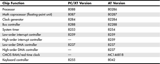
In addition to the processor/coprocessor, a six-chip set was used to implement the primary motherboard circuit in the original PC and XT systems. IBM later upgraded this to a nine-chip design in the AT and later systems, mainly by adding more interrupt and DMA controller chips and the nonvolatile CMOS RAM/real-time clock chip.
All these motherboard chip components came from Intel or an Intel-licensed manufacturer, except the CMOS/clock chip, which came from Motorola. Building a clone or copy of one of these IBM systems required all these chips plus many smaller, discrete logic chips to glue the design together—totaling 100 or more individual chips. This kept the price of a motherboard high and left little room on the board to integrate other functions.
A chipset integrates the functions of two or more discrete chips into a single chip. The first PC chipset was developed by Chips and Technologies, which developed the first PC chipset in 1986.
The Chips and Technologies 82C206 integrated all the functions of the main motherboard chips in an AT-compatible system. This chip included the functions of the 82284 clock generator, 82288 bus controller, 8254 system timer, dual 8259 interrupt controllers, dual 8237 DMA controllers, and even the MC146818 CMOS/clock chip. Besides the processor, virtually all the major chip components on a PC motherboard could now be replaced by a single chip. Four other chips augmented the 82C206, acting as buffers and memory controllers, thus completing virtually the entire motherboard circuit with five total chips. Later, the four chips augmenting the 82C206 were replaced by a new set of only three chips, and the entire set was called the New Enhanced AT (NEAT) CS8221 chipset. This was later followed by the 82C836 Single Chip AT (SCAT) chipset, which finally condensed all the chips in the set down to a single chip.
Intel did not enter the desktop and server chipset business until 1994, which was when the first true server-class processor, the Intel Pentium, was introduced. Although Novell NetWare and other early network operating systems had supported processors from the 8088 through 486 families, those systems did not provide feature support for multiple processors or other hallmarks of modern server design. Starting with the Pentium, chipsets from Intel and other vendors made multiprocessor servers possible.
Although Intel has several other rivals in the desktop chipset business, none of them (VIA Technologies, AcerLabs/ALi, SiS, nVidia, or ATI) are significant rivals to Intel in the manufacture of server chipsets for Intel processors. However, Intel is not alone in supplying server chipsets for its processors. Starting in 1997, ServerWorks (a Broadcom company originally known as Reliance Computer Corporation) introduced its first server chipsets for Intel processors. Today, ServerWorks is the second major supplier of server chipsets for Intel-based servers, with Intel continuing in first place.
Although Advanced Micro Devices (AMD) had made desktop processors for many years, it did not become a significant factor in server chipsets until the development of the Athlon MP processor, its first processor to support SMP operation. AMD now also makes Opteron processors for use in up to four-way servers and produces server chipsets for use with both processor families. Third-party vendors are producing Opteron-compatible chipsets that support up to eight processors.
Sun Microsystems uses two distinct types of architecture in its servers. Its proprietary SPARC-based servers use an equally proprietary motherboard architecture, while its AMD-based Sun Fire X-series and V40z servers use AMD 8000 chipsets.
![]() For more information about Sun servers using the SPARC architecture, see Chapter 19, "Sun Microsystems Servers."
For more information about Sun servers using the SPARC architecture, see Chapter 19, "Sun Microsystems Servers."
Differences Between Server and Desktop Chipsets
Although some chipsets are used for both servers and desktop PCs, and many chipsets are used for both servers and workstations, there are several differences between server and desktop chipsets. Server chipsets generally include the following features not found on desktop chipsets:
- Support for system management software—System management software programs such as IBM Tivoli and CA Unicenter TNG enable a system administrator to determine the condition of a server and take action if memory, processor, or other essential components operate outside normal parameters or fail completely.
- Support for error correction—The ability to detect and correct some types of memory and data errors is an essential feature for any server chipset. Depending on the chipset, error correction might include support for ECC memory, hardware memory scrubbing, chipkill, and ECC support in the North Bridge/South Bridge or hub interface.
Note
Hardware memory scrubbing checks the reliability of the memory subsystem during idle periods and informs the system management software in use of any memory modules that are causing noncorrectable memory errors. Chipkill supports error correction of up to 4 bits per memory module and shuts down memory modules that create too many memory errors while keeping the system operating, using the remainder of the memory modules. Server processors' cache memory often supports ECC as well. For details, see Chapter 2, "Server Microprocessors."
- Support for registered memory—Registered memory, also known as buffered memory, incorporates buffers for greater reliability. However, registered memory is slower than unbuffered memory and is more expensive.
- Support for multiple processors—Although some entry-level servers support only one processor, most servers can be expanded to two or more processors for improved performance.
- Support for 64-bit and 66MHz PCI expansion slots—Most servers feature 66MHz/64-bit PCI expansion slots for use with SCSI and iSCSI drive array host adapters and Gigabit Ethernet network adapters, as well as the more common 33MHz/32-bit PCI slots widely used on desktop computers.
- Support for PCI-X expansion slots—Many recent server chipsets support PCI-X expansion slots as well as PCI expansion slots. The high-performance (up to 133MHz, 64-bit) PCI-X expansion bus is particularly well suited to high-performance SCSI RAID arrays and Gigabit Ethernet adapters, and it is backward compatible with PCI cards. Depending on the server chipset, PCI-X support might be provided by an additional chip in the chipset or might be integrated into the South Bridge (I/O controller hub [ICH]) component of the chipset. PCI-X slots are backward compatible with PCI slots.
- Support for PCI-Express expansion slots—PCI-Express, the newest and fastest member of the PCI family, is supported on some of the newest servers. The exact grouping of lanes per slot varies from chipset to chipset. Typically, servers with PCI-Express support might offer PCI-Express x1 and x4, and some also feature x8 slots. Each PCI-Express lane (x) features a throughput of 250MBps. Thus, a PCI-Express x4 slot has a throughput of 1GBps, which is about the same as that offered by 133MHz, 64-bit PCI-X slots.
Although server chipsets typically have many features not found in desktop chipsets, they also lack some features that are common to most desktop chipsets. For example, audio and advanced video/graphics features are not necessary on servers, and thus it's not surprising that most server chipsets lack support for onboard audio, don't support AGP or PCI-Express video cards, and might not support Microsoft's gaming API, DirectX (which is the case with some ServerWorks chipsets).
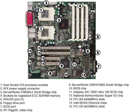
Although server motherboards often support integrated SCSI and PCI or low-end AGP video, these features are not native to a server's chipset but are provided by discrete chips from other vendors. (See Figure 3.1, later in this chapter, for a typical example of a motherboard with onboard SCSI and VGA support.)
Figure 3.1 A typical dual Socket 370 (Pentium III) server motherboard, showing component locations.
The North Bridge and South Bridge Architectures
Most of Intel's earlier chipsets (and, until recently, virtually all non-Intel chipsets) are broken into a multitiered architecture incorporating the North Bridge and South Bridge components, as well as a Super I/O chip:
- North Bridge—North Bridge is so named because it is the connection between the high-speed processor bus (running at speeds from 66MHz to as high as 800MHz in recent designs) and slower buses, such as AGP, PCI, PCI-X, and PCI-Express. The North Bridge is what the chipset is named after, meaning that, for example, what we call the E7505 chipset is derived from the fact that the actual North Bridge chip part number for that set is E7505. Many vendors now use other terms, such as memory controller hub (MCH; Intel) for the North Bridge chip.
- South Bridge—South Bridge was originally named because it is the bridge between the PCI bus (66/33MHz) and the even slower ISA bus (8MHz). On older systems, the PCI bus was used to connect the North and South Bridge chips, but on most recent systems, a dedicated bus such as Intel's Accelerated Hub Architecture or the AMD-developed HyperTransport bus is used for the connection between the North and South Bridge chips. Note that the South Bridge chip is often referred to by other names in recent chipset designs; for example, Intel now uses the term I/O controller hub.
- Super I/O chip—This is a separate chip attached to the ISA bus that is not really considered part of the chipset and often comes from a third party, such as National Semiconductor or Standard MicroSystems Corp. (SMSC). The Super I/O chip contains the logic for legacy ports such as keyboard, PS/2 mouse, serial, and parallel ports, all combined into a single chip. Note that most recent South Bridge chips also include Super I/O functions (such chips are known as Super-South Bridge chips), so most recent motherboards no longer include a separate Super I/O chip.
Figure 3.1 shows a typical dual Socket 370 motherboard using North Bridge/South Bridge architecture, the ServerWorks Super P3TDL3, with the locations of all major chips and components identified.
The North Bridge is sometimes referred to as the PAC (PCI/AGP controller). It is essentially the main component of the motherboard and is the only motherboard circuit besides the processor that normally runs at full motherboard (processor bus) speed. Most modern chipsets use a single-chip North Bridge; however, some of the older chipsets actually consist of up to three individual chips to make up the complete North Bridge circuit.
The South Bridge is the lower-speed component in the chipset and has always been a single individual chip. The South Bridge is a somewhat interchangeable component in that different North Bridge chips are often designed to use the same South Bridge component. This modular design of the chipset allows for lower cost and greater flexibility for motherboard manufacturers. Similarly, many vendors produce several versions of pin-compatible South Bridge chips with different features to enable more flexible and lower-cost manufacturing and design. The South Bridge connects to the 33MHz PCI bus and contains the interface or bridge to the 8MHz ISA bus (if present). It also typically contains dual ATA/IDE hard disk controller interfaces, one or more USB interfaces, and, in later designs, even the CMOS RAM and real-time clock functions. In older designs, the South Bridge contained all the components that make up the ISA bus, including the interrupt and DMA controllers.
The third motherboard component, the Super I/O chip, is connected to the 8MHz ISA bus or the low-pin-count (LPC) bus and contains all the legacy ports that are built in to a motherboard. For example, most Super I/O chips contain the serial ports, parallel port, floppy controller, and keyboard/mouse interface. Optionally, they might contain the CMOS RAM/clock, IDE controllers, and game port interface as well. Systems that integrate IEEE 1394 and SCSI ports use separate chips for these port types, as in Figure 3.1.
Most recent motherboards that use North Bridge/South Bridge chipset designs incorporate a Super-South Bridge, which incorporates the South Bridge and Super I/O functions into a single chip. Additional features, such as the onboard SCSI and VGA video found on the motherboard shown in Figure 3.1, are provided by third-party chips. Although SCSI chips used on server motherboards usually support high-performance SCSI (Ultra160 or Ultra320) and might also support SCSI RAID arrays, VGA video support is usually at a minimal level. For example, the ATI Rage XL video chip used in the motherboard shown in Figure 3.1 supports only 8MB of video memory and lacks advanced 3D graphics performance. Because a server's video is typically used only for monitoring and diagnostics, advanced features are not needed.
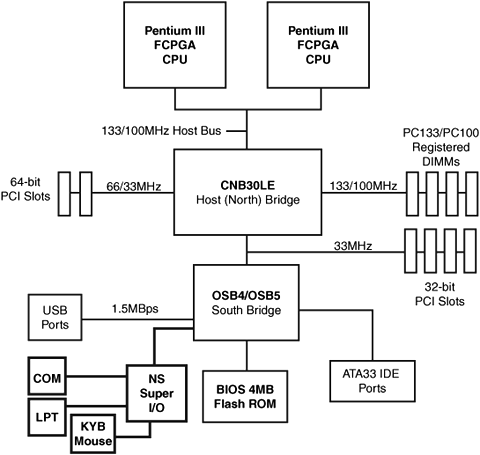
Figure 3.2 illustrates the block diagram of the motherboard shown in Figure 3.1. Note that the 33MHz 32-bit PCI bus is used as the connection between North and South Bridge chips as well as for expansion slots. Also, USB 1.1 ports on this system are used only for low-speed (1.5MBps) input devices, such as keyboards and mouse devices.
Figure 3.2 The North Bridge/South Bridge architecture used by the motherboard shown in Figure 3.1.
Intel Hub Architecture
The newer 8xx, 9xx, 72xx, 73xx, 85xx, and the E75xx series server chipsets from Intel use hub architectures in which the former North Bridge chip is now called a MCH and the former South Bridge is called an ICH. Rather than being connected through the PCI bus, as in a standard North Bridge/South Bridge design, they are connected via a dedicated hub interface that is much faster than PCI.
Hub architectures offer a couple advantages over traditional North Bridge/South Bridge designs:
- Much greater speed—266MBps up to 2GBps (based on version), compared to 133MBps PCI bus.
- Reduced PCI loading—The hub interface is independent of PCI and doesn't share or steal PCI bus bandwidth for chipset or Super I/O traffic. This improves performance of all other PCI bus–connected devices because the PCI bus is not involved in those transactions.
The MCH interfaces between the high-speed processor bus (1066/800/533/400MHz) and video buses such as AGP (up to 533MHz) or PCI-Express x8 (2GBps) or x16 (4GBps), if present. Some systems connect a PCI-X hub (133MHz) to the PCI-Express x8 bus. The ICH interfaces between the ATA (IDE) ports (66/100MHz), the SATA ports (150MBps or faster), and the PCI bus (33MHz). If PCI-Express x1 slots (250MBps) are present, they are usually interfaced via the ICH. Some systems also connect PCI-X slots (100/133MHz) to the ICH.
The ICH also includes an LPC bus, consisting basically of a stripped 4-bit-wide version of PCI designed primarily to support the motherboard ROM BIOS and Super I/O chips. By using the same 4 signals for data, address, and command functions, only 9 other signals are necessary to implement the bus, for a total of only 13 signals. This dramatically reduces the number of traces connecting the ROM BIOS chip and Super I/O chips in a system as compared to the 98 ISA bus signals necessary for older North Bridge/South Bridge chipsets that used ISA as the interface to those devices. The LPC bus has a maximum bandwidth of 16.67MBps, which is much faster than ISA and more than enough to support devices such as ROM BIOS and Super I/O chips.
Intel server chipsets for Pentium 4, Xeon, and Itanium use two different versions of hub architecture:
- Hub Interface 1.5 (HI 1.5)
- Direct Media Interface (DMI or HI 2.0)
HI 1.5 supports a 266MBps connection between the MCH and ICH chips, while DMI supports a 1MBps connection in each direction. HI 1.5 is an updated version of Intel's original Accelerated Hub Architecture (AHA) that was introduced with its first 8xx-series chipsets for Pentium III processors.
Table 3.2 cross-references the hub architectures and Intel server chipsets that use a particular hub architecture.
Table 3.2 Intel Server Chipsets and Hub Architectures
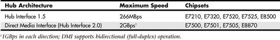
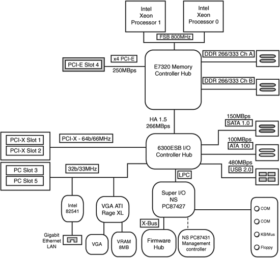
Figure 3.3 shows a typical Intel server motherboard that uses hub architecture—the SE7320SP2.
Figure 3.3 A typical dual Socket 6040 (Xeon) server motherboard, showing component locations.
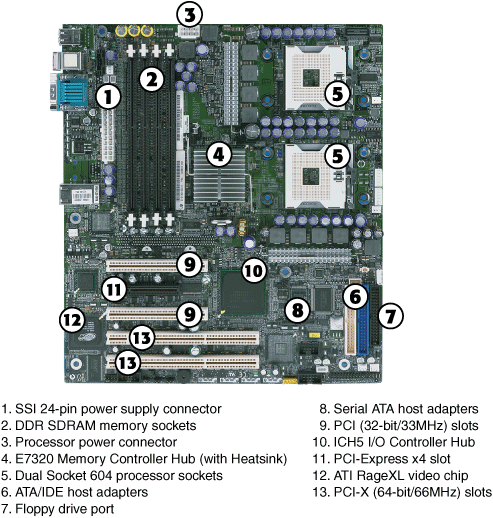
Figure 3.4 illustrates the block diagram of the motherboard shown in Figure 3.4. When you compare this to Figure 3.2, note that the PCI and PCI-X buses are connected to the ICH.
Figure 3.4 The hub architecture used by the motherboard shown in Figure 3.3.
VIA V-Link
V-Link is bus technology that VIA Technologies created to compete with Intel's Hub Architecture. VIA Technologies designed the V-Link architecture to connect its North Bridge and South Bridge chips at speeds matching or exceeding those of Intel Hub Architecture, using a dedicated 8-bit data bus. It is currently implemented in three versions:
- 4x V-Link—4x V-Link transfers data at 266MBps (4x6MHz), which is twice the speed of PCI and matches the speed of Intel's HI 1.5 hub architectures. 4x V-Link was used on the Apollo Pro266, a dual-processor-capable chipset for Intel Pentium III processors.
- 8x V-Link—8x V-Link transfers data at 533MBps (4x133MHz), which is twice the speed of Intel's HI 1.5 hub architecture.
- Ultra V-Link—Ultra V-Link transfers data at 1GBps, which is four times the speed of Intel's HI 1.5 hub architecture and half the speed of Intel's latest DMI hub architecture.
![]() See "VIA Technologies Chipsets for Intel Server Processors," p. 202.
See "VIA Technologies Chipsets for Intel Server Processors," p. 202.
All VIA South Bridge chips in the VT82xx series support V-Link. The first chipsets to use V-Link were VIA's 266-series chipsets for the Pentium III, Pentium 4, and Athlon processor families. VIA's newer chipsets also use V-Link. Although VIA is best known as a desktop and portable chipset vendor, some of its chipsets are used in Athlon-based server motherboards made by various companies.
The ServerWorks Inter Module Bus (IMB)
Most recent ServerWorks chipsets for Intel server processors use a unique high-performance interconnect between the North Bridge and the 64-bit PCI bridge. This interconnect, known as the Inter Module Bus (IMB), is a high-speed serialized data bus. The speed of IMB varies with the chipset, as shown in Table 3.3.
Table 3.3 ServerWorks IMB Performance, by Chipset
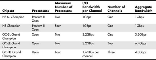
The Champion models' thin IMB performance of 1GBps is sufficient to support Pentium III Xeon processors, which feature 100/133MHz FSB and PC100/133 registered memory. However, the faster performance of Xeon processors, which are based on the Pentium 4 design, demands faster connections. The GC-SL and GC-LE Grand Champion chipsets support Xeon processors with 400MHz or 533MHz FSB connections. The GC-LE's greater memory bandwidth is preferable for use with systems that use multiple 64-bit PCI cards. The GC-HE Grand Champion supports up to four processors, compared to up to two for other Grand Champion models. However, because these processors have FSB speeds of only 400MHz, 4.8GBps of memory bandwidth is adequate to support their operation.
![]() See "Broadcom ServerWorks Chipsets for Intel Processors," p. 196.
See "Broadcom ServerWorks Chipsets for Intel Processors," p. 196.
HyperTransport
AMD's Opteron and other 64-bit AMD processors (Athlon 64, Athlon 64 X2, Turion, and Socket 754 Sempron) use HyperTransport as their interconnection between the processor and the chipset. HyperTransport is also used by most chipsets for these processors as the interconnect between chipset components.
Although HyperTransport is sometimes referred to as "AMD HyperTransport," its original developer, AMD, released HyperTransport to the HyperTransport Consortium (www.hypertransport.org) in 2001. Besides AMD, other founding members include Sun Microsystems, Apple Computer, Broadcom (the parent company of ServerWorks), Cisco Systems, NVIDIA, and Transmeta. The consortium now manages and develops HyperTransport interface technology for use in server and PC chipsets, processors, and other technologies.
How HyperTransport Works
HyperTransport uses low-voltage differential signaling (LVDS) over high-speed connections of varying widths to perform low-latency transfers. HyperTransport is a full-duplex interconnect technology, supporting simultaneous two-way connections between chips. HyperTransport supports asymmetrical connections to provide appropriate bandwidth for different applications. For example, an Opteron processor uses a 16-bit-wide Side A HyperTransport connection to a HyperTransport bridge chip that supports PCI, PCI-X, or PCI-Express connections. However, the bridge chip might use an 8-bit-wide Side B HyperTransport connection to the HyperTransport hub that supports USB and other slower ports.
Note
Connections to the host are known as Side A connections. Connections to the next chip in the chipset are known as Side B connections. HyperTransport speeds are rated in megatransfers (MT) per second.
Tunnels, Bridges, and Hubs
Chips used between the host (processor) and the hub (equivalent to South Bridge) are known as tunnel chips because they pass HyperTransport signals through to the next device. A tunnel chip can provide a direct connection to a device, such as the AMD-8151 AGP 3.0 graphics tunnel, or it can provide bridges (interconnects) to bus types such as PCI, PCI-X, and PCI-Express. HyperTransport devices use independent data streams to carry traffic between the host, tunnel chips, and the hub. When a chip receives a data stream, it determines whether it is the intended target; if it is not, it passes the data stream to the next chip.
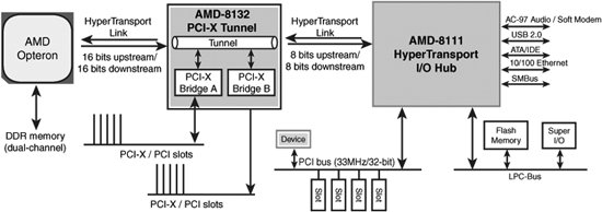
Figure 3.5 shows the block diagram for a typical server configuration using components of the AMD-8000 chipset. Note that the AMD-8000 does not include a North Bridge. That is because the AMD Opteron processor contains its own memory controller rather than relying on a memory controller in the chipset.
Figure 3.5 A typical implementation of HyperTransport on a server using an AMD Opteron processor.
Four-Way and Eight-Way Server Chipsets
Although chipsets designed for single-processor and dual-processor servers are similar in many ways to desktop chipsets, the greater complexity of four-way and eight-way servers that use Intel processors requires the use of more specialized chips than the multipurpose North Bridge/South Bridge or MCH and ICH designs used for single-processor or two-way servers.
A chipset designed for a four-way or eight-way server typically uses several chips to interface and control memory instead of a traditional North Bridge, and it might use specialized chips to provide PCI expansion slot support instead of or along with a traditional South Bridge.
![]() See "The Intel 450NX Chipset," p. 173.
See "The Intel 450NX Chipset," p. 173.
![]() See "The Intel (Corollary) Profusion Chipset," p. 175.
See "The Intel (Corollary) Profusion Chipset," p. 175.
![]() See "Broadcom ServerWorks Chipsets for Intel Processors," p. 196.
See "Broadcom ServerWorks Chipsets for Intel Processors," p. 196.
![]() See "IBM Chipsets for Intel Server-Class Processors," p. 204.
See "IBM Chipsets for Intel Server-Class Processors," p. 204.
![]() See "Hewlett-Packard Server Chipsets for Intel Processors," p. 210.
See "Hewlett-Packard Server Chipsets for Intel Processors," p. 210.
Criteria for Real-World Server Chipsets
Let's examine the leading chipsets used in servers, starting with those used in Pentium Pro–based servers and working all the way through to the latest Xeon, Itanium, Athlon MP, and Opteron chipsets.
In the following sections, the chipsets discussed in detail meet the following real-world server criteria:
- Chipsets that are designed for processors other than the Pentium 4, Pentium D, and Pentium Extreme Edition (which do not support symmetric multiprocessing [SMP]) must support SMP (two or more processors).
- All chipsets, at least, support parity-checked memory or, preferably, ECC memory. Although some vendors sell server motherboards or systems that use chipsets that lack parity or ECC support, you can't consider such systems to be true servers. Because a server is called on to provide mission-critical information to the organization, you need to use technology in your server that ensures that data is reliable.
- Both server and workstation chipsets are discussed because many so-called workstation chipsets are also used in entry-level server installations.
This is the simplest way to summarize what makes a server chipset: If it acts like a server chipset and has been (or can be) used as a server chipset by Intel or a third-party motherboard or system vendor, it is a server chipset.
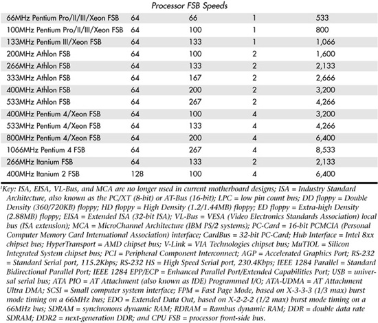
Comparison of System and Component Bus Speeds
The system chipset is the conductor that controls the orchestra of system components, enabling each to have its turn on its respective bus. Table 3.4 shows the widths, speeds, data cycles, and overall bandwidth of virtually all PC buses.
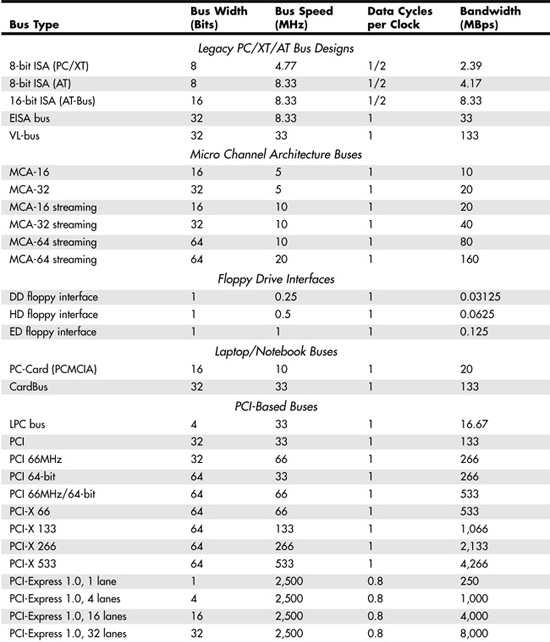
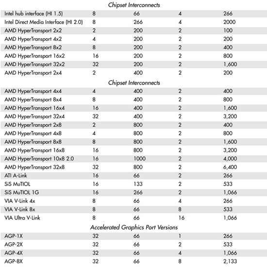
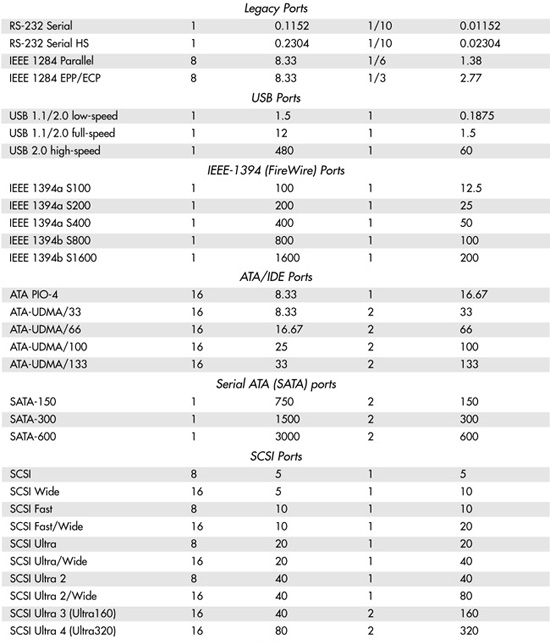
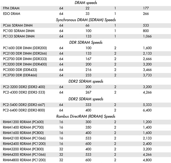
Note that many of the buses use multiple data cycles (transfers) per clock cycle to achieve greater performance. Therefore, the data transfer rate is higher than it would seem for a given clock rate, which provides an easy way to make an existing bus go faster in a backward-compatible way.
The Processor Bus
The processor bus (also called the FSB) is the communication pathway between the CPU and the motherboard chipset (specifically, the North Bridge or MCH). This bus runs at the full motherboard speed—typically between 200MHz and 800MHz in modern systems, depending on the particular board and chipset design.
Most recent one- or two-way servers use bus designs similar to those shown in Figures 3.5 and 3.6. Figure 3.6 shows the bus design for a typical dual-processor Intel Xeon server running at 800MHz CPU (FSB) using the E7525 chipset.
Figure 3.6 A typical bus design for a recent two-way server based on the Intel Xeon processor.
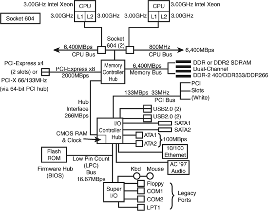
A system running an AMD Opteron processor has a different bus design from the one shown in Figure 3.6:
- The Opteron uses an integrated dual-channel DDR memory controller rather than the traditional North Bridge/MCP design shown in Figure 3.6.
- The Opteron uses three HyperTransport tunnels to carry traffic between the processor and the chipset. Compare Figures 3.5 and 3.6 to get a better sense of these differences.
Because the purpose of the processor bus is to get information to and from the CPU at the fastest possible speed, this bus typically operates at faster than any other bus in the system. The bus consists of electrical circuits for data, addresses (the address bus, which is discussed in the following section), and control purposes. Most processors since the original Pentium have a 64-bit data bus, so they transfer 64 bits (8 bytes) at a time over the CPU bus.
The processor bus operates at the same base clock rate as the CPU does externally. This can be misleading because most CPUs these days run at a higher clock rate internally than they do externally. For example, an AMD Athlon 64 3800+ system has a processor that runs at 2.4GHz internally but only 400MHz externally, whereas a Pentium 4 3.4GHz runs at 3.4GHz internally but only 800MHz externally. In newer systems, the actual processor speed is some multiple (2x, 2.5x, 3x, and higher) of the processor bus.
The processor (FSB) speeds are largely governed by the speed of memory. While memory speeds have increased since the first x86 PCs were introduced 25 years ago, internal processor speeds have gone up by a much higher rate.
![]() See "x86 Processor Speed Ratings," p. 55.
See "x86 Processor Speed Ratings," p. 55.
![]() See "Memory Types Overview," p. 359.
See "Memory Types Overview," p. 359.
The processor bus is tied to the external processor pin connections and can transfer 1 bit of data per data line every cycle. Most modern processors transfer 64 bits (8 bytes) of data at a time.
To determine the transfer rate for the processor bus, you multiply the data bus width (64 bits or 8 bytes for a Pentium III/4 or Xeon or Athlon MP/Athlon 64) by the clock speed of the bus (the same as the base or unmultiplied clock speed of the CPU). For example, if you are using a Xeon 3.6GHz processor that runs on an 800MHz processor bus, you have a maximum instantaneous transfer rate of roughly 6400MBps. You get this result by using the following formula:
800MHz x 8 bytes (64 bits) = 6400MBps
With slower versions of the Xeon, you get either this:
533.33MHz x 8 bytes (64 bits) = 4266MBps
or this:
400MHz x 8 bytes (64 bits) = 3200MBps
With Socket A (Athlon MP), you get this:
333.33MHz x 8 bytes (64 bits) = 2667MBps
or this:
266.66MHz x 8 bytes (64 bits) = 2133MBps
or this:
200MHz x 8 bytes (64 bits) = 1600MBps
With Slot 2 (Pentium III Xeon), you get this:
133.33MHz x 8 bytes (64 bits) = 1066MBps
or this:
100MHz x 8 bytes (64 bits) = 800MBps
This transfer rate, often called the bandwidth, of the processor bus represents the maximum speed at which data can move. Refer to Table 3.4 for a more complete list of various processor bus bandwidths.
The Memory Bus
The memory bus is used to transfer information between the CPU and main memory—the RAM in the system. This bus is connected to the motherboard chipset North Bridge or MCH chip in most server designs. (AMD Opteron processors incorporate the memory controller.) Depending on the type of memory the chipset (and therefore motherboard) is designed to handle, the North Bridge runs the memory bus at various speeds. The best solution is if the memory bus runs at the same speed as the processor bus. Systems that use PC133 SDRAM have a memory bandwidth of 1066MBps, which is the same as the 133MHz CPU bus. Pentium 4 or Xeon systems with the 533MHz bus run dual-channel DDR PC2100 or PC2700 modules, which match or exceed the throughput of the 4266MBps processor bus.
Running memory at the same speed as the processor bus means you don't need to have cache memory on the motherboard.
Note
The main memory bus must transfer data in the same width as the processor bus. This defines the size of what is called a bank of memory, at least when dealing with anything except RDRAM. Memory banks and their widths relative to processor buses are discussed in the section "Memory Banks" in Chapter 5, "Memory."
The SCSI Bus
Although hardly any PCs have integrated SCSI ports, many servers have one or more integrated SCSI ports. SCSI (pronounced "scuzzy") is a general-purpose interface with its roots in SASI (Shugart Associates System Interface). SCSI is a popular interface for attaching high-speed disk drives, RAID arrays, and tape drives to high-end network servers. SCSI is a bus that supports as many as 7 or 15 total devices. Multichannel adapters exist that can support up to 7 or 15 devices per channel.
For more information about SCSI devices and configuration, see Chapter 7, "The SCSI Bus."
About Intel Chipsets
You can't talk about server chipsets today without discussing Intel because the company currently owns the vast majority of the Intel server processor chipset market. It is interesting to note that we probably have Compaq (now part of Hewlett-Packard) to thank for forcing Intel into the chipset business in the first place!
The event that really started it all was the introduction of the EISA bus that Compaq designed in 1989. At that time, Compaq had shared the EISA bus with other manufacturers in an attempt to make it a market standard. However, Compaq refused to share its EISA bus chipset—a set of custom chips necessary to implement this bus on a motherboard.
Intel decided to fill the chipset void for the rest of the PC manufacturers wanting to build EISA bus motherboards. As is well known today, the EISA bus only found short-term market support as part of a niche server business in the early 1990s, but ultimately it failed to become a market success. This opened the door for Intel, which now had a taste of the chipset business that it apparently wouldn't forget.
With the introduction of the 286 and 386 processors, Intel became impatient with how long it took the other chipset companies to create chipsets around its new processor designs; this delayed the introduction of motherboards that supported the new processors. For example, it took more than two years after the 286 processor was introduced for the first 286 motherboards to appear and just over a year after the 386 had been introduced for the first 386 motherboards to appear. Intel couldn't sell its processors in volume until other manufacturers made motherboards that would support them, so it thought that by developing motherboard chipsets for a new processor in parallel with the new processor, it could jumpstart the motherboard business by providing ready-made chipsets for the motherboard manufacturers to use.
After introducing the 420 series chipsets along with its 486 processor in April 1989, Intel realized it controlled over 90% of the components on a typical motherboard because it made both processors and chipsets. What better way to ensure that motherboards were available for its Pentium processor when it was introduced than by making its own motherboards as well and having these boards ready on the new processor's introduction date?
When the first Pentium processor debuted in 1993, Intel also debuted the 430LX chipset, as well as a fully finished motherboard. Now, besides the chipset companies being upset, the motherboard companies weren't too happy, either. Intel was not only the major supplier of parts needed to build finished boards (processors and chipsets) but was now building and selling the finished boards as well. By 1994, Intel dominated the processor and chipset markets for desktop PCs. By the late 1990s, through a combination of internally developed chipsets and shrewd acquisitions, such as Intel's purchase of Corollary, the original developer of Intel's Profusion 8-way chipset, Intel also dominated the processor and chipset markets for entry-level dual and four-way servers.
Now as Intel develops new processors, it develops chipsets and motherboards simultaneously, which means they can be announced and shipped in unison. This eliminates the delay between introducing new processors and waiting for motherboards and systems capable of using them, which was common in the industry's early days.
Starting with the 486 in 1989, Intel began a pattern of numbering its chipsets as shown in Table 3.5.
Table 3.5 Intel Chipset Model Numbers
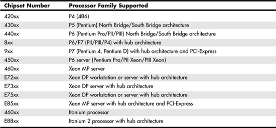
The chipset numbers listed in Table 3.5 are abbreviations of the actual chipset numbers stamped on the individual chips. For example, the 945G chipset supports the Pentium D and Pentium 4 and consists of two main parts: the 82945G Graphics MCH (GMCH, which replaces the North Bridge and includes integrated video) and an 82801GR ICH (ICH7R, which replaces the South Bridge).
Tip
In many cases, the North Bridge/GMCH/MCH chip on recent motherboards is covered up with a passive or active heatsink, and some motherboards also use a heatsink on the South Bridge or ICH chip. To determine the chipset used in these systems, you can watch for motherboard information some systems display at startup. Alternatively, you can use a third-party hardware reporting program such as SiSoftware Sandra (www.sisoftware.co.uk).
Intel Pentium Pro/II/III Chipsets for Servers
Intel was the leading vendor of chipsets for its P6 processor families, which included the Pentium Pro, Pentium II, and Pentium III. Table 3.6 shows the Intel chipsets used on Pentium Pro motherboards. All the chipsets shown in Table 3.6 were designed to be suitable for use in server applications. However, most systems using these chipsets have been retired.
Table 3.6 Intel Pentium Pro Motherboard Chipsets (North Bridge)1
Note
PCI 2.1 supports concurrent PCI operations.
Intel Pentium II/III chipsets that were suitable for use in servers are shown in Tables 3.7 and 3.8. 4xx series chipsets incorporate a North Bridge/South Bridge architecture (Table 3.7), whereas 8xx series chipsets support the newer and faster hub architecture. P6/P7 (Pentium III, Pentium 4, and Xeon) processor chipsets using hub architecture are shown in Table 3.8.
Table 3.7 P6 Processor Chipsets Using North Bridge/South Bridge Architecture
Table 3.8 P6 (Pentium III) Server Processor Chipsets Using Hub Architecture1
Note
Pentium Pro, Celeron, and Pentium II/III CPUs have their secondary caches integrated into the CPU package. Therefore, cache characteristics for these machines are not dependent on the chipset but on the processor instead.
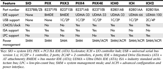
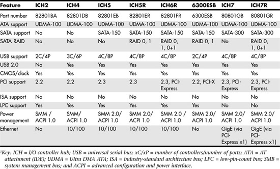
Most recent Intel chipsets for single-processor or dual-processor servers are designed as two-part systems, using a North Bridge (MCH or GMCH in hub-based designs) and a South Bridge (ICH in hub-based designs) component. Often the same South Bridge or ICH component can be used with several different North Bridge (MCH or GMCH) chipsets. Table 3.9 shows a list of all the Intel South Bridge components used with P6-class processors and their capabilities. The ICH2 is also used as part of some of the first seventh-generation (Pentium 4) Intel chipsets.
Table 3.9 Intel South Bridge/ICH Chips for P6 Class CPUs1
The following sections examine the server-class chipsets for P6 processors up through the Pentium III.
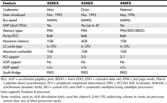
The Intel 450KX/GX (Mars/Orion) Chipsets
The first chipsets to support the Pentium Pro were the 450KX and GX. Although both are commonly known as Orion, the 450KX was originally known as Mars. The 450KX was designed for networked or standalone workstations and is also suitable for low-end servers; the more powerful 450GX was designed for servers. The GX server chipset was particularly suited to the server role because it supports up to four Pentium Pro processors for SMP servers, up to 8GB of four-way interleaved memory with ECC or parity, and two bridged PCI buses. Some vendors, such as ALR, with its Revolution 6x6, designed systems that could use up to six processors using the GX chipset. The 450KX is the low-end server or workstation (standalone user) version of Orion and, as such, it supports fewer processors (one or two) and less memory (1GB) than the GX. The 450GX and 450KX both have full support for ECC memory—a requirement for server and workstation use.
![]() See "Pentium Pro Processors," p. 87.
See "Pentium Pro Processors," p. 87.
The 450GX and 450KX North Bridge comprises four individual chip components: an 82454KX/GX PCI bridge, an 82452KX/GX data path (DP), an 82453KX/GX data controller (DC), and an 82451KX/GX memory interface controller (MIC). Options for QFP or BGA packaging were available on the PCI Bridge and the DP. BGA uses less space on a board.
Note
Quad flat pack (QFA) is a method used for surface-mounting a chip to a board. Chips that use QFA packaging have leads on all four sides of the chip. Ball grid array (BGA) chips use solder balls on the underside of the chip.
The 450's high reliability was obtained through ECC from the Pentium Pro processor data bus to memory. Reliability is also enhanced through parity protection on the processor bus, control bus, and all PCI signals. In addition, single-bit error correction is provided, thereby avoiding server downtime because of spurious memory errors caused by cosmic rays.
![]() See "Parity and ECC," p. 389.
See "Parity and ECC," p. 389.
Until the introduction of the following 440FX chipset, these chipsets were used almost exclusively in fileservers. After the debut of the 440FX, the expensive Mars/Orion chipsets all but disappeared due to their complexity and high cost.
The Intel 440FX (Natoma) Chipset
The first popular mainstream P6 (Pentium Pro or Pentium II) motherboard chipset was the 440FX, which was codenamed Natoma. Intel designed the 440FX to be a lower-cost and somewhat higher-performance replacement for the 450KX workstation chipset. Although the 440FX was designed for use in workstation applications, it was also used as a low-end server chipset by numerous vendors. It offered better memory performance through support of EDO memory, which the prior 450KX lacked.
![]() See "Early Server RAM Types: DRAM, EDO DRAM, and SDRAM," p. 361.
See "Early Server RAM Types: DRAM, EDO DRAM, and SDRAM," p. 361.
The 440FX uses half the number of components that the previous Intel chipset used. It offers additional features, such as support for the PCI 2.1 (concurrent PCI) standard, support for USB 1.1 ports, and reliability through ECC.
The concurrent PCI processing architecture maximizes system performance with simultaneous activity on the CPU, PCI, and ISA buses. Concurrent PCI provides increased bandwidth to better support 2D/3D graphics, video and audio, and processing for host-based applications. ECC memory support delivers improved reliability to business system users.
The main features of this chipset included the following:
- Support for up to 1GB of EDO memory
- Full 1GB cacheability (based on the processor because the L2 cache and tag are in the CPU)
- Support for USB 1.1
- Support for bus master IDE
- Support for full parity/ECC memory
The 440FX consists of a two-chip North Bridge. The main component is the 82441FX PCI bridge and memory controller, along with the 82442FX data bus accelerator for the PCI bus. This chipset uses the PIIX3 82371SB South Bridge chip that supports high-speed bus master DMA IDE interfaces and USB, and it acts as the bridge between the PCI and ISA buses. Figure 3.7 illustrates the design of the 440FX.
Figure 3.7 System block diagram using the Intel 440FX chipset.
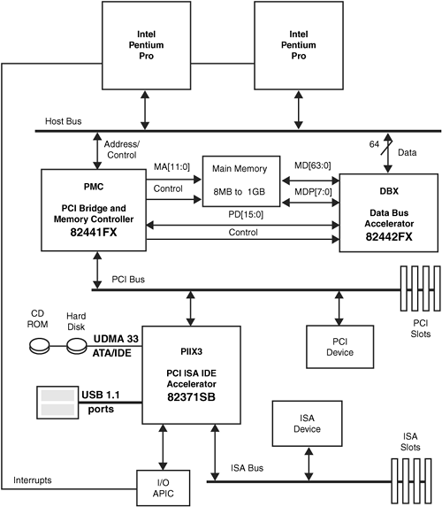
Note that the 440FX was the first P6 chipset to support EDO memory, but it lacked support for the faster SDRAM memory. Also, the PIIX3 South Bridge used with this chipset does not support the faster Ultra DMA IDE hard drives.
The 440FX was the chipset used on the first Pentium II motherboards, which have the same basic architecture as the Pentium Pro. The Pentium II was released several months before the chipset that was supposedly designed for it was ready, so early PII motherboards used the older 440FX chipset. However, this chipset was never designed with the Pentium II in mind, whereas the newer 440LX was optimized specifically to take advantage of the Pentium II architecture. When the 440LX was introduced, the 440FX was quickly superseded.
The Intel 440LX Chipset
The 440LX quickly took over in the marketplace after it was introduced in August 1997. This was the first chipset to really take full advantage of the Pentium II processor. The 440LX chipset was the first Intel Pentium II chipset to use a single-chip North Bridge design, setting a design standard that would be followed by subsequent designs. The 82443LX North Bridge chip incorporated the features that required two chips in its immediate predecessor, the 440BX, and added support for two then-new technologies, AGP video and 66MHz synchronous DRAM (SDRAM). The 440LX's South Bridge, the PIIX4, was also a new design, adding support for Ultra DMA 33 ATA/IDE drives.
![]() See "Pentium II Processors," p. 90.
See "Pentium II Processors," p. 90.
The 440LX chipset's major features included the following:
- Single-chip North Bridge design (82443LX chip)
- Support for the (then-new) AGP video card bus
- Support for 66MHz SDRAM memory
- Support for the Ultra DMA ATA/IDE interface (UDMA/33)
- Support for USB 1.1 ports
The 440LX's design was flexible enough to support all types of Pentium II systems, from two-way servers to desktop computers. It was the most popular chipset for Pentium II systems from late 1997 through spring 1998.
The Intel 440BX Chipset
The Intel 440BX chipset, introduced in April 1998, was the first chipset to run the processor host bus (often called the FSB) at 100MHz. The 440BX was designed specifically to support the faster Pentium II/III processors at 350MHz and higher. The main change from the previous 440LX to the BX is that the 440BX chipset improves performance by increasing the bandwidth of the system bus from 66MHz to 100MHz. Because the chipset can run at either 66MHz or 100MHz, it allows one basic motherboard design to support all Pentium II/III processor speeds based on either the 66MHz or 100MHz processor bus.
Here are the Intel 440BX highlights:
- Support for 100MHz SDRAM (PC100); the now-common PC133 RAM can also be installed, but it will still run at just 100MHz
- Support for both 100MHz and 66MHz system and memory bus designs
- Support for up to 1GB of memory in up to four banks (four DIMMs)
- Support for ECC memory
- Support for ACPI power management
![]() See "Pentium III Processors," p. 93.
See "Pentium III Processors," p. 93.
The Intel 440BX consists of a single North Bridge chip called the 82443BX host bridge/controller, paired with a new 82371EB PCI-ISA/IDE Xcelerator (PIIX4E) South Bridge chip. This South Bridge adds support for the ACPI specification version 1.0 to the features of its predecessor, the PIIX4. Figure 3.8 shows a typical system block diagram using the 440BX.
Figure 3.8 System block diagram using the Intel 440BX chipset.
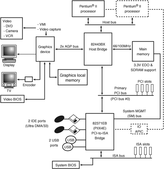
The 440BX was a popular one-way and two-way server chipset during 1998 and into 1999. It offered superior performance and high reliability through the use of ECC, SDRAM, and DIMMs.
The Intel 440GX Chipset
The Intel 440GX AGP set was the first chipset optimized for high-volume midrange workstations and lower-cost servers, and it was Intel's first chipset for the server/workstation version of the Pentium II, the Pentium II Xeon. The 440GX also supports the Pentium III Xeon processor. The 440GX is essentially a version of the 440BX that has been upgraded to support the Slot 2 (also called SC330) processor slot for the Pentium II/III Xeon processor. The 440GX can still be used in Slot 1 designs, as well. It also supports up to 2GB of memory, twice that of the 440BX. Other than these items, the 440GX is essentially the same as the 440BX. Because the 440GX is core compatible with the 440BX, motherboard manufacturers could quickly and easily modify their existing Slot 1 440BX board designs into Slot 1 or 2 440GX designs.
The main features of the 440GX include the following:
- Support for Slot 1 and Slot 2
- Support for 100MHz system bus
- Support for up to 2GB of SDRAM memory
This chipset allows for lower-cost, high-performance workstations and servers using the Slot 2–based Xeon processors.
![]() See "Pentium II Xeon," p. 91.
See "Pentium II Xeon," p. 91.
![]() See "Pentium III Xeon," p. 98.
See "Pentium III Xeon," p. 98.
The Intel 450NX Chipset
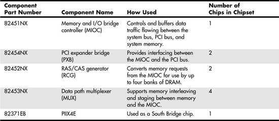
The 450NX chipset (originally known as the 440NX) was designed for multiprocessor systems and standard high-volume servers based on the Pentium II/III Xeon processor. The Intel 450NX chipset consists of four components: the 82454NX PCI expander bridge (PXB), 82451NX memory and I/O bridge controller (MIOC), 82452NX RAS/CAS generator (RCG), and 82453NX data path multiplexer (MUX). As Table 3.10 shows, a full implementation of the 450NX uses two or more of the PXB, RCG, and MUX chips.
Table 3.10 Details of the 450NX Chipset
The 450NX supports up to four Pentium II/III Xeon processors at 100MHz. Two dedicated PCI expander bridges can be connected via the expander bus. Each PXB provides two independent 32-bit, 33MHz PCI buses, with an option to link the two buses into a single 64-bit, 33MHz bus.
Figure 3.9 shows a typical high-end server block diagram using the 450NX chipset.
Figure 3.9 High-end server block diagram using the Intel 450NX chipset.
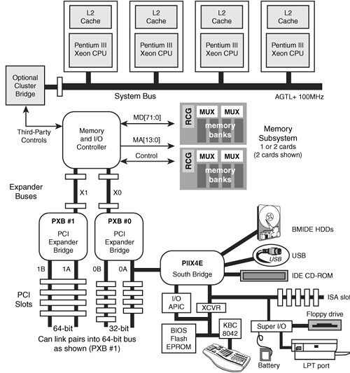
The 450NX supports one or two memory cards. Each card incorporates an RCG chip and two MUX chips, in addition to the memory DIMMs. Up to 8GB of memory is supported in total.
The primary features of the 450NX include the following:
- Slot 2 (SC330) processor bus interface at 100MHz
- Support for up to four-way processing
- Support for two dedicated PCI expander bridges
- Support for up to four 32-bit PCI buses or two 64-bit PCI buses
The 450NX chipset does not support AGP because high-end video is not an issue in network fileservers.
Fujitsu also used the 450NX chipset, to develop its TeamServer M800i series. This eight-way server used two 450NX chipsets linked by Fujitsu's Synfinity interconnect technology and non-uniform memory access (NUMA) memory architecture to create what is, in effect, a tightly coupled computer cluster in a single unit.
![]() See "NUMA Multiprocessing," p. 38.
See "NUMA Multiprocessing," p. 38.
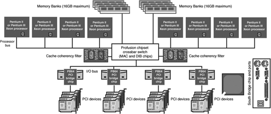
The Intel (Corollary) Profusion Chipset
The Profusion chipset, which supports eight-way Pentium III Xeon servers, is extremely different from most other Intel chipsets for servers. As we have seen, most Intel chipsets for Pentium II/III Xeon servers use some form of the North Bridge/South Bridge chipset architecture originally developed for use with the Intel 486 processor. However, the greater complexity of four-way and larger multiprocessor server architectures using Intel processors requires the use of several specialized chips.
Intel's first chipset to use multiple specialized chips was the 450NX for four-way Pentium II/III Xeon servers (see the section "The Intel 450NX Chipset," earlier in this chapter). Profusion's design, originally developed by Corollary in cooperation with Compaq (now a Hewlett-Packard brand), is even more sophisticated than the 450NX's because of the added challenge of supporting eight processors. Although Corollary began developing the Profusion chipset in 1996, the first systems that used Profusion were not released until late 1999, after Intel purchased Corollary in late 1997, making it a wholly owned subsidiary, and released the chipset to server developers in June 1998.
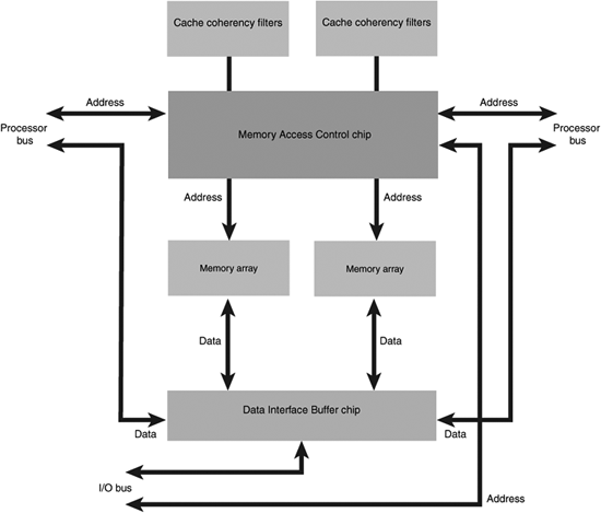
The Profusion chipset creates a five-port (dual memory banks, dual processor buses, and I/O bus) nonblocking crossbar switch using two components:
- One memory access controller (MAC) chip, which also provides a three-way processor bus bridge, support for up to 32GB of SDRAM, and TAG SDRAM management
- One data interface buffer (DIB) chip, which also provides three processor bus data ports with ECC support, two SDRAM data ports with ECC support, and concurrent data transfer on all ports and 64 cache line buffers
These two chips form a five-way crossbar switch that handles data flow between the processors, memory, and I/O bus. The combination of MAC and DIB chips in the Profusion chipset replaces the physical switch often used in other eight-way SMP architectures to interface the processors with memory and I/O bridge connections to system RAM and I/O devices such as PCI slots and PCI/ISA ports. Figure 3.10 illustrates how the MAC and DIB chips work together.
Figure 3.10 The Profusion chipset's MAC and DIB chips form a five-way crossbar switch.
Other components of the Profusion chipset include the following:
- A 64-bit PCI bus bridge chip, the PB64 (also co-developed by Corollary and Compaq), which supports up to 8 66MHz, 64-bit PCI bus masters and up to 16 33MHz, 64-bit PCI bus masters. Up to 4 PB64 chips can be used to provide redundancy and to provide support for mixed PCI speeds. Typically, 1 of the PB64 chips is devoted to 33MHz PCI slots, and the others provide support for 66MHz slots.
- Cache coherency filters (also known as cache accelerators), which are used to improve cache memory performance on eight-way systems; one is required for each four-processor section of an eight-way configuration. A four-way system does not need a cache coherency filter.
- A South Bridge chip (Intel's PXII4E) to provide support for keyboard, mouse, USB, and serial and parallel ports.
The crossbar switch and support for multiple PCI bus bridge chips enable servers based on Profusion to handle memory, processor, cache coherency, and PCI bridge failures while continuing to operate.
Figure 3.11 shows a block diagram of a typical eight-way system based on the Profusion chipset.
Figure 3.11 Block diagram of a typical system based on the Profusion chipset.
From late 1999 through 2001, the Profusion chipset was the leading eight-way server chipset used with Intel server-class processors. Although the Profusion chipset itself has been discontinued, an improved version of the chipset was developed by Compaq (now owned by Hewlett-Packard) for use in servers using the Xeon MP processor. This chipset, the Hewlett-Packard F8, is covered later in this chapter, in the section "The F8 Chipset for Xeon MP."
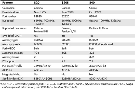
The Intel 820 and 820E Chipsets
The Intel 8xx series chipsets introduced in 1999 represent a major departure from the 4xx-series chipsets previously used by Intel for its one-way and two-way servers. The 4xx-series chipsets used the North Bridge/South Bridge design, which use the 133MBps PCI bus to carry signals between the components. The 8xx-series chipsets replace the North Bridge with an MCH, and the South Bridge with an ICH. Intel 8xx systems replace the PCI bus interconnection between chipset components with a 266MBps dedicated bus known variously as the Accelerated Hub Architecture (AHA) or, in later systems, Hub Architecture 1.5.
![]() See "Intel Hub Architecture," p. 151.
See "Intel Hub Architecture," p. 151.
The Intel 820 chipsets were designed to support Slot 1 or Socket 370 processors, such as the Pentium III and Celeron. The 820 chipset was the first to support RDRAM memory technology, a 133MHz system bus, and 4x AGP.
The 82820 MCH provides the processor, memory, and AGP interfaces. Two versions are available: One supports a single processor (82820), and the other supports two processors (82820DP), making the 820E suitable for use in low-end two-way servers. Either is designed to work with the same 82801 ICH as used with the other 800-series chipsets, such as the 810 and 840. The 820 chipset also uses the 82802 firmware hub (FWH) for BIOS storage and for the Intel random number generator (RNG).
The 820 chipset was designed to use RDRAM memory, which has a maximum throughput of up to 1.6GBps. The 820 supports PC600, PC700, and PC800 RDRAM, delivering up to 1.6GBps of theoretical memory bandwidth in the PC800 version. PC800 RDRAM is a 400MHz bus running double-clocked and transferring 16 bits (2 bytes) at a time (2x400MHzx2 bytes = 1.6GBps). Two RIMM sockets are available to support up to 1GB of total system memory.
The AGP interface in the 820 enables graphics controllers to access main memory at AGP 4x speed, which is about 1GB per second—twice that of previous AGP 2x platforms.
820 chipset features include the following:
- Single- or dual- (820E) processor support
- 100/133MHz processor bus
- Intel 266MBps hub interface
- PC800 RDRAM RIMM memory support
- AGP 4x support
- ATA-100 (820E) or ATA-66 interface
- Intel RNG
- LPC interface
- AC '97 controller
- One (820) or two (820E) USB 1.1 buses with either two or four ports, respectively
The 820 chipset consists of three main components, with a few optional extras. The main component is the 82820 (single-processor) or 82820DP (dual-processor) MCH, which is a 324 BGA chip. That is paired with an 82801 ICH, which is a 241 BGA chip. Finally, it has the 82802 firmware hub (FWH), which is really just a fancy flash ROM BIOS chip. Optionally, there can be an 82380AB PCI-ISA bridge that is used only if the board is equipped with ISA slots.
The newer 820E version uses an updated 82801BA ICH2, which supports ATA-100 and incorporates dual USB controllers with two ports each, for a total of four USB ports. Although the 820E supports dual processors, few, if any, dual-processor 820E motherboards were ever built.
The Intel 840 Chipset
The Intel 840 was a high-end chipset designed for use in high-performance multiprocessor systems using Slot 1, Slot 2 (Xeon processor), or Socket 370 processors. The 840 chipset uses the same hub architecture and modular design as the rest of the 800 family of chipsets, with some additional components that enable more performance. Figure 3.12 shows a photo of the Intel 840 chipset.
Figure 3.12 Intel 840 chipset, showing the 82840 (MCH), 82801 (ICH), 82802 (FWH), 82803 (MRH-R), 82804 (MRH-S), and 82806 (P64H) chips. (Photograph used by permission of Intel Corporation.)
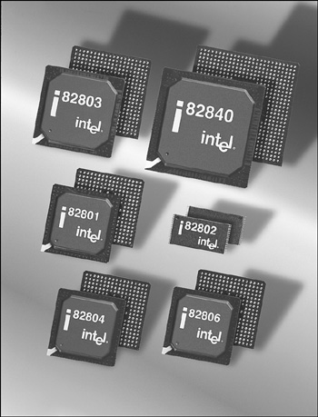
As with the other 800 series chipsets, the 840 has three main components:
- 82840 MCH—This provides graphics support for AGP 2x/4x, dual RDRAM memory channels, and multiple PCI bus segments for high-performance I/O. Equivalent to the North Bridge in older chipset designs.
- 82801 ICH—This is the equivalent to the South Bridge in older chipset designs, except that it connects directly to the MCH component via the high-speed Intel Hub Architecture bus. The ICH supports 32-bit PCI, IDE controllers, and dual USB 1.1 ports.
- 82802 FWH—This is basically an enhanced flash ROM chip that stores system BIOS and video BIOS, as well as an Intel RNG. The RNG provides truly random numbers to enable stronger encryption, digital signing, and security protocols.
In addition to the core components, parts are available for scaling up to a more powerful design. Three additional components shown in Figure 3.12 can be added:
- 82806 64-bit PCI controller hub (P64H)—Supports 64-bit PCI slots at speeds of either 33MHz or 66MHz. The P64H connects directly to the MCH using Intel Hub Architecture, providing a dedicated path for high-performance I/O. This is the first implementation of the 66MHz 66-bit PCI on a PC motherboard chipset, allowing for a PCI bus four times faster than the standard 32-bit 33MHz version.
- 82803 RDRAM-based memory repeater hub (MRH-R)—Converts each memory channel into two memory channels for expanded memory capacity.
- 82804 SDRAM-based memory repeater hub (MRH-S)—Translates the RDRAM protocol into SDRAM-based signals for system memory flexibility. This is used only in 840 systems that support SDRAM.
Figure 3.13 shows the 840 chipset architecture.
Figure 3.13 Intel 840 chipset architecture.
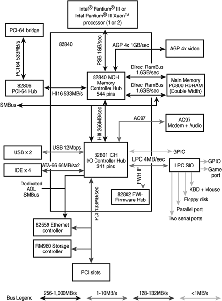
840 chipset features include the following:
- Support for one or two Pentium III or Pentium III Xeon processors
- 100/133MHz processor bus
- Dual RDRAM memory channels, operating simultaneously and providing up to 3.2GBps memory bandwidth (requires 82803 chip)
- 16-bit wide implementation of Intel Hub Architecture (HI16), which enables high-performance concurrent PCI I/O with the optional P64H component
- AGP 4x
- Prefetch cache, unique to the 840 chipset, which enables highly efficient data flow and helps maximize system concurrency
- Intel RNG
- USB 1.1 support
Optionally, network interface and RAID controller interface chips could be added as well. Both Intel and third-party vendors have used the 840 chipset to build dual-processor server motherboards.
Intel Pentium 4 Chipsets for Single-Processor Servers
Although Intel supported .multiple-processor configurations for its Pentium, Pentium II, and Pentium III processors and produced server-class chipsets for all three processor families, its primary multiple-processor (two-way and higher) platforms have been the various members of the Xeon family:
- Pentium II Xeon
- Pentium III Xeon
- Xeon DP (based on the Pentium 4)
- Xeon MP (based on the Pentium 4)
Starting with the Pentium 4, Intel discontinued supporting multiple-processor configurations for its desktop processors. Although Intel continues to support features such as ECC memory and relatively large amounts of RAM (2GB or higher) in some of its Pentium 4 chipsets and sells some entry-level server boards that use the Pentium 4, its primary server platforms are the Xeon (which is based on the Pentium 4 but which uses Socket 603 and Socket 604 and supports up to eight processors in its Xeon MP version) and Itanium family (Intel's first 64-bit processors). If you want to build a multiprocessor server based on Intel processors today, you need to use the Xeon DP, Xeon MP, or Itanium 2 processors. Xeon DP supports up to two-way designs, while Xeon MP and Itanium 2 also support four-way and larger designs.
Tip
If you want the low cost of a single-processor server but want to enjoy virtually all the advantages of two processors in an Intel-based platform, you can select servers based on the dual-core Pentium D or Pentium Extreme Edition processors.
Although some third-party chipsets have been used for entry-level Pentium 4–based servers, some of Intel's 8xx- and 9xx-series chipsets have achieved widespread support in both Intel and third-party server motherboards and systems (see Table 3.11).
Table 3.11 Intel 8xx- and 9xx-Series (Pentium 4) Chipsets Suitable for Use in Servers
Note that compared to midrange and high-end server chipsets made for the Pentium II Xeon and Pentium III Xeon, the 8xx- and 9xx-series server chipsets lack support for 64-bit PCI expansion slots. This prevents servers based on these chipsets from supporting very high-performance Ultra320 SCSI RAID arrays because the host adapters for such arrays requires 64-bit 66MHz PCI or 133MHz PCI-X expansion slots. Given the lack of dual-processor support inherent in the Pentium 4 processor design and the lack of 64-bit PCI support in the Pentium 4 chipsets used by servers, it's appropriate that Intel's server motherboards using these chipsets are identified as Entry [level] Server Boards.
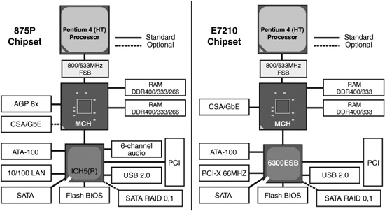
More advanced single-processor Pentium 4 servers from Intel and third parties use the E72xx chipsets, which combine server-specific features with some of the latest developments found in the 8xx and 9xx chipsets for desktop computers. Table 3.12 compares the features of the E7210, E7221, and E7230 chipsets.
Table 3.12 E72xx Chipsets for Pentium 4–Based Servers
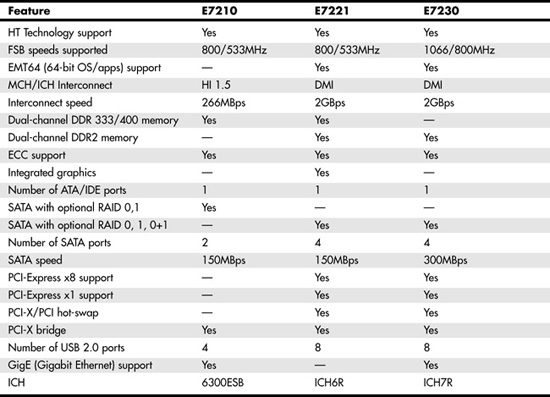
Note
Although the E7210 chipset was designed for the Pentium 4, some vendors have used it to create motherboards that support dual Xeon processors.
The 955X and 975X chipsets in Table 3.11 also support the dual-core Pentium D and Pentium Extreme Edition processors. The E7230 in Table 3.12 chipset also supports the dual-core Pentium D processor.
Table 3.13 compares the features of the ICH chips used by the chipsets listed in Tables 3.11 and 3.12.
Table 3.13 ICH Chips for Pentium 4 Server-Capable Chipsets1
The Intel 845 Family of Chipsets
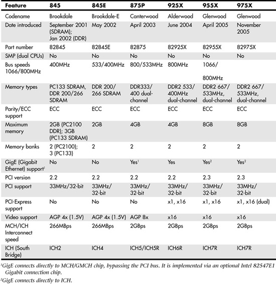
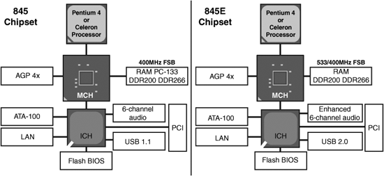
The 845 family of chipsets is widely used by both Intel and third-party motherboard makers for both entry-level servers and desktop computers. If you purchased a Pentium 4 system from late 2001 through mid-2003, it probably used some version of the 845 chipset. The 845, codenamed Brookdale during its development, was the first Pentium 4 chipset from Intel to support low-cost SDRAM instead of expensive RDRAM. Subsequent variations support DDR SDRAM at speeds up to DDR333, ATA-100, and USB 2.0.
The 845-series chipset is suitable for use in servers, including the 845 and 845E models. All members of the 845 family use the same hub-based architecture developed for the 8xx family, but they also have onboard audio and support the communications and networking riser (CNR) card for integrated modem and 10/100 Ethernet networking. However, they differ in their support for different types and amounts of memory, integrated graphics, external AGP support, and which ICH chip they use.
Although the original version of the 845 supported only PC133 SDRAM memory, the so-called 845D model (a designation used by review sites but not by Intel) also supports 200/266MHz DDR SDDRAM. The Intel 845's 82845 MCH supports Socket 478–based Celeron or Pentium 4 processors and can support up to two DDR SDRAM modules or three standard SDRAM modules (depending on the motherboard). When DDR SDRAM is used, the 845 supports either 200MHz (PC2100) or 266MHz (PC2700) memory speeds, with an FSB speed of 400MHz. The 845 also supports ECC error correction when parity-checked memory modules are used and offers an AGP 4x video slot, but it has no onboard video.
The 845 uses the same ICH2 chip (82801-BA) used by the Intel 850 and 850E chipsets in Rambus-based systems and the 815EP in low-cost SDRAM-based systems. The ICH2 supports ATA-100 hard disk interfacing, basic AC '97 sound, and four USB 1.1 ports.
The 845E is an updated version of the 845D with ECC error correction and support for 533MHz FSB, and it uses the enhanced ICH4 82801DB, which offers six USB 2.0 ports as well as integrated networking and enhanced 20-bit audio.
Figure 3.14 compares the system block diagrams of the 845 and 845E models.
Figure 3.14 The 845E (right) adds support for faster FSB speeds, memory, and USB 2.0 to the basic 845 chipset architecture (left).
The Intel 875P Chipset
The Intel 875P chipset, codenamed Canterwood during its development, was introduced in April 2003. The 875P chipset supports Intel's Hyper-Threading (HT) Technology, so it fully supports 3.06GHz and faster Pentium 4s, including the newer Prescott (90nm) core versions.
For faster memory access, the 875P supports four standard or ECC memory modules (up to 4GB total) using DDR333 or DDR400 memory in a dual-channel mode, and it offers a new Turbo mode that uses a faster path between DDR400 memory and the MCH to boost enhanced performance. Because multiple memory modules aren't always the same size or type, the 875P also features a new dynamic mode that optimizes system memory when different types or sizes of memory are used at the same time. The 875P also includes both SATA and RAID support and uses the same ICH5/ICH5R family used by the 865 series.
The Intel 925X Chipset
The Intel 925X chipset, codenamed Alderwood before its release, was released in 2004 as a replacement for the 875P Canterwood chipset. Unlike its predecessor, the 925X supports only DDR2 memory (up to 4GB maximum). The 925X supports the Pentium 4 Extreme Edition and the Pentium 4 processors in Socket 775 form factors.
The 925X supports PCI-Express x1 and PCI-Express x16 (video) as well as PCI version 2.3 expansion slots. It supports the LGA 775 processor socket and the Intel Prescott Pentium 4 core and uses the ICH6 family of South Bridge replacements detailed in Table 3.13. The 925X is widely used for single-processor server motherboards.
Intel 955X and 975X (Glenwood) Chipset Family
The Intel "Glenwood" chipset family, released in 2005, includes two members, the 955X and 975X. These chipsets are the first to support Intel's new dual-core Pentium D processors, and they also support the new high-performance single-core Pentium Extreme Edition processors as well as existing Pentium 4 HT Technology processors that use Socket 775. Although Intel categorizes these chipsets as "Entry-Level Workstation" and "Performance PC" chipsets, some vendors use these chipsets for single-processor workstation/server designs.
Although these chipsets are numbered in different series, most of their features are identical. Both support FSB speeds of 800MHz and 1066MHz and support up to four DDR2 667/533MHz memory modules (two pairs of dual-channel modules), for a maximum memory size of 8GB. Both support ECC memory, a must for server operation, and both use the ICH7 family of ICH chips listed in Table 3.13.
The 955X and 975X differ from each other in their video support. The 955X supports a single PCI-Express x16 video card, whereas the 975X supports two PCI-Express video cards in x8 mode, such as the ATI CrossFire series of graphics cards.
Alternatives to 955X/975X–Based Servers
Although you can use 955X or 975X chipsets in a server motherboard, servers don't need the high-performance graphics support they provide. Motherboards based on the E7230 chipset provide support for more memory than the 955X and 975X, optional support for PCI-X, and matrix RAID storage. The E7230's PCI slots can be used for video.
The E7210 Chipset
The Intel E7210 chipset, codenamed Canterwood-ES, during its development, was introduced in February 2004. Like the 875P, the E7210 supports Socket 478 Pentium 4 processors, including those featuring Intel's HT Technology and 800MHz FSB. It supports both Northwood (130 nm) and Prescott (90nm) core versions at clock speeds up to 3.4GHz.
The E7210 supports four standard or ECC memory modules (up to 4GB total) using DDR400 or DDR333 memory modules in a dual-channel configuration. The E7210 uses the 6300ESB ICH rather than the ICH5/ICH5R series used by the 8xx-series of server/workstation/desktop computer chipsets. The 6300ESB includes integrated support for PCI version 2.2 and 66MHz PCI-X slots. The E7210 supports up to two SATA (SATA) and two ATA-100 (ATA/IDE) drives, as well as four USB 2.0 ports. The PCI-X slots can be used for high-performance Gigabit Ethernet network adapters and SCSI RAID host adapters.
Figure 3.15 compares the architecture of the 875P and E7210 chipsets.
Figure 3.15 The E7210 (right) is based on the 875P (left) but adds support for PCI-X expansion slots.
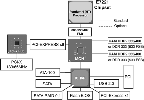
The E7221 Chipset
The Intel E7221 chipset, codenamed Copper River during its development, was introduced in September 2004. The E7221 supports Socket 775 Pentium 4 processors, enabling it to use the fastest and newest Pentium 4 processor designs on the market. The E7221 also supports Intel Extended Memory 64 Technology (EM64T), enabling systems based on this processor to support 64-bit operating systems such as Windows Server 2003 x64 Edition and various Linux distributions, as well as 32-bit operating systems, at full processor speed.
The E7210 supports four standard or ECC memory modules (up to 4GB total), using DDR2-533/400 or DDR400/333 memory modules in a dual-channel configuration. The E7210's MCH features a PCI-Express x8 interface. The PCI-Express x8 interface also supports the 6702PXH 64-bit PCI hub component of the chipset. When the 6702PXH chip is used as part of the E7221 chipset, the system also supports PCI-X expansion slots running at 64MHz or 133MHz.
The E7221 uses the ICH6R ICH, the same ICH used by the Intel 9xx desktop chipsets. The ICH6R provides SATA, PCI-Express x1, USB 2.0, PCI, and ATA-100 interfaces, and it connects to the MCH via the high-speed DMI interface. The E7221 is essentially a workstation and server version of the 9xx chipset.
The architecture of the E7221 chipset is shown in Figure 3.16.
Figure 3.16 The E7221 is based on the Intel 9xx chipsets, featuring PCI-Express.
The E7230 Chipset
The E7230 chipset, originally codenamed Mukilteo, was introduced in July 2005. Its basic design is similar to that of the E7221 chipset, but with several enhancements designed to support the newest processor and storage technologies.
The E7230 is the first Intel server chipset to support the dual-core Pentium D processor, enabling a single-processor server to have performance virtually the same as that of a two-way server, but at a lower cost. The E7230 also supports Intel matrix storage technology, enabling simultaneous RAID 0 (striping) and RAID 1 (mirroring) with only two disk drives and PCI-Express x8, x4, and x1 cards. By adding the 6702PXH 64-bit PCI-X hub, PCI-X cards, such as network and SCSI RAID adapters, are also supported.
The E7230 also supports Socket 775 Pentium 4 processors with HT Technology, Execute Disable Bit, and Intel Extended Memory 64 Technology (EM64T). The E7230 features a maximum memory size of 8GB, using only DDR2 memory modules in 667/533/400MHz speeds, arranged in a dual-channel configuration.
The E7230 uses the ICH7R ICH, the same ICH used by the Intel 955X and 975X desktop chipsets. The ICH7R provides SATA Matrix storage RAID, PCI-Express x1, USB 2.0, PCI, and ATA-100 interfaces, and it connects to the MCH via the high-speed DMI interface.
Intel ICH Chips for 9xx and E72xx Chipsets
Intel has used the ICH5, ICH5R, ICH6R, 6300ESB, and ICH7R ICH chips with its 8xx, 9xx, and E72xx chipsets for the Pentium 4. The following sections provide additional details about these chips.
The ICH5 and ICH5R I/O Controllers
ICH5 and ICH5R (RAID) are the Intel ICHs for its AHA and HI 1.5 hub-based architecture, which is the equivalent of the South Bridge in Intel's hub-based architecture introduced with the 800 series of chipsets.
ICH5 and ICH5R feature four USB 2.0 controllers with eight external ports, two ATA-100 ports, and two SATA-150 ports. ICH5R models add support for RAID 0 (striping) and RAID 1 (mirroring) on the SATA ports. ICH5 and ICH5R also support the PCI 2.3 bus and include an integrated 10/100 Ethernet LAN controller.
Note
RAID 1 (mirroring) support for ICH5R-equipped motherboards requires the installation of the latest version of the Intel Application Accelerator, RAID Edition. In some cases, you might also need to install the latest edition of the Intel RAID Option ROM first. For more information and to download driver and option ROM updates, go to http://support.intel.com/support/chipsets/iaa_raid/.
The 6300ESB I/O Controller
The 6300ESB I/O controller used in the E7210 chipset integrates support for four PCI-X 66MHz slots. It also features support for four PCI 2.2 slots, two SATA-150 ports (including RAID), four USB 2.0 ports, two ATA-100 ports, and AC '97 integrated audio.
The ICH6R I/O Controller
ICH6R is the RAID version of the Intel ICH used by the 9xx series of desktop chipsets as well as by the E7221 server/workstation chipset. ICH6R features four USB 2.0 controllers with eight external ports, one ATA-100 port, one 10/100 Ethernet port, four PCI-Express x1 slots, and four SATA-150 ports. The SATA ports support RAID 0, 1, and 10. The ICH6R also features high-definition audio.
The ICH7 and ICH7R I/O Controllers
ICH7 and ICH7R are the latest versions of Intel's ICH chips. They are based on ICH6/6R, but also feature 10/100/1000 Ethernet and SATA-300 ports. The ICH7R version features Matrix storage technology, which supports simultaneous RAID 0 and RAID 1 on two drives, and also supports RAID 0+1 support with four drives.
Intel Xeon DP and Xeon MP Chipsets
The Intel Xeon DP and Xeon MP processors are workstation and server-class processors based on the Pentium 4 processor, but they use a larger socket (Socket 603/604) and use the E75xx series of chipsets. The E75xx chipsets are improved versions of the 860 chipset, which was the first Xeon DP chipset.
The Intel 860 Chipset
The Intel 860 was a high-performance chipset designed for the first Socket 603 (Pentium 4–based) Xeon processors for DP workstations. The 860 uses the same ICH2 as the Intel 850 but uses a different MCH—the 82860, which supports one or two Socket 603 ("Foster") Xeon processors. The other major features of the 82860 are similar to those of the 82850, including support for dual 400MHz RDRAM memory channels with a 3.2GBps bandwidth and a 400MHz system bus. The 82860 MCH also supports 1.5V AGP 4x video cards at a bandwidth exceeding 1GBps.
The 860 chipset uses a modular design, in which its two core chips can be supplemented by the 82860AA (P64H) 66MHz PCI controller hub and the 82803AA MRHR. The 82860AA supports 64-bit PCI slots at either 33MHz or 66MHz, and the 82803AA converts each RDRAM memory channel into two, which doubles memory capacity. Thus, whether a particular 860-based motherboard offers 64-bit or 66MHz PCI slots or dual-channel RDRAM memory depends on whether these supplemental chips are used in its design.
The 860 chipset was replaced by the E7500 Plumas chipset in 2002.
The Intel E7500 Chipset
The Intel E7500 chipset, codenamed Plumas, was introduced in March 2002. It supports up to two Xeon processors with 512KB L2 cache, 400MHz FSB, and Intel HT Technology. The E7500's design is simpler than that used by the 860 because by 2002, Intel was no longer supporting RDRAM in new systems.
The E7500 chipset includes the MCH and the ICH3-S ICH. To achieve 66MHz/64-bit PCI and 133MHz PCI-X support, the E7500 can be used with up to three optional P64H2 (82870P2) chips, an improved version of the P64H chip that is an optional part of the 860 chipset. Note that the E7500's MCH connects directly to memory, rather than to MRHR chips as with the 860. The E7500's design is simpler than that used by the 860, because by 2002 Intel was no longer supporting RDRAM in new systems. The E7500 supports up to 16GB of dual-channel DDR200 registered ECC SDRAM memory (up to eight modules). Its Intel x4 single-device data correction (SDDC) can correct up to four errors per memory module for better system reliability. Hub Architecture 2.0 provides a 2GBps bidirectional connection between the E7500 MCH and each P64H2 chip.
The E7500, and its sibling, the E7501 (described in the next section), have been used in many two-way servers.
The Intel E7501 Chipset
The Intel E7501 chipset, codenamed Plumas 533, was introduced in November 2002. It represents an improved version of the E7500, differing primarily in support for the 533MHz FSB versions of Xeon processors and support for dual-channel DDR266 memory. The E7501 also uses the same P64H2 and ICH-3S chips as the E7500.
Figure 3.17 depicts the architecture of the E7501 chipset.
Figure 3.17 The E7501 is a faster version of the E7500; both support two Xeon processors.
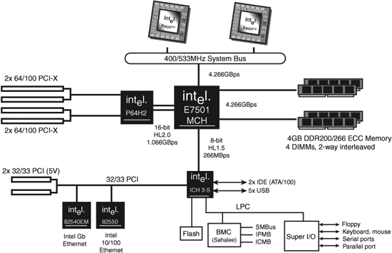
The Intel E7505 Chipset
The Intel E7505 chipset, codenamed Placer, was introduced in November 2002. It supports up to two Xeon processors with 512KB L2 cache, 533MHz FSB, and Intel HT Technology.
The E7505 supports 1.5V AGP 1x–8x and AGP Pro cards (but not the nonstandard 3.5V versions of AGP once sold by some vendors), and it uses the ICH4. To achieve 66MHz/64-bit PCI and 133MHz PCI-X support, the E7505 can be used with up to three optional P64H2 (82870P2) chips. The E7505 uses the ICH4. The E7505 has been used in many two-way server and workstation designs.
Figure 3.18 illustrates the architecture of the E7505 chipset.
Figure 3.18 The E7505 supports AGP 8x, making it suitable for workstation as well as server applications.
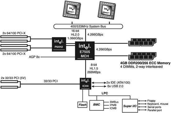
The Intel E7520 and E7320 Chipsets
The Intel E7520 chipset, codenamed Lindenhurst, was introduced in August 2004. Its companion, the E7320 chipset, codenamed Lindenhurst VS, was introduced at the same time. Both chipsets support up to two 64-bit (EM64T) Xeon processors with 2MB L2 cache, 800MHz FSB, and Intel HT Technology or Xeon processors with 1MB L2 cache and 800MHz FSB.
These chipsets support dual-channel DDR2-400 or DDR 333/266 memory and can be used with either the ICH5R or 6300ESB ICHs.
The E7520 differs from the less-expensive E7320 by offering memory mirroring as well as DMA support in the memory subsystem. Both chipsets support ECC memory, X4 SDDC, and hub interface ECC for reliable memory access.
![]() See "Advanced Error Correction Technologies," p. 391.
See "Advanced Error Correction Technologies," p. 391.
The E7520 includes three PCI-Express x8 interfaces, and the E7320 includes one PCI-Express x8 interface. The x8 interfaces can be configured as two PCI-Express x4 interfaces, which act as hosts for optional 6700 PXH 64-bit PCI hubs that provide 66MHz PCI-X or PCI interfaces with hot-plug support. The E7520 also supports the IOP332 I/O processor chip (codenamed Dobson), designed for high-performance RAID implementations. Figure 3.19 illustrates a typical block diagram for a system running an E7520/6300ESB chipset.
Figure 3.19 The E7520 supports PCI-X and PCI-Express interfaces, enabling it to operate with the latest high-speed I/O boards for SCSI RAID, networking, and other applications.
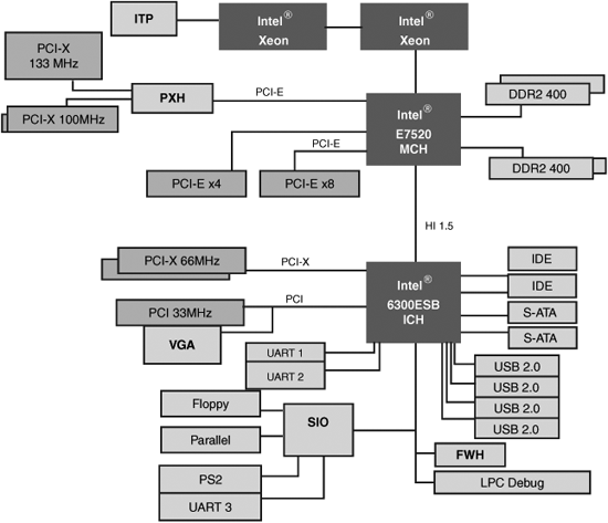
The Intel E8500 Chipset
The Intel E8500 chipset, codenamed Twin Castle before its release, was introduced in April 2005. It supports up to four of the latest dual-core Xeon MP processors as well as existing single-core processors, and it supports Intel's EM64T extensions, enabling this chipset to support 64-bit or 32-bit server operating systems. When dual-core Xeon MP processors are used, the system is essentially an eight-way system.
The E8500 chipset includes the following components:
- E8500 North Bridge
- E8500 XMB
- 6700PXH 64-bit PCI hub (supports PCI and PCI-X slots up to 133MHz)
- ICH5 (equivalent to the South Bridge)
Despite Intel's use of the term "North Bridge," the E8500 uses a hub architecture to connect to the ICH5.
The E8500 North Bridge supports PCI-Express, providing three x8 lanes and four 1x lanes. PCI-Express support enables the E8500 to use newly emerging and forthcoming PCI-Express interfaces for high-speed networking, SCSI RAID arrays, and other server-optimized components.
The E8500 supports DDR266, DDR333, and DDR-2 400 memory via one or more high-speed IMI connections to the 8500's XMB memory bridge chips (see Figure 3.20). It supports registered ECC DIMMS and features memory RAID (similar to memory mirroring) and demand and patrol scrubbing to detect and repair memory problems. If it encounters a memory problem that cannot be repaired, it marks the bad location so that it will not be used in the future. The IMI interconnect runs at 2.67GBps inbound and 5.33GBps outbound.
Figure 3.20 The E8500 combines the hub architecture of the 8xx-series chipsets with specialized memory controller and PCI-Express bridge chips to support a powerful four-way architecture.
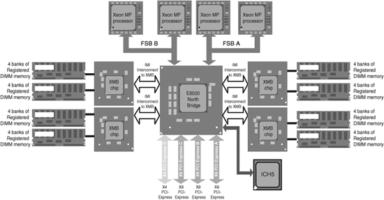
Intel Itanium and Itanium 2 Chipsets
Intel's first 64-bit server processors are the Itanium and Itanium 2 processor families. The 64-bit architecture of these processors is a completely different architecture than the 32-bit or x64 extensions to 32-bit processor architectures supported by the Intel Pentium series and AMD Athlon series. (See Chapter 2 for more information.)
Intel's first chipset for the Itanium, the 460GX, was introduced in June 2001, coinciding with the initial release of the Itanium processor. The 460GX chipset included 10 components, enabling developers to customize Itanium systems for use as workstations with AGP4x graphics or as servers with up to four Itanium processors. The original Itanium was quickly replaced by the Itanium 2 because the Itanium's lengthy development time basically made it obsolete by the time it was delivered. The Itanium 2 offers faster clock speeds and larger memory caches than the original Itanium.
The current Intel Itanium 2 chipset is the E8870, which supports up to four Itanium 2 processors. When equipped with the E8870SP scalability port switch component, the E8870 supports up to eight Itanium 2 processors. The E8870 was introduced in August 2002.
The following sections provide detailed information about these chipsets.
The Intel 460GX Chipset for Itanium
The Intel 460GX chipset, the first (and only) chipset developed by Intel for the first-generation Itanium processor, was scarcely a chipset in the established sense of the term. Instead of using a relatively small number of versatile chips, the Intel 460GX seemed to use a different chip for almost every significant task performed outside the processor. As a result, the 460GX chipset includes a total of 10 components:
- 82461GX—The System Address Controller (SAC) interfaced memory and control lines between memory and the Itanium processors via the MAC chips.
- 82462GX—The System Data Path Controller (SDC) interfaced data lines between memory and the Itanium processors via the MDC chips.
- 82463GX—The Memory Address Controller (MAC) connected system memory to the SAC.
- 82464GX—The Memory Data Controller (MDC) connected system memory to the SDC.
- 82465GX—The Graphics Expansion Bus (GXB) provided an AGP 4x expansion slot (for workstation use).
- 82466GX—The Wide and Fast PCI Expansion Bus (WXB) supported two independent 66MHz, 64-bit PCI interfaces to the SAC.
- 82467GX—The PCI eXpander Bridge (PXB) provided two 32-bit, 33MHz PCI interfaces or a single 64-bit, 33MHz PCI interface to the SAC.
- 82468GX—The I/O and Firmware Bridge (IFB) provided a PCI-to-ISA bridge, USB ports, the interface to the FWH, the interface to the Super I/O chip, and other support functions. It connected to the PXB.
- 82802AC—The Firmware Hub (FWH) stored firmware (BIOS) and security features. It connected to the IFB.
- 82094AA—The Programmable Interrupt Device (PID) was an interrupt controller with steering capabilities. It was actually an NEC-developed part (NEC #UPD66566S1-016).
Figure 3.21 illustrates the architecture of a four-way system using the 460GX chipset.
Figure 3.21 The 460GX used many single-purpose chips instead of highly integrated chips to support the original Itanium processor.
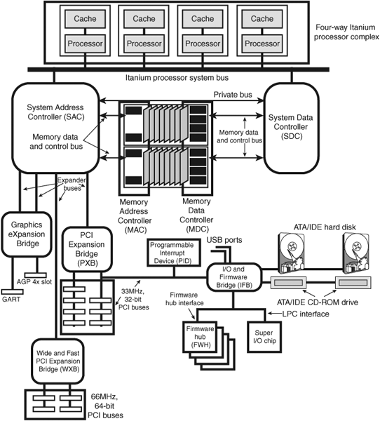
Very few servers were built using the Itanium processor or the 460GX chipset. However, the 460GX chipset is significant for being the most complex Intel chipset to date.
The Intel E8870 Chipset for Itanium 2
The Itanium 2 processor rapidly replaced the original Itanium processor, and because of major changes in its design, a brand-new chipset was needed. The E8870 was introduced at the same time as the Itanium 2, and it continues to be Intel's only Itanium 2–compatible chipset. (Other vendors have also produced Itanium 2 chipsets.)
Note
The E8870 was designed during the period in which Intel had selected RDRAM as its preferred memory technology. However, by the time the E8870 was introduced, it had become obvious that RDRAM was more expensive than DDR SDRAM and did not offer performance commensurate with its higher cost. Thus, Intel decided to add a DDR memory hub component to the E8870 to convert DDR SDRAM signals to RDRAM signals compatible with the SNC's built-in memory controller. While this adds several chips to typical E8870 implementations, servers based on the E8870 can now use reasonably priced registered DDR SDRAM instead of expensive RDRAM.
Unlike the 460GX, the E8870 (also known as the 870) uses Intel's modern hub architecture along with specialized support chips. The E8870's components include the following:
- E8870—The Scalable Node Controller (SNC) provides memory controller and system bus interfacing services. It can be connected to the SPS for scaling to dual-node (eight-way) implementations, or it can connect to the SIOH for single-node (four-way and smaller) implementations. It receives DDR memory signals through connections to DMH chips.
- E8870DM—The DDR Memory Hub (DMH) translates two DDR channels into the native quad-channel Rambus memory bus on the SNC.
- E8870IO—The Server Input/Output Hub (SIOH) provides an HI 1.5 (266Mbps) connection to the ICH4 and provides dual HI 2.0 (1Gbps) connections to the P64H2 PCI-X bridges.
- 82870P2—The 64-bit PCI/PCI-X Controller (P64H2) supports 64-bit PCI-X slots running at 133MHz. (PCI-X also supports PCI devices.) It can be used to support Intel Gigabit Ethernet and Intel I/O processor chips.
- 82801DB—The ICH (ICH4) supports USB 2.0, ATA/IDE, and other legacy ports.
- 80802AC—The Firmware Hub (FWH) supports BIOS and security features.
These components are used in four-way Itanium implementations; each four-way implementation is known as a node. However, an additional component, known as the E8870SP, the Scalability Port Switch (SPS), is used to connect two nodes into an eight-way implementation. The SPS was introduced after the initial release of the E8870 chipset.
Figure 3.22 illustrates the architecture of a typical four-way Itanium 2 system using the E8870, and Figure 3.23 illustrates how the SPS is used to enable eight-way processing.
Figure 3.22 The E8870's architecture in a typical four-way implementation.
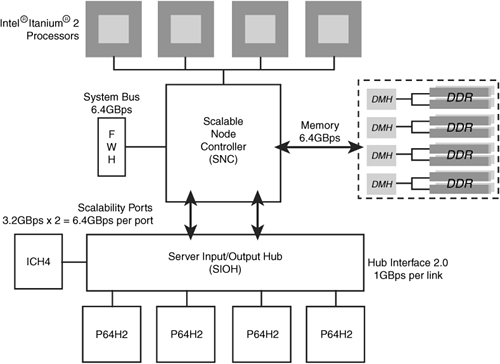
Figure 3.23 The E8870's architecture when SPS chips are used to create a two-node (eight-way) system. Note that one SPS chip is used for each node.
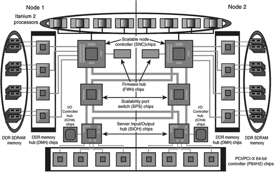
Broadcom ServerWorks Chipsets for Intel Processors
Starting in 1997, ServerWorks (a Broadcom company originally known as Reliance Computer Corporation) introduced its first server chipsets for Intel processors. Today, ServerWorks is second only to Intel as the major supplier of server chipsets for Intel-based servers.
Early ServerWorks chipsets included the ServerSet I (also known as the Champion 1.0 chipset) and the ServerSet II. ServerSet I supported up to six Pentium Pro processors and featured two 32-bit PCI buses. ServerSet II supported up to four Pentium II Xeon processors and featured a 64-bit PCI bus. These chipsets were discontinued several years ago.
Current ServerWorks chipsets support the Pentium III Xeon and Xeon DP and MP (based on Pentium 4) processors. Although ServerWorks uses the North Bridge and South Bridge terminology for its chipsets, its current chipsets also include memory controller and I/O bridge chips. Thus, ServerWorks chipsets more closely resemble E7xxx-series Intel chipsets than Intel's 8xx or 9xx chipsets.
Several major motherboard and system builders, including Intel, have used Champion- and Grand Champion–series chipsets for multiprocessor server motherboards and systems.
Note
For more information about ServerWorks chipsets, see the Broadcom website, at www.broadcom.com.
ServerWorks Chipsets for Intel Pentium III Xeon Processors
ServerWorks currently makes three chipsets for the Pentium III Xeon processors:
- Champion HE (also known as Champion Enterprise)—Supports up to four processors with 100MHz FSB; the North Bridge is the NB6536 2.0HE.
- Champion HE-SL (also known as Champion Volume)—Supports up to two processors with 133/100MHz FSB; the North Bridge is the NB6576.
- Champion LE (also known as Champion Entry)—Supports up to two processors with 133/100MHz FSB; the North Bridge is the NB6635 3.0LE.
Originally, this series of chipsets was known as the ServerSet III series.
All three North Bridge chips can be paired with either the OSB4 or CSB5 South Bridge chip to form a chipset. The OSB4 features UDMA/33 ATA/IDE hard disk host adapter, USB 1.1 ports, and an LPC connection to a Super I/O chip. The CSB5 features an UDMA/100 ATA/IDE hard disk host adapter, USB 1.1 ports, and an LPC connection to a Super I/O chip. Most motherboards that use a Champion-series chipset use SCSI-based hard disks or RAID arrays instead of ATA hard disks, so there is little practical difference between these South Bridge chips.
Table 3.14 provides an overview of the Champion series of chipsets for the Pentium III Xeon processor.
Table 3.14 Champion Chipsets for Pentium III Xeon
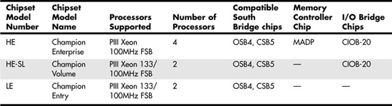
The Champion LE Chipset
The Champion LE chipset is the simplest of the current Champion series, using only North Bridge and South Bridge chips. For greater reliability than with desktop-adapted chipsets, Champion LE, like all current ServerWorks server chipsets, uses registered memory.
Champion LE supports two 64-bit/66MHz PCI expansion slots via the South Bridge chip. However, if you need additional 64-bit slots, Champion LE is not a suitable choice. Thus, Champion LE is best suited to basic dual-processor server applications.
The Champion HE-SL Chipset
Although the Champion HE-SL chipset supports two processors, as does the Champion LE, it is a more powerful and flexible chipset. It supports AGP 2x graphics, and ECC registered memory must be installed in matched pairs to support memory interleaving for better memory performance.
However, the most significant improvement in Champion HE-SL over its Champion LE sibling is its support for both 3.3V (66MHz) and 5V (33MHz) 64-bit PCI slots. This comes via the third component in the HE-SL chipset, the CIOB20 I/O bridge. The CIOB20 (also known as the NB6555 IO Bridge 2.0 chip), provides a 64-bit PCI bridge between the North Bridge and 64-bit PCI slots. The connection to the North Bridge uses ServerWorks's own Inter Module Bus (IMB) high-speed connection. IMB runs at 1GBps, which is four times faster than Intel's Hub Architecture 1.0 or 1.5 or the VIA V-Link 4x interconnections.
If you need to use several PCI cards (33MHz or 66MHz) in a server, the Champion HE-SL is a better choice than the Champion LE.
The Champion HE Chipset
The Champion HE is the most powerful of the Champion series. It supports four Pentium III Xeon processors and uses a fourth ServerWorks chipset component, the MADP memory controller chip. In a four-way configuration, four MADP chips are used, but in a two-way configuration, only one MADP chip is used (see Figure 3.24).
Figure 3.24 The ServerWorks Champion HE chipset in a typical four-way configuration.
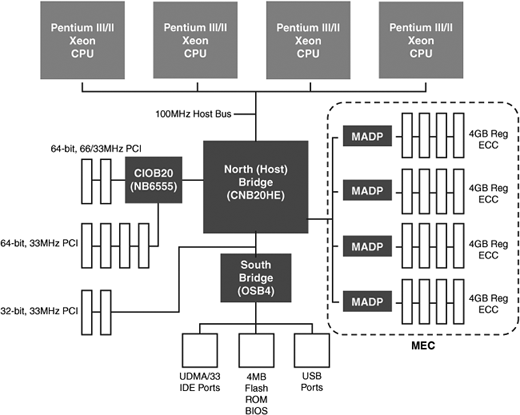
The MADP chip supports memory interleaving for better memory performance in both two-way and four-way configurations.
ServerWorks Chipsets for Intel Xeon Processors
ServerWorks currently makes three chipsets for the Xeon processors based on the Pentium 4:
- Grand Champion HE (also known as Grand Champion Enterprise)—Supports up to four processors with 400MHz FSB; the North Bridge chip is called CMIC-HE.
- Grand Champion LE (also known as Grand Champion Volume)—Supports up to two processors with 533/400MHz FSB; the North Bridge chip is called CMIC-SL.
- Grand Champion SL (also known as Grand Champion Entry)—Supports up to two processors with 533/400MHz FSB; the North Bridge chip is called CMIC-LE.
Originally, this series of chipsets was to be known as the ServerSet IV series.
All three North Bridge chips can be paired with either the CSB5 or CSB6 South Bridge chip to form a chipset. The CSB6 is the most advanced South Bridge chip used by any ServerWorks chipset to date. It includes three ATA-100 ATA/IDE host adapters; support for ATA RAID 0, 1, and 5; 64-bit PCI bus; 400MBps connection to the North Bridge; and USB 1.1 ports.
Table 3.15 provides an overview of the Grand Champion series of chipsets for Xeon processors.
Table 3.15 Grand Champion Chipsets for Intel Xeon
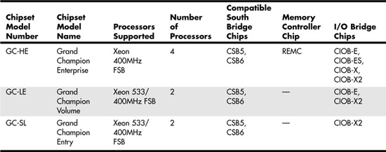
The GC-SL (Grand Champion Entry) Chipset
The Grand Champion SL chipset is the simplest of the current Grand Champion series. Its North Bridge chip incorporates a single IMB I/O interface and a single Thin-IMB interface to the South Bridge. It supports up to 4GB of RAM. RAM contents are protected with 128-bit ECC and spare memory technologies. The optional CIOB-E bridge provides Gigabit Ethernet support, while the optional CIOB-X2 I/O bridge provides PCI-X support up to 133MHz. In its basic North Bridge/South Bridge configuration, Grand Champion SL is suitable for basic server designs. However, when the CIOB-X2 PCI-X bridge is added, it is also suitable for midrange server designs.
The GC-LE (Grand Champion LE) Chipset
The dual-processor Grand Champion LE is designed to handle four times the memory (16GB) of the Grand Champion SL. It also supports two CIOB-X2 PCI-X I/O bridge chips, enabling a motherboard to have up to six PCI-X 100/66MHz cards, up to three PCI-X 133MHz cards or a mix of PCI-X cards and onboard devices. Thus, if you need support for several PCI-X cards, or a mix of PCI-X cards, a high-speed integrated SCSI host adapter and a Gigabit Ethernet adapter as in Figure 3.25, the Grand Champion GC-LE chipset is a better choice than the GC-SL.
Figure 3.25 A typical implementation of the Grand Champion LE server chipset.
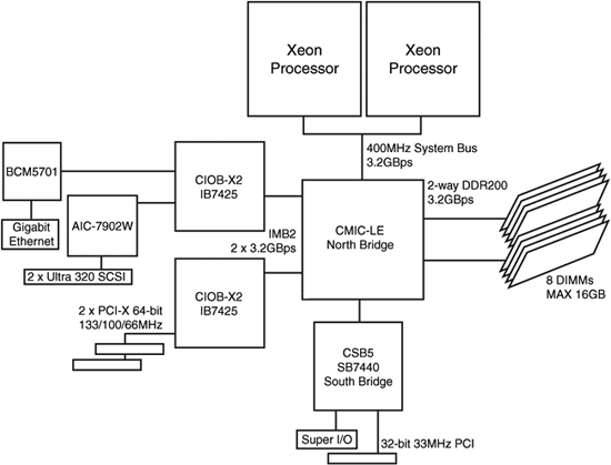
Figure 3.25 illustrates the block diagram of a typical server using the GC-LE chipset.
The GC-HE (Grand Champion HE) Chipset
The Grand Champion HE is the most powerful of the Grand Champion series. It supports four Xeon MP processors and incorporates three IMB I/O interfaces for the fastest memory interfacing of any GC-series ServerWorks chipset. With support for up to 64GB of memory, its memory contents are protected with 128-bit ECC, chipkill, spare memory, memory mirroring, and hot-plug memory card support technologies. The GC-HE uses five REMC memory controller chips in a four-way configuration: four in the data path and a fifth one in the address path.
Figure 3.26 illustrates a four-way implementation of the GC-HE chipset.
Figure 3.26 A typical implementation of the Grand Champion HE server chipset.
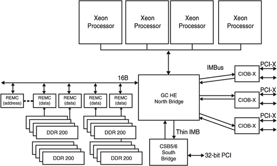
ServerWorks South Bridge and Support Chips
All ServerWorks Champion and Grand Champion chipsets contain South Bridge chips, and many of them also contain I/O bridge and memory controller chips. The South Bridge chips used by ServerWorks chipsets support ATA/IDE, PCI, and legacy I/O devices. Table 3.16 provides more information about the South Bridge chips used with Champion and Grand Champion chipsets.
Table 3.16 Champion/Grand Champion South Bridge Chips
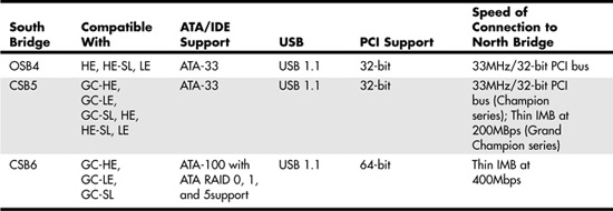
The I/O bridge chips provide support for PCI-X slots and, in some versions, Gigabit Ethernet. Table 3.17 provides more information about the I/O bridges used by the Champion and Grand Champion chipsets.
Table 3.17 Champion/Grand Champion I/O Bridge Chips
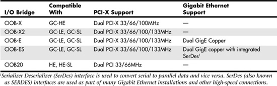
The high-end HE and GC-HE chipsets also use memory controller chips to provide support for memory interleaving. Memory interleaving divides memory into banks, permitting memory to be accessed more quickly for improved performance. Table 3.18 provides more information about these chips.
Table 3.18 Champion/Grand Champion Memory Controller Chips
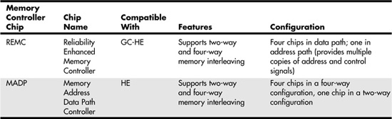
Other Third-Party Server Chipsets for Intel Processors
Although Intel and ServerWorks are the major producers of server-class chipsets for Intel server processors, they are not the only producers of these chipsets.
Other vendors, including VIA Technologies, IBM, and Hewlett-Packard have also produced server-class chipsets for Intel processors from the Pentium Pro and Pentium II through the Itanium 2. The following sections discuss the offerings from these companies.
VIA Technologies Chipsets for Intel Server Processors
Although VIA Technologies built a variety of chipsets for the P6 family of processors, only the following have been used in one-way and two-way servers:
- Apollo Pro 133A with VIA 694MP North Bridge (two-way servers) with VIA VT82694X (one-way servers)
- Apollo Pro 266/266T
Table 3.19 provides an overview of these chipsets.
Table 3.19 VIA Server-Class Chipset for P6 Processors
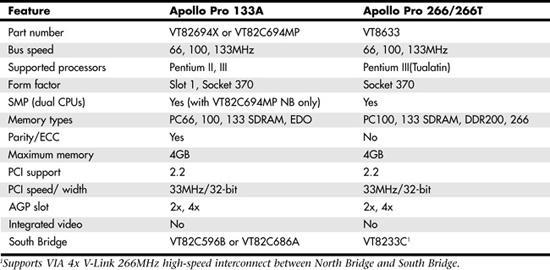
Although some of VIA Technologies Pentium 4–class chipsets are also compatible with the Xeon, litigation has discouraged motherboard makers from adopting them for server-class motherboards.
The VIA Technologies Apollo Pro 133A Chipset
The VIA Apollo Pro133A chipset was a North Bridge/South Bridge chipset designed to support Slot 1 and Socket 370 processors such as the Intel Pentium III, Intel Celeron, and VIA Cyrix III. The Apollo Pro133A is based on the previous Pro133, with additional features added. Note that there are actually two versions of this chipset. The original version was released in fall 1999 and supported single-processor installations and used the VIA 694 North Bridge. In spring 2000, VIA Technologies developed a dual-processor–compatible version using the 694MP North Bridge.
Features of the Apollo Pro133A include the following:
- AGP 4x graphics bus support
- 133/100/66MHz processor bus support
- PC-133 SDRAM memory interface
- UltraATA/66 interface
- Support for four USB 1.1 ports
- AC '97 link for audio and modem
- Hardware monitoring
- Power management
The VIA Apollo Pro133A chipset was a two-chip set consisting of the VT82C694X North Bridge controller (single-CPU version) or VT82C694MP North Bridge controller (dual-CPU version) and a choice of a VT82C596B or VT82C686A South Bridge controller.
Table 3.20 provides an overview of the features of the South Bridge chips used in the Apollo Pro 133A chipset.
Table 3.20 VIA South Bridge Chips Used with Apollo Pro 133A
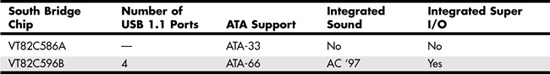
A number of vendors produced dual-processor server motherboards using the Apollo Pro 133A chipset.
The VIA Technologies Apollo Pro266 Chipset
The VIA Apollo Pro266 is a high-performance North Bridge/South Bridge chipset designed to support Socket 370 processors, including the Pentium III. The Apollo Pro266 was the first chipset from VIA to replace the traditional PCI (133MBps) connection between North Bridge and South Bridge chips with VIA's 4x V-Link interconnect, which runs at 266MBps. The Apollo Pro 266 was introduced in late 2000.
Features of the Apollo Pro266 include the following:
- AGP 2x/4x graphics bus support
- 133/100/66MHz processor bus support
- PC-100/133 SDRAM and PC200/266 DDR SDRAM memory interface
- ATA-100 IDE interface
- Support for six USB 1.1 ports
- Integrated AC '97 six-channel audio
- Integrated MC '97 modem
- Integrated 10/100BASE-T Ethernet and 1/10MHz Home PNA networking
- Hardware monitoring
- ACPI/On Now! power management
- VIA 4x (266MBps) V-Link North Bridge/South Bridge interconnect
The VIA Apollo Pro266 chipset was a two-chip set consisting of the 552-pin BGA VT8633 North Bridge controller and the 376-pin BGA VT8233 South Bridge controller. The Apollo Pro266T is an updated version of this chipset that supports Pentium III Tualatin processors. Figure 3.27 shows the architecture of the Apollo Pro266 chipset.
Figure 3.27 Apollo Pro266 chipset architecture.
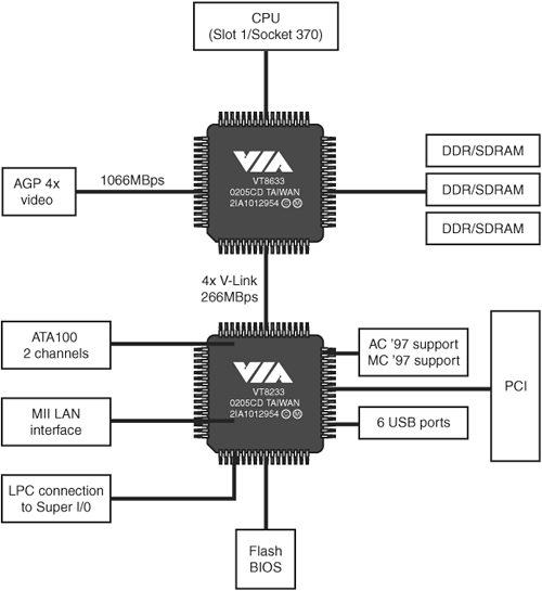
Because of the V-Link high-speed interconnect between the North Bridge and South Bridge, PCI is managed by the South Bridge. This is similar to the way in which Intel Hub Architecture works, and this basic architecture has been followed by all subsequent VIA chipsets that use V-Link architecture.
The Apollo Pro 266 and 266T (Tualatin-compatible version) chipsets have been used by a variety of vendors to produce both standard ATX form factor and various types of single-board–computer servers using one or two processors.
IBM Chipsets for Intel Server-Class Processors
IBM has produced several chipsets for its own lines of Intel server-class processors:
- XA-32 (Summit)—Supports 32-bit Xeon processors.
- XA-32 second-generation—Supports 32-bit Xeon processors.
- XA-64—Supports Itanium 2 processors.
- XA-64e (Hurricane)—Supports 64-bit Xeon processors. The following sections provide details of these chipsets.
The XA-32 Chipset for Xeon MP/DP
IBM's XA-32 chipset, codenamed Summit, was first fully implemented in the IBM @server xSeries 440, released in September 2002. This chipset, developed by the IBM Microelectronics Division in Austin, Texas, has the following major features:
- Support for Xeon MP Foster processors for two-way, four-way, or eight-way implementations
- Support for Xeon DP Prestonia processors for two-way or four-way implementations (the XA-32 chipset permits four-way operation with Xeon DP processors, although Intel designed the Xeon DP for single- or two-way operation only)
- Support for memory mirroring, chipkill, and Memory ProteXion features for memory reliability
- Support for 64-bit PCI-X slots at 133MHz, 100MHz, and 66MHz speeds
The components of the XA-32 chipset include the following:
- The Cyclone memory controller—Each four-way installation requires a memory controller. The memory controller is located in the SMP expansion module.
- The Twister processor and cache controller—Each eight-way installation requires a cache controller. The processor and cache controller is located in the SMP expansion module.
- Two Winnipeg PCI bridges—The PCI bridges are connected to the Cyclone memory controller. Typically, one PCI bridge is used for interfacing to 133MHz and 100MHz PCI-X slots, and the other PCI bridge is used for interfacing to 66MHz PCI-X slots, video, USB, keyboard/mouse, SCSI, Gigabit Ethernet, and other I/O devices, as well as the Remote Expansion I/O (RXE) port. The RXE port connects to the optional RXE-100 enclosure, which supports 12 PCI-X slots.
Figures 3.28 and 3.29 show the major components of the XA-32 chipset in a 4-way (top) and 8-way (bottom) configuration, respectively. Each 8-way configuration is called a node, and two nodes can be connected via the SMP expansion ports to create a 16-way processor complex.
Figure 3.28 Four-way configuration using the IBM XA-32 chipset.
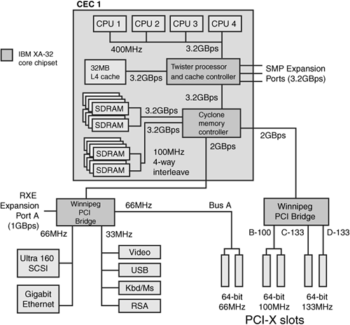
Figure 3.29 Eight-way configurations using the IBM XA-32 chipset.
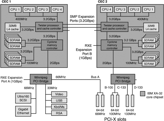
The XA-32 Second-Generation Chipset for Xeon MP/DP
The second generation of the IBM XA-32 chipset is used in IBM xSeries servers such as the x365, x445, and x455. It has the following major differences from the original XA-32:
- Improved Cyclone memory controller (version 3.0) for lower memory latency than in the original XA-32 chipset.
- Improved Winnipeg PCI bridges (version 4.0) that support 133MHz PCI-X expansion slots.
- Support for Gallatin versions of the Xeon MP processor. Gallatin versions of the Xeon MP run at speeds up to 3GHz.
![]() See "Xeon Processors," p. 114.
See "Xeon Processors," p. 114.
The block diagram shown in Figure 3.28 applies to both original and second-generation XA-32–based systems.
The XA-64 Chipset for Itanium 2
The IBM XA-64 chipset, codenamed Summit, was first used in the xSeries 450 server released in mid-2003. It was developed by the IBM Microelectronics Division. It has the following major features:
- Support for one to four Itanium 2 Madison processors
- Support for memory mirroring, chipkill, and Memory ProteXion features for memory reliability
- Support for 64-bit PCI-X slots at 133MHz, 100MHz, and 66MHz speeds
The components of the XA-64 chipset include the following:
- The Cyclone memory controller—The memory controller is located in the memory-board assembly.
- The Tornado processor and cache controller—The processor and cache controller is located in the processor board assembly. It connects to the processors as well as to 64MB of L4 cache, a feature IBM calls XceL4 Server Accelerator Cache.
- Two Winnipeg PCI bridges—The PCI bridges are connected to the Cyclone memory controller. Typically, one PCI bridge is used for interfacing to 133MHz and 100MHz PCI-X slots, and the other PCI bridge is used for interfacing to 66MHz PCI-X slots, video, USB, keyboard/mouse, SCSI, Gigabit Ethernet, and other I/O devices, as well as the RXE port. The RXE port connects to the optional RXE-100 enclosure, which supports 12 PCI-X slots.
Figure 3.30 shows the major components of the XA-64 chipset in a four-way configuration.
Figure 3.30 A typical four-way configuration using the IBM XA-64 chipset.
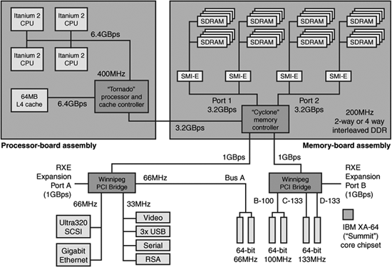
The XA-64e Chipset for 64-Bit Xeon Processors
IBM's XA-64e chipset, codenamed Hurricane, is used in Xeon EM64T-compatible IBM @servers such as the xSeries 366. This chipset, developed by the IBM Microelectronics Division in Austin, Texas, has the following major features:
- Support for one to four Xeon MP Cranford processors supporting EM64T (Intel's term for 64-bit extensions to IA-32 architecture)
- Support for memory mirroring (works with hot-swapping), chipkill, and Memory ProteXion features for memory reliability
- Support for memory hot-swapping or hot-adding (hot-adding requires that memory mirroring be disabled)
- Support for 64-bit PCI-X 2.0 Active PCI slots running at 266MHz.
![]() See "Xeon MP with EM64T Support," p. 120.
See "Xeon MP with EM64T Support," p. 120.
The components of the XA-64e chipset include the following:
- The Hurricane memory and I/O controller—The memory controller provides a one-chip interface between the processor(s), memory, and the Winnipeg PCI-X bridge chips. Memory is plugged in to SMI2 memory cards (see Figure 3.31).
Figure 3.31 A typical four-way configuration using the IBM XA-64e chipset.
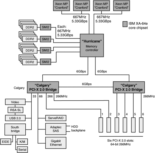
- Two Calgary PCI-X 2.0 bridges—The PCI bridge chips are connected to the Hurricane memory and I/O controller. Typically, one PCI bridge is used to interface to four of the PCI-X 2.0 slots, and the other PCI bridge is used for interfacing to two PCI-X 2.0 slots, video, USB 2.0 ports, RAID, Gigabit Ethernet, and South Bridge chips. PCI-X 2.0 slots run at speeds up to 266MHz.
Figure 3.31 shows the major components of the XA-64e chipset in a four-way configuration.
Hewlett-Packard Server Chipsets for Intel Processors
In addition to using server chipsets from third-party vendors, Hewlett-Packard has developed two distinct lines of chipsets for its servers:
- The F8 (an improved version of the Corollary/Compaq Profusion chipset) supports Xeon MP processors.
- The zx1 is the first of a line of chipsets that support PA-RISC or Itanium-family–equipped Hewlett-Packard servers in the Superdome (originally Half Dome) family.
The following sections discuss the major features of these chipsets.
The F8 Chipset for Xeon MP
The Hewlett-Packard F8 chipset was developed by Compaq as a follow-on to the eight-way Corollary chipset co-developed by Corollary and Compaq. Hewlett-Packard obtained the F8 chipset as part of its merger with Compaq. The F8 chipset is used in the Hewlett-Packard ProLinea DL740 and DL760-series eight-way servers.
The F8 chipset's major features include the following:
- Support for eight Xeon MP processors
- Dual-channel memory supporting PC133 SDRAM
- Support for PCI and PCI-X expansion slots
- Hot-plug RAID memory
- Up to 64GB of addressable memory
The F8 chipset has the following major components:
- Five F8 dual memory controllers—Four are used for data and one is used to store parity information. Each is connected to a memory cartridge containing up to eight DIMMs of dual-channel PC133 SDRAM using cache-line interleaving for better performance. Memory can be hot-plugged (in or out) without shutting down the server, and the memory controllers can correct single-bit and double-bit memory errors as well as correct DIMM failures.
- One F8 crossbar switch—The crossbar switch handles traffic running at 400 megatransfers per second between the memory controllers, processors, and the PCI bridges. It uses multiple buffers and 128 cache lines to manage eight-way traffic.
- One F8 cache coherence filter—A cache coherence filter connected to the crossbar switch prevents unnecessary traffic between L2 caches in different processors.
- Up to four PCI-X bridges with PCI hot-plug controllers—Each bridge supports two 64-bit PCI-X bus segments, and each segment can be configure to run in 33/66MHz PCI mode or 66/100MHz PCI-X mode.
Figure 3.32 illustrates the major components of the F8 chipset.
Figure 3.32 The F8 chipset supports eight-way Xeon MP processors.
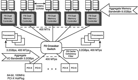
The zx1 Chipset for Itanium 2 McKinley
The Hewlett-Packard zx1 Pluto chipset for the Itanium 2 processor uses only two or three chips, making it the simplest chipset available for the Itanium 2 processor. However, although the zx1 is designed to work in one-way and two-way workstation configurations as well as in two-way and four-way server applications, it does not support eight-way implementations.
Note
The Hewlett-Packard zx1 also supports some PA-RISC processors made by Hewlett-Packard. In fact, some Hewlett-Packard servers can be converted from one processor type to the other.
The Hewlett-Packard zx1 chipset has the following components in two-way configurations:
- Hewlett-Packard chipset and memory I/O controller—This chip connects memory and processors to each other. This is designed for DDR SDRAM memory, unlike the E8870, which uses translator hubs.
- Hewlett-Packard chipset I/O adapter—This chip can be used as a bridge to an AGP 4x slot for workstation uses, PCI-X slots up to 133MHz, and for various types of I/O, including ATA/IDE, USB, SCSI, and networking.
When used in a four-way server implementation, two Hewlett-Packard zx1 scalable memory adapter chips are added to the chipset to connect the greater number of memory banks supported, and additional Hewlett-Packard Chipset I/O adapters are used to support additional 66MHz PCI-X devices. Some of Hewlett-Packard's latest servers based on the zx1 incorporate two Itanium 2 processors in the mx2 dual processor module, enabling the chipset to support eight-way implementations.
Figure 3.33 illustrates a typical two-way (workstation/server) implementation of the zx1 chipset, and Figure 3.34 shows a typical four-way server implementation.
Figure 3.33 The Hewlett-Packard zx1 chipset, shown here in a two-way configuration, uses two or three chips, depending upon the number of processors supported.
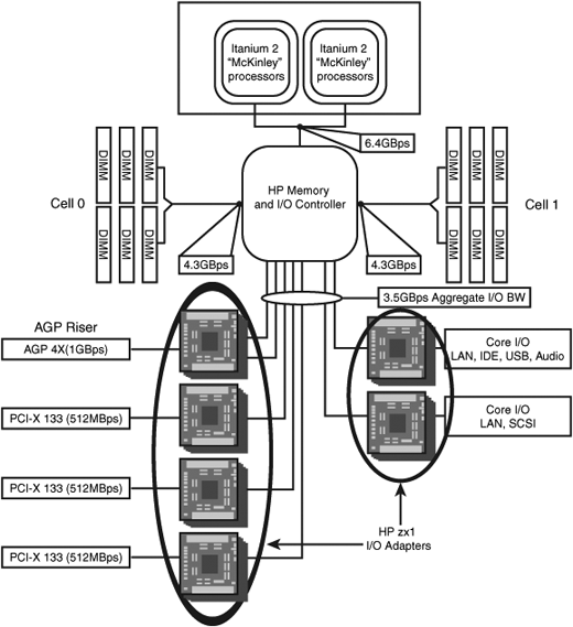
Figure 3.34 A four-way configuration of the Hewlett-Packard zx1 chipset.
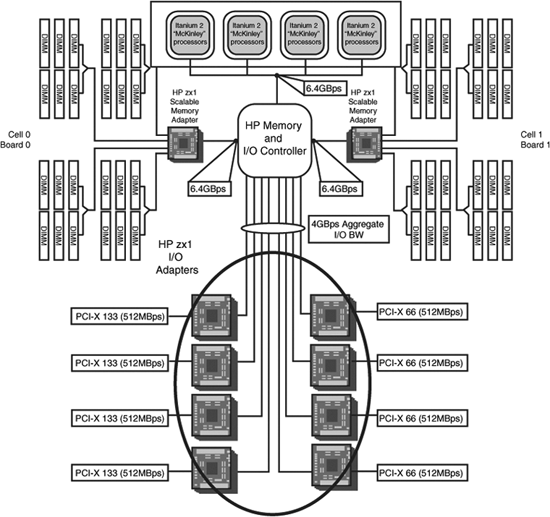
The sx1000 Pinnacles Chipset
The Hewlett-Packard Super-Scalable Processor chipset sx1000, codenamed Pinnacles, supports eight-way or higher implementations. Like the zx1, it can use single- or dual-processor cartridges. However, compared to other Itanium 2 chipsets, it has several distinct features:
- The sx1000 uses a cell architecture: Each cell comprises a cell controller chip and eight memory buffer chips. Each cell can contain four CPU modules and up to 32 PC133 registered SDRAM modules. The cell controller chip connects directly to the PCI-X system bus adapter, which connects to PCI-X bridge chips. See Figure 3.35.
Figure 3.35 The block diagram of a cell board from a Hewlett-Packard sx1000 chipset.
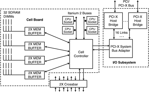
- sx1000-based servers include 2, 4, 8, or 16 cells. (Each cell includes four or eight processors, depending on whether single- or dual-processor cartridges are used; see Figure 3.36.)
Figure 3.36 The block diagram of an mx2 processor cartridge.
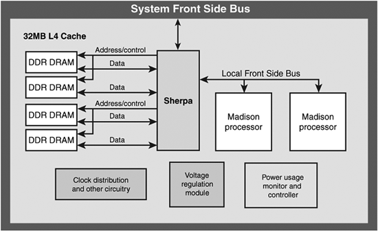
- When four or more cells are connected together, one or more crossbar switches are used. One crossbar switch is used for each group of four cells (16 processor sockets). For example, in a 64-socket system, four crossbar switches would be used.
Note
Hewlett-Packard uses the term cell to refer to a component that contains processors, control chips, and memory modules in an easily swappable package. The cell architecture design used by servers such as the sx1000 permits the server to be upgraded from a RISC-based processor such as the PA-8700 to the Intel Itanium 2 by swapping cells.
Figure 3.35 illustrates the block diagram of a four-way or eight-way sx1000 cell board. A four-way cell board uses four standard Itanium 2 processors, while an eight-way cell board uses four Hewlett-Packard mx2 processor cartridges, each of which contains two Itanium 2 processors along with 32MB L4 memory cache.
Figure 3.36 illustrates the block diagram of an mx2 processor cartridge.
The sx1000 is designed to be highly scalable to handle server tasks of virtually any size and complexity.
AMD Athlon MP and Opteron Server-Class Chipsets
The original AMD Athlon Slot A processor was not commonly used in servers for two reasons:
- It was never certified for SMP (dual-processor) operation
- There were no dual-processor chipsets that supported the processor.
However, after the Athlon design was shifted to Socket 462 (also known as Socket A), AMD developed an SMP-compatible version of the processor known as the Athlon MP. This processor was supported by AMD's AMD-760MP chipset, which was the first major chipset on the market to support DDR SDRAM memory.
However, development of server-class chipsets for AMD processors didn't become widespread until the development of the AMD Opteron, the first 64-bit processor capable of also running existing 32-bit IA-32 applications at full speed. Both AMD and third-party chipmakers have developed a number of chipsets for the Opteron. Unlike the most powerful chipsets made for Intel processors, which are almost always limited to preconfigured servers from major vendors, motherboards built for Opteron processors are widely available for "build-your-own" server builders.
The following sections discuss the various server-class chipsets available for AMD processors in greater detail.
The AMD-760 Family of Chipsets
The AMD-760 chipset, introduced in October 2000, is notable as the first chipset to support DDR SDRAM memory. The AMD-760 chipset consists of the AMD-761 system controller (North Bridge) in a 569-pin plastic ball-grid array (PBGA) package and the AMD-766 peripheral bus controller (South Bridge) in a 272-pin PBGA package.
The AMD-761 North Bridge features the AMD Athlon system bus, DDR-SDRAM system memory controller with support for either PC1600 or PC2100 memory, AGP 4x controller, and PCI bus controller. The 761 allows for 200MHz or 266MHz processor bus operation and supports the newer Athlon chips that use the 266MHz processor bus (also called the FSB).
The AMD-766 South Bridge includes a USB controller, dual UDMA/100 ATA/IDE interfaces, and the LPC bus for interfacing newer Super I/O and ROM BIOS components.
The AMD-760 chipset includes the following features:
- AMD Athlon 200/266MHz processor bus
- Dual-processor support
- PCI 2.2 bus with up to six masters
- AGP 2.0 interface that supports 4x mode
- PC1600 or PC2100 DDR SDRAM with ECC
- Support for a maximum of 2GB buffered or 4GB registered DDR SDRAM
- ACPI power management
- ATA-100 support
- USB controller
- LPC bus for Super I/O support
The AMD-760MP chipset, which uses the AMD-762 North Bridge chip, is a development of the basic AMD-760 design that supports dual-processor Athlon MP systems. It differs from the standard 760 chipset in the following ways:
- Supports dual AMD Athlon MP processors with 200/266MHz processor bus speeds
- Supports up to 4GB PC2100 DDR (registered modules)
- Supports 33MHz PCI slots in 32-bit and 64-bit widths
The AMD-760MPX chipset uses the same AMD-762 North Bridge chip as the AMD-760MP to support multiple Athlon MP processors, but it uses the AMD-768 peripheral bus controller (South Bridge) chip. It differs from the 760MP chipset in the following ways:
- The AMD-762 North Bridge chip is used to support two 66MHz 32/64-bit PCI slots.
- The AMD-768 South Bridge chip is used to support 33MHz/32-bit PCI slots.
The 760MPX chipset is a better choice for a server because of its support for 66MHz and 64-bit PCI slots, whereas the 760MP is a suitable choice for a workstation.
Figure 3.37 illustrates the 760MPX's architecture.
Figure 3.37 AMD-760MPX chipset block diagram.
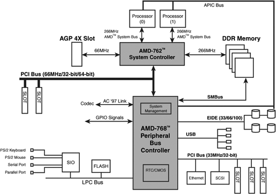
The 760MP and 760MPX chipsets continue to be popular choices for AMD-based workstations and servers that use the Athlon MP processor.
AMD Opteron Chipsets
The AMD Opteron is unique among x86-compatible server processors in having an integrated memory controller. Servers based on the Opteron can be scaled from single-processor to eight-way servers without ever needing any type of specialized memory controller or cache coherence controller. The integrated memory controller in the Opteron supports registered DDR memory, including ECC memory. By integrating the memory controller in the processor, AMD has made it possible for chipset vendors to produce simpler chipsets for Opteron than for earlier AMD-based or Intel-based servers.
The Opteron also features a HyperTransport bus between components. HyperTransport is a high-speed point-to-point interface somewhat similar to the Intel Hub Architecture discussed earlier in this chapter.
![]() See "HyperTransport," p. 155.
See "HyperTransport," p. 155.
Because the Opteron contains integrated memory controllers, it's possible to build a server that contains only an ICH (South Bridge) chip in its chipset. Also, the use of HyperTransport interconnects enables chips from different vendors to be combined in a variety of ways to create a specific motherboard design. Therefore, Table 3.21 is broken down into chipset component categories. For additional details, see the sections that follow Table 3.21.
Table 3.21 Chipset Logic for Opteron Server Platforms
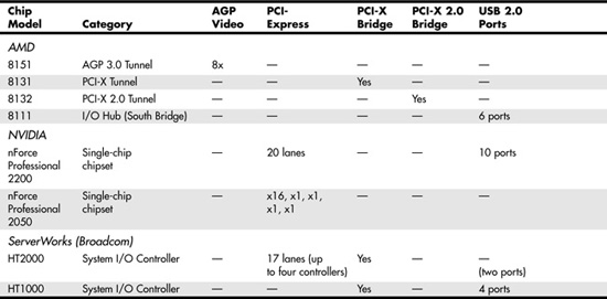
An Opteron-based system can combine various brands of chips together into a customized solution. For example, a server can use the NVIDIA nForce Professional 2200 along with an AMD 8131 or 8132 PCI-X bridge to support PCI-Express, PCI-X, and PCI cards.
Depending upon the features of a system I/O controller, it can be used by itself to create a motherboard. For example, the nForce Professional 2200, the AMD 8111, or the ServerWorks HT1000 can be used to provide disk, legacy ports, and PCI support.
This ability to mix and match chipset products from various vendors is not exactly new. Vendors such as ULi (formerly Acer Labs) have long produced South Bridge chips compatible with various vendors' North Bridge chips. However, because of the combination of a common industry standard (HyperTransport) for chip interconnects and the location of the memory controllers in the Opteron processors, Opteron-based systems provide unparalleled flexibility in motherboard chipset design. The AMD-8000, nForce Professional, and ServerWorks HT-2000/HT-1000 chipsets are all popular choices for Opteron-based servers and server motherboards.
The AMD 8000 Chipset
The AMD 8000 is AMD's first chipset designed for the Athlon 64 and Opteron families. Its architecture is substantially different from the North Bridge/South Bridge or hub-based architectures we are familiar with from the chipsets designed to support Pentium II/III/4/Celeron and AMD Athlon/Athlon XP/Duron processors.
The AMD-8000 chipset is sometimes referred to as the AMD-8151 because the AMD-8151 provides the connection between the Athlon 64 or Opteron processor and the AGP video slot, the task normally performed by the North Bridge or MCH hub in other chipsets. The name of the North Bridge or MCH hub chip is usually applied to the chipset. However, AMD refers to the AMD-8151 chip as the AGP Graphics tunnel chip because its only task is to provide a high-speed connection to the AGP slot on the motherboard. Consequently, the AMD-8151 is usually not used on Opteron motherboards used for servers. The other components of the AMD-8000 chipset include the AMD-8111 HyperTransport I/O hub (South Bridge), the AMD-8131 PCI-X tunnel chip, and the AMD-8132 PCI-X 2.0 tunnel chip.
The AMD-8151 AGP Graphics tunnel chip has the following major features:
- Support for AGP 2.0/3.0 (AGP 1x–8x) graphics cards
- 16-bit up/down HyperTransport connection to the processor
- 8-bit up/down HyperTransport connection to downstream chips
The AMD-8111 HyperTransport I/O hub (South Bridge) chip's major features include the following:
- PCI 2.2–compliant PCI bus (32-bit, 33MHz) for up to eight devices
- AC '97 2.2 audio (six-channel)
- Six USB 1.1/2.0 ports (three controllers)
- Two ATA/IDE host adapters supporting up to ATA-133 speeds
- RTC
- LPC bus
- Integrated 10/100 Ethernet
- 8-bit up/down HyperTransport connection to upstream chips
The AMD-8131 HyperTransport PCI-X tunnel chip's major features include the following:
- Two PCI-X bridges (A & B) supporting up to five PCI bus masters each
- PCI-X transfer rates up to 133MHz
- PCI 2.2 33MHz and 66MHz transfer rates
- Independent operational modes and transfer rates for each bridge
- 8-bit up/down HyperTransport connection to upstream and downstream chips
The newest member of the AMD 8000 chipset family, the AMD-8132 PCI-X 2.0 tunnel chip, offers PCI-X 2.0 transfer rates up to 266MHz. Other features are similar to those of the AMD-8131.
Figure 3.38 shows the architecture of the AMD 8000 chipset in a typical two-way server implementation.
Figure 3.38 Block diagram of the AMD 8000 chipset in a typical server implementation.
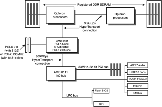
The NVIDIA nForce Professional 2000 Series of Chipsets
NVIDIA is no stranger to the AMD Opteron and AMD Athlon 64 processors: Its nForce 3–series chipsets for the AMD Athlon 64 are among the most popular and best-performing chipsets available. However, NVIDIA did not release its first chipsets optimized for Opteron-based servers, the nForce Professional 2000 series, until January 2005.
Like other recent nForce chipsets, the nForce Professional chipsets feature a highly integrated single-chip design. The initial offerings include the following:
- nForce Professional 2200
- nForce Professional 2050
Both chipsets feature the following:
- HyperTransport connections to Opteron processors and other components
- PCI-Express
- SATA RAID 0, 1, and 0+1
- Native Gigabit Ethernet with hardware firewall
- Support for up to eight-way or higher implementations
- Support for dual-core Opteron processors
- Second-generation SATA (3GBps)
The 2200 also features support for up to 10 USB 2.0 ports, 20 flexible PCI-Express lanes, 8-channel AC '97 audio, ATA-133, and a 33MHz, 32-bit PCI interface. The 2200's implementation of RAID can include both SATA and ATA/IDE drives in the same array. The 2050 lacks USB, PCI, and ATA-133 support; supports an x16 PCI-Express slot and four x1 slots; and does not have onboard audio.
Although neither the 2200 nor 2050 chipsets support PCI-X slots natively, they support connections to other Opteron-compatible chipset components via HyperTransport. As a result, some vendors have combined the AMD 8131 or 8132 chips with the 2200 or 2050 chips to produce systems with PCI-X support.
The ServerWorks HT Series of Chipsets
Broadcom's ServerWorks division released its first logic chips for Opteron systems, the HT-2000 and HT-1000, in April 2005. The HT-2000 I/O controller combines support for two PCI-X slots or integrated devices, a two-port Gigabit Ethernet controller, and 17-lane PCI-Express support (with up to four PCIe controllers) in a single chip. The HT-2000 provides 16x HyperTransport upstream connections at up to 2GHz to the host and 8x HyperTransport downstream connections at up to 1.6GHz to the HT-1000 I/O controller or other chips. A single HT-2000 chip supports up to two Opteron processors. A four-way platform uses two HT-2000 chips, and an eight-way platform uses four HT-2000 chips. With any number of HT-2000, a single HT-1000 I/O controller is used to provide support for other components.
The companion HT-1000 controller supports two PCI-X slots, as well as 32-bit PCI slots; USB 2.0 ports; one ATA/IDE and up to four SATA drives; SATA RAID levels 0, 1, 0+1, and 5; and an LPC bus. Because of its versatile design, the HT-1000 I/O controller can also be used by itself for entry-level two-way servers, providing an 8x HyperTransport connection to the host.
Figure 3.39 illustrates an advanced two-way configuration using the HT-2000 and HT-1000 and a basic two-way configuration using the HT-1000 by itself.
Figure 3.39 Block diagram of the ServerWorks HT-2000/HT-1000 chipset in typical advanced (left) and basic (right) two-way server implementations.
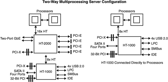
Determining Hardware Compatibility with Server Platforms
Before you purchase or build a new server or upgrade an existing server, it's very important that you determine whether the server is compatible with both of the following:
- The onboard or external hardware you need to use with that server
- The operating system you are using (or intend to use) with that server
The following sections describe how you can best determine this information.
Determining Operating System Compatibility
If you are buying a new server or building one from scratch (a very real possibility today, especially if you want to create a single-processor to four-way server), you need to verify the compatibility of your server or server motherboard with the operating system you plan to use with it.
If you are purchasing an already-built server, this is relatively simple. Server vendors usually offer a variety of preconfigured systems that include validated operating systems. However, if you are planning to build your own server from scratch or by upgrading an existing system, you need to be more careful. The following sections describe methods and resources you can use to determine that your hardware is ready to run the server operating system of your choice.
![]() See "Server NOSs," p. 758.
See "Server NOSs," p. 758.
Determining Windows Compatibility
Windows Server 2003 is the "king of the hill" in server operating systems today. Most vendors of server-class hardware from motherboards to PCI-X cards list Windows Server 2003 compatibility on their websites. You can also verify compatibility for specific hardware with the Windows Server Catalog. You can click the link available at the "Products Designed for Microsoft Windows—Windows Catalog and HCL" page at www.microsoft.com/whdc/hcl/default.mspx to check compatibility with Windows Server 2003 and Windows 2000 Server.
If you need drivers for existing hardware, you should make sure you understand what version of Windows Server 2003 you need drivers for:
- The standard 32-bit versions of Windows Server 2003 use the same drivers as Windows XP Professional.
- The x64 edition designed for Intel EM64T and AMD Opteron processors requires specially written 64-bit drivers.
- Itanium 2–based servers use the 64-bit edition of Windows Server 2003; this uses different 64-bit drivers than the x64 edition.
Determining Linux Compatibility
Many hardware vendors now provide drivers for various versions or distributions of Linux on their websites. However, you should first visit the Linux distribution vendor's website to consult the latest catalog of certified and compatible hardware.
In some cases, you might need to use an open-source driver for certain hardware. You should be sure to note where the driver came from and check for updates.
Determining Sun Solaris Compatibility
Sun maintains a list of compatible hardware for Sun Solaris 9 and 10 on its website. You can search the Sun Solaris hardware compatibility list at www.microsoft.com/whdc/hcl/default.mspx.
If you need a driver for a particular device, you should follow the link provided. The compatibility notes list any problems with the driver.
Integration with Bus Types
Generally, current server operating systems can be used with the most common bus types on the market, including PCI, USB, PCI-X, PCI-Express, and AGP. As with any other computer hardware item, driver support is necessary before a particular bus or component will work.
If you are coming from a desktop computer background, you have probably noticed that some server chipsets use older ICH or South Bridge chips than their desktop counterparts and that many of them use older and slower memory types than those found in the latest desktop computers. The most likely reason for this is to assure stability. Although desktop users can accept a certain amount of instability in return for better performance, servers must be stable, even if it means using "last year's" chipset component.
Conclusions, Troubleshooting, and Documentation
Choosing the right server platform for your project is essential to achieving a server solution that will be satisfactory today and will be able to grow with your needs. Here are some methods that will help you avoid problems and diagnose them when they appear:
- Gather system and chipset-specific documentation for your platform. You can find countless pages of documentation from chipset and system vendors, most of it available online in HTML or PDF format. You should download as much of this information as possible and order anything not available electronically in paper or CD-ROM format.
- Familiarize yourself with the features and limitations of your server platform. The chipset is the server! If the chipset isn't designed to work with a particular type of memory or with a particular processor type, you must do without that particular change or consider an upgrade.
- Use the troubleshooting and technical resources provided by the operating system and hardware vendors. Some vendors provide downloadable programs that can be used to check compatibility or perform tests on components.
- Keep your information up-to-date. Don't forget to download specification updates for your system and chipset.
- If you use a search engine to locate solutions, there are a couple ways you can save your information for easier access. You can use the Save as PDF option in Adobe Acrobat 5.0 or greater to create a PDF (Acrobat Reader) version of a web page. With Internet Explorer, you can choose Save as Web Archive to save all the contents of a web page in a single file.