
Appendix
Chart 1. DC–DC Design Chart
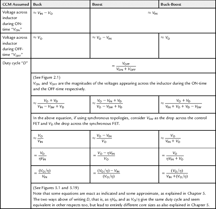
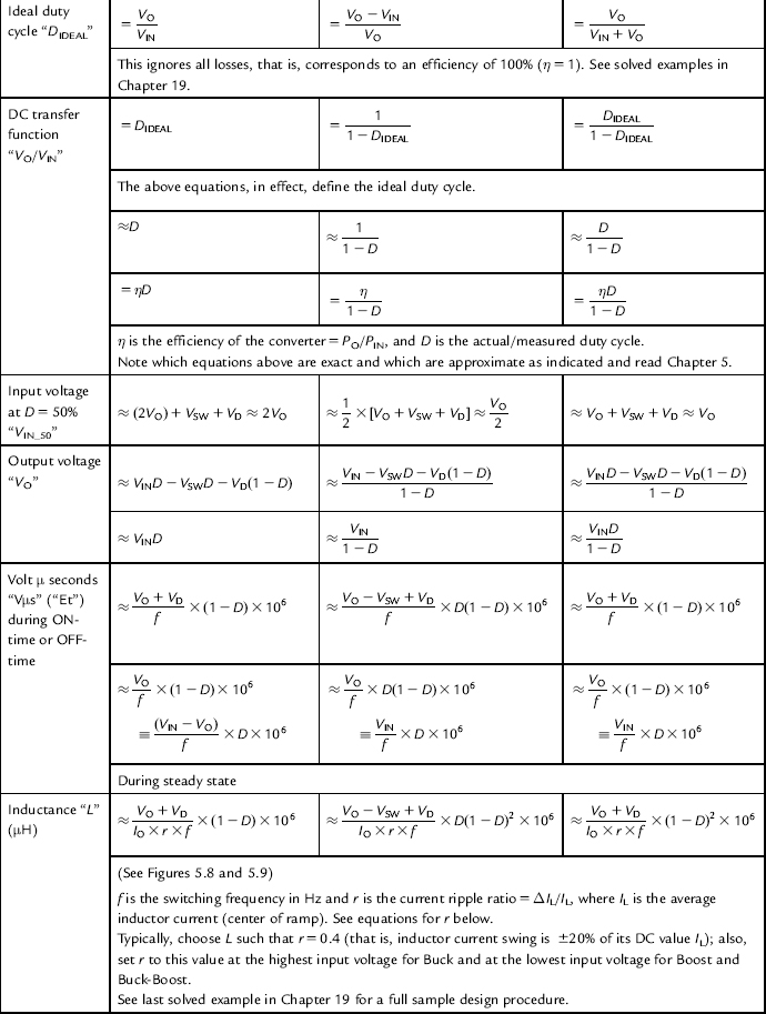
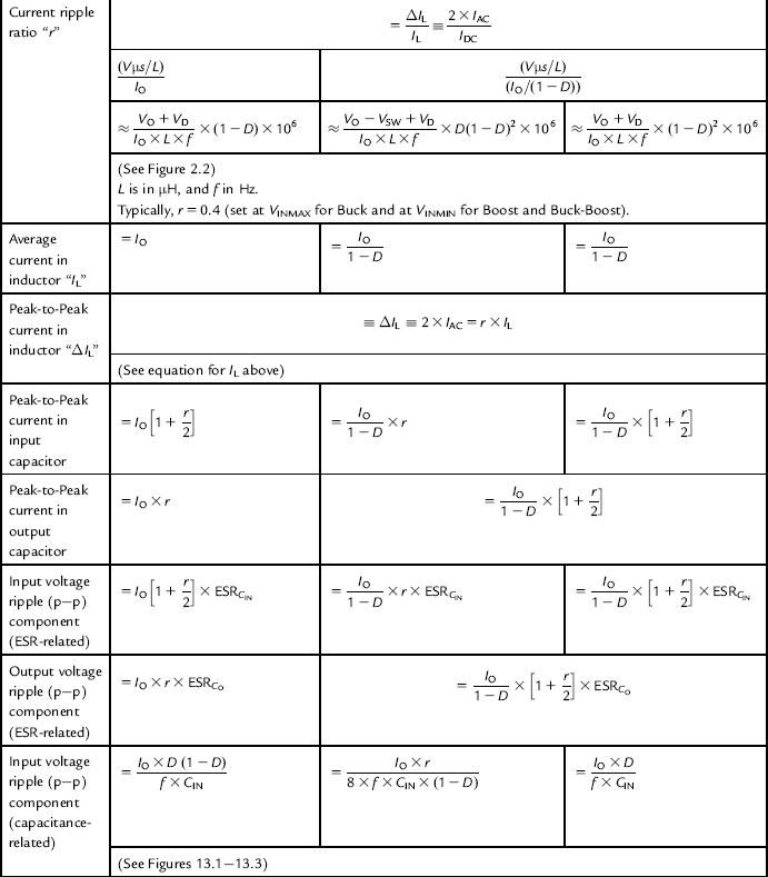
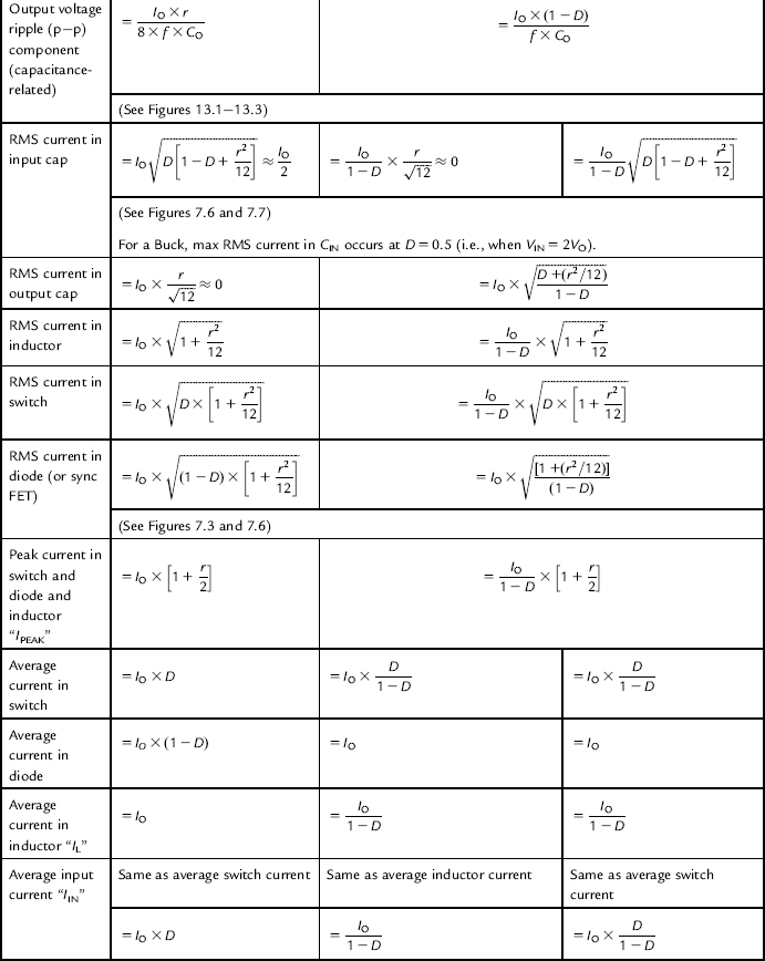
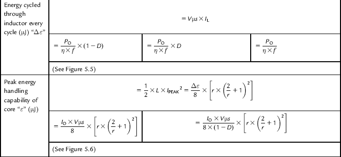
Chart 2. AC–DC Design Chart
| CCM Assumed | Single-Ended Forward (like a Buck) | Flyback (like a Buck-Boost) |
| Transformer turns ratio “n” | ||
| Reflected output voltage “VOR” | ||
| Reflected input voltage “VINR” | ||
| Reflected output current “IOR” | ||
| Reflected input current “IINR” | ||
| (See Figure 3.2) See also, the equation for IIN further below | ||
| Duty cycle | ||
| (See Figure 5.1) | ||
| Ideal duty cycle “DIDEAL” | ||
| DC transfer function “VO/VIN” | ||
| η is the efficiency of the converter=PO/PIN, D is the actual/measured duty cycle , and n is the turns ratio. | ||
| Inductance “L” (μH) | ||
| (See Figures 5.8, 5.9, and 14.4) This refers to the inductance of the output choke of a Forward converter and the Primary side of the transformer in a flyback (measured with the Secondary windings open). f is the switching frequency in Hz, and r is the current ripple ratio; see below. Typically, choose L such that r=0.4 (i.e., inductor current swing is ±20% of its DC or center of ramp value IL); also, set r to this value at the highest input voltage for Forward and at the lowest input voltage for flyback. | ||
| Average current in inductor “IL” (or center of ramp) | Primary side: | |
| Secondary side: | ||
| (See Figure 3.2) | ||
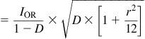
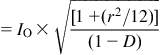
| Current ripple ratio “r” | ||
| (See Figures 2.2 and 3.2) r is the current ripple ratio=ΔIL/IL≡2×IAC/IDC, where IL is the average inductor current (the center of ramp, i.e., IDC) and IAC is its AC component≡ΔIL/2; L is in μH and f is in Hz.Typically, set r=0.4, that is, inductor current swing is then ±20% of its DC (center of ramp) value “IL.” For a flyback, r is the same on either side of the transformer, though currents and current swings on either side of the transformer are scaled as per the turns ratio. | ||
| Peak-to-Peak current in inductor “ΔIL” | ||
| (See equations for IL above) | ||
| Peak-to-Peak current in input capacitor | ||
| Ignoring transformer magnetization current | ||
| Peak-to-Peak current in output capacitor | ||
| Input voltage ripple (p–p) component (ESR-related) | ||
| Ignoring transformer magnetization current | ||
| Output voltage ripple (p–p) component (ESR-related) | ||
| Input voltage ripple (p–p) component (capacitance-related) | ||
| Ignoring transformer magnetization current | ||
| (See Figures 13.1–13.3) | ||
| Output voltage ripple (p–p) component (capacitance-related) | ||
| (See Figures 13.1–13.3) | ||
| RMS current in input cap |  |
 |
| Ignoring transformer magnetization current | ||
| (See Figures 7.6 and 7.7) For a Forward converter, max RMS current in CIN occurs at D=0.5, that is, at which VIN/η=2×VO. | ||
| RMS current in output cap | ||
| RMS current in inductor and windings | Primary side: |
Primary side: |
| Ignoring transformer magnetization current | ||
Secondary side: |
Secondary side: | |
| Output choke: | ||
| (See Figure 7.3) | ||
| RMS current in switch |  |
 |
| Ignoring transformer magnetization current | ||
| RMS current in diode (or sync FET) | Output diode (to transformer):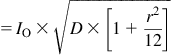 |
 |
Freewheeling diode (to ground):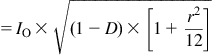 | ||
| (See Figures 7.3 and 7.6) | ||
| Average current in switch | ||
| Ignoring transformer magnetization current | ||
| Average current in diode | Output diode (to transformer): |
|
| Freewheeling diode (to ground): | ||
| Average input current “IIN” | Same as average switch current | |
| Peak energy handling capability of core “ε” (μJ) | 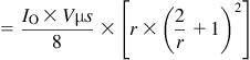 |
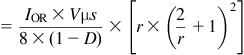 |
| (See Figures 5.5 and 5.6) This peak energy refers to the output choke of a Forward converter and to the transformer of a flyback. For flyback, use the Vμs appearing across the Primary winding, that is, VIN × D/f × 106 or equivalently VOR×(1−D)/f ×106. | ||
Chart 3. Multi-topology Voltage Stresses Design Chart
|
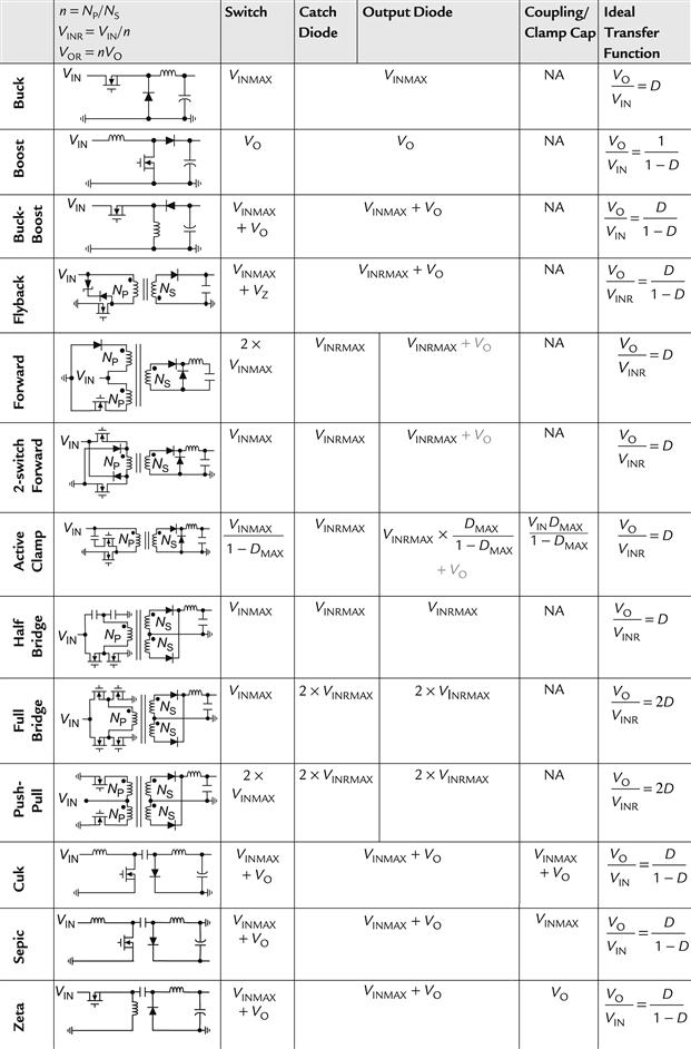
See additional comments in Table 7.1.
..................Content has been hidden....................
You can't read the all page of ebook, please click here login for view all page.