Chapter 3
Overview of Embedded Systems Development Lifecycle Using DSP
Chapter Outline
The embedded system lifecycle using DSP
Step 1 – Examine the overall needs of the system
Step 2 – Select the hardware components required for the system
A general signal processing solution
Embedded systems
As we have seen in Chapter 2, an embedded system is a specialized computer system that is integrated as part of a larger system. Many embedded systems are implemented using digital signal processors (DSPs). The DSP will interface with the other embedded components to perform a specific function. The specific embedded application will determine the corresponding DSP to be used. For example, if the embedded application is one that performs video processing, the system designer may choose a DSP that is customized to perform media processing including video and audio processing. This device contains dual channel video ports that are software configurable for input or output, as well as video filtering and automatic horizontal scaling and support of various digital TV formats such as HDTV, multi-channel audio serial ports, multiple stereo lines, and an ethernet peripheral to connect to IP packet networks. It is obvious that the choice of DSP system depends on the embedded application.
In this chapter we will discuss the basic steps involved in developing an embedded application using DSP.
The embedded system lifecycle using DSP
In this section we will give an overview of the general embedded system lifecycle using DSP. There are many steps involved in developing an embedded system – some are similar to other system development activities and some are unique. We will step through the basic process of embedded system development focusing on DSP applications.
Step 1 – Examine the overall needs of the system
Comparing and choosing a design solution is a difficult process. Often the choice comes down to emotion or attachment to a particular vendor or processor, or to inertia based on prior choosing and comfort level. The embedded designer must take a positive logical approach to comparing solutions, based on well-defined selection criteria. For DSP, there is a set of specific selection criteria that must be discussed. Many signal processing applications will require a mix of several system components in the overall design solution including:
What is a DSP solution?
A typical DSP product design uses the is digital signal processor itself, analog/mixed signal functions, memory, and software; all is designed with a deep understanding of overall system function. In the product, the analog signals of the real world, signals representing anything from temperature to sound or images, are translated into digital bits – zeros and ones – by an analog/mixed signal device. Then the digital bits or signals are processed by the DSP. Digital signal processing is much faster and more precise than traditional analog processing. This type of processing speed is needed for today’s advanced communications devices where information requires instantaneous processing, and in many portable applications that are connected to the internet.
There are many selection criteria for embedded DSP systems. These include, but are not limited to:
These are the major selection criteria defined by Berkeley Design Technology Incorporated (bdti.com). Other selection criteria may be ‘ease of use’ which is closely linked to ‘time to market’ and also ‘features.’ Some of the basic rules to consider in this phase are:
Step 2 – Select the hardware components required for the system
In many systems, a general purpose processor (GPP), field programmable gate array (FPGA), microcontroller (uC), or DSP is not used as a single-point solution. This is because designers often combine solutions, maximizing the strengths of each device (Figure 3-1).
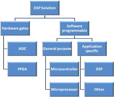
Figure 3-1: Many applications, multiple solutions.
One of the first decisions that designers often make when choosing a processor is whether they would like a software programmable processor in which functional blocks are developed in software using C or assembly, or a hardware processor in which functional blocks are laid out logically in gates. Both FPGAs and application specific integrated circuits (ASICs) may integrate a processor core (very common in ASICs).
Hardware gates
Hardware gates are logical blocks laid out in a flow; therefore any degree of parallelization of instructions is theoretically possible. Logical blocks have very low latency, and therefore FPGAs are more efficient for building peripherals than ‘bit-banging’ using a software device.
If a designer chooses to design in hardware, he or she may design using either FPGA or ASIC. FPGAs are termed ‘field programmable’ because their logical architecture is stored in a non-volatile memory and booted into the device. Thus FPGAs may be reprogrammed in the field simply by modifying the non-volatile memory (usually FLASH or EEPROM). ASICs are not field programmable. They are programmed at the factory using a mask which cannot be changed. ASICs are often less expensive and/or lower power. They often have sizable non-recurring engineering (NRE) costs.
Software programmable
In this model, instructions are executed from memory in a serial fashion (i.e. one per cycle). Software programmable solutions have limited parallelization of instructions. However, some devices can execute multiple instructions in parallel in a single cycle. Because instructions are executed from memory in the CPU, device functions can be changed without having to reset the device. Also, because instructions are executed from memory, many different functions or routines may be integrated into a program without the need to lay out each individual routine in gates. This may make a software programmable device more cost effective for implementing very complex programs with a large number of subroutines.
If a designer chooses to design in software, there are many types of processors available to choose from. There are a number of general purpose processors but, in addition, there are processors that have been optimized for specific applications. Examples of such application-specific processors are graphics processors, network processors, and digital signal processors (DSPs). Application-specific processors usually offer higher performance for a target application, but are less flexible than general purpose processors.
General purpose processors
Within the category of general purpose processors (GPPs) are microcontrollers (uC) and microprocessors (uP) (see Figure 3-2).
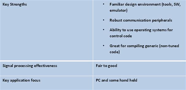
Figure 3-2: General purpose processor solutions.
Microcontrollers usually have control-oriented peripherals. They are usually lower cost and lower performance than microprocessors. Microprocessors usually have communications-oriented peripherals. They are usually higher cost and higher performance than microcontrollers.
Note that some GPPs have integrated MAC units. It is not particularly a strength of GPPs to have this capability, because all DSPs have MACs, but it is worth noting because a student might mention it. Regarding performance of the GPP’s MAC, it is different for each one.
Microcontrollers
A microcontroller is a highly integrated chip that contains many or all of the components comprising a controller. This includes a CPU, RAM and ROM, I/O ports, and timers. Many general-purpose computers are designed the same way. But a microcontroller is usually designed for very specific tasks in embedded systems. As the name implies, the specific task is to control a particular system, hence the name microcontroller. Because of this customized task, the device parts can be simplified, which makes these devices very cost effective solutions for these types of applications (see Figure 3-3).
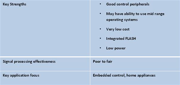
Figure 3-3: Microcontroller solutions.
Some microcontrollers can actually do a multiply and accumulate (MAC) in a single cycle. But that does not necessarily make it DSP-centric. True DSP can allow two 16 × 16 MACs in a single cycle, including bringing the data in over the busses. It is this that truly makes the application a DSP. So, devices with hardware MACs might get a ‘fair’ rating. Others get a ‘poor’ rating. In general, microcontrollers can do DSP but they will generally do it slower.
FPGA solutions
An FPGA is an array of logic gates that are hardware-programmed to perform a user-specified task. FPGAs are arrays of programmable logic cells interconnected by a matrix of wires and programmable switches. Each cell in an FPGA performs a simple logic function. These logic functions are defined by an engineer’s program. FPGAs contain large numbers of these cells (1000–100,000) available to use as building blocks in DSP applications. The advantage of using FPGAs is that the engineer can create special purpose functional units that can perform limited tasks very efficiently. FPGAs can be reconfigured dynamically as well (usually 100–1,000 times per second, depending on the device). This makes it possible to optimize FPGAs for complex tasks at speeds higher than that which can be achieved using a general purpose processor. The ability to manipulate logic at the gate level means it is possible to construct custom DSP-centric processors that efficiently implement the desired DSP function. This is possible by simultaneously performing all of the algorithm’s subfunctions. This is where the FPGA can achieve performance gains over a programmable DSP processor.
The DSP designer must understand the trade-offs when using FPGA (see Figure 3-4). If the application can be done in a single programmable DSP, that is usually the best way to go, since talent for programming DSP is usually easier to find than FPGA designers. Also, software design tools are common, cheap, and sophisticated, which improves development time and cost. Most of the common DSP algorithms are also available in well-packaged software components. It is harder to find these same algorithms implemented and available for FPGA designs.
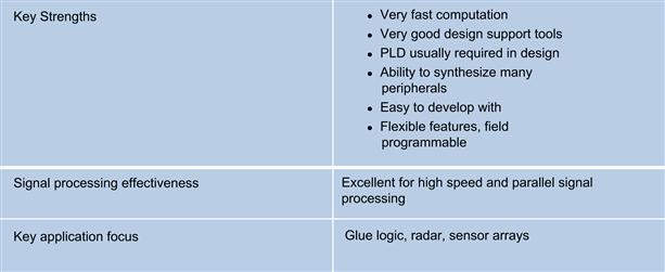
Figure 3-4: FPGA solutions for DSP.
FPGA is worth considering, however, if the desired performance cannot be achieved using one or two DSPs, or when there may be significant power concerns (although DSP is also a power efficient device – benchmarking needs to be performed), or when there may be significant programmatic issues when developing and integrating a complex software system.
Typical applications for FPGA include radar/sensor arrays, physical system and noise modeling and any high I/O and high bandwidth application.
Digital signal processors
A DSP is a specialized microprocessor used to efficiently perform calculations on digitized signals that are converted from the analog domain. One of the big advantages of DSP is the programmability of the processor, which allows important system parameters to be easily changed to accommodate the application. DSPs are optimized for digital signal manipulations.
DSPs provide ultra-fast instruction sequences, such as shift and add, and multiply and add. These instruction sequences are common in many math-intensive signal processing applications. DSPs are used in devices where this type of signal processing is important, such as sound cards, modems, cell phones, high-capacity hard disks, and digital TVs (Figure 3-5).
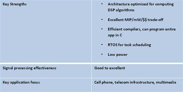
Figure 3-5: DSP processor solutions.
In reality, the choice is not that clear, as DSP functions, for example, are making their way onto microcontrollers and vice versa. The automotive segment is a good example of this. High performance power train applications for six cylinder and higher require significant signal processing. Microcontrollers are used for this purpose (see Figure 3-6).
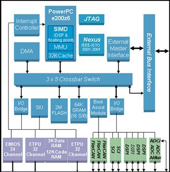
Figure 3-6: The MPC5554 is used in the automotive industry specifically addressing high performance power train applications 6 cylinder and above.
The MPC5554 in this example uses the zen 6 processor core with 32K of cache and memory management unit. It includes 2MB of Flash and 111K SRAM distributed as Data RAM, eTPU coprocessor RAM, and Cache. This microcontroller has general communications peripherals common to automotive and industrial applications such as CAN, SPI, Serial, and LIN. The MPC5554 has dual analog-to-digital converters supporting 40 channels.
This microcontroller is highly flexible and can be programmed to perform complex scatter/gather operations. But the key feature relevant to this discussion is the signal processing engine (SPE) located inside the core.
The SPE is a SIMD architecture processing engine – Single Instruction Multiple Data (see Figure 3-7). This allows multiple data elements to be acted upon by a single common operation.
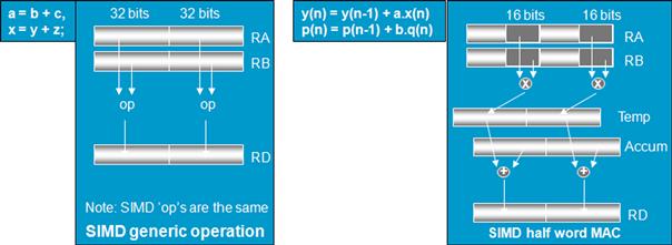
Figure 3-7: Architecture of the signal processing engine (SPE).
This improves performance on algorithms that have tight inner loops and operate on large sets of data. Signal processing algorithms are examples of this type of algorithm.
The SPE utilizes the existing components of the core to bring improved performance with minimum additional complexity of the core and easier integration with existing tools and software. From a user perspective the most visible aspect of the core with SPE APU is that the registers are shared with the basic core and extended to 64 bits.
The pipeline for instruction and data fetch are also extended to 64 bits for optimal transfer of data through the SIMD. This is essentially an arithmetic processing unit (APU) that provides signal processing capabilities aimed specifically at DSP operations, such as filters and FFTs.
SPE engines like this provide significant DSP capability, such as SIMD functionality, full set of arithmetic, logical and floating point operations, multiple Multiply and Multiply-Accumulate Instructions, 16 and 32 bit loads and stores and data movement instructions, FFT address calculation through bit-reverse increment instruction, 64-bit accumulator, etc.
SPE can be used to accelerate DSP algorithms. Let’s take a look at an FIR filter. Figure 3-8 shows a basic FIR filter. In Figure 3-9 we take a look at what a similar code set written for the SPE might look like.
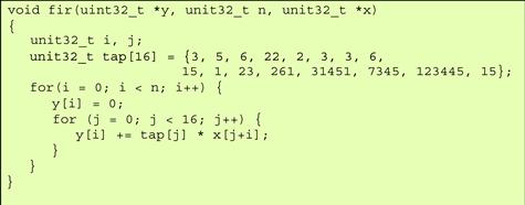
Figure 3-8: Basic FIR filter.
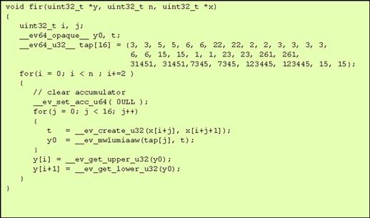
Figure 3-9: FIR filter using SPE intriniscs.
First there are a set of creation intrinsics – these intrinsics create new generic 64-bit opaque data types from the given inputs passed by value. More specifically, they are created from the following inputs:
The intrinsic ‘evmwlumiaaw’ stands for Vector, Multiply, Word, Low, Unsigned, Modulo, Integer, and Accumulate in Words.
For each word element in the accumulator, the corresponding word unsigned integer elements in rA and rB are multiplied. The least significant 32 bits of each product are added to the contents of the corresponding accumulator word and the result is placed into rD and the accumulator.
The ‘Get_Upper/Lower’ intrinsics specify whether the upper or lower 32 bits of the 64-bit opaque data type are returned. Only signed/unsigned 32-bit integers or single-precision floats are returned.
To initialize the accumulator, the ‘evmra’ instruction is used.
DSP acceleration units like SPE are used to help cost reduce applications from having to use multiple devices. Figure 3-10 shows how a custom ASIC can be removed from this engine control application by using the SPE inside the microcontroller, thus cost reducing the device. In summary, although we can assess DSP capability by discrete processor type, such as micro, DSP, ASIC, etc., many times the solution is a hybrid of several of these processing elements.
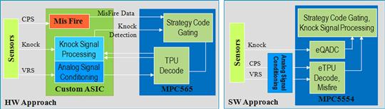
Figure 3-10: SPE are DSP capabilities inside the microcontroller that can be used to reduce the overall number of components in a DSP system.
A general signal processing solution
The solution shown in Figure 3-10 allows each device to perform the tasks that it is best at, achieving a more efficient system in terms of cost/power/performance. For example, in Figure 3-10, the system designer may put the system control software as follows: state machines and other communication software on the general purpose processor or microcontroller, the high performance, single dedicated fixed functions on the FPGA, and the high I/O signal processing functions on the DSP.
When planning the embedded product development cycle there are multiple opportunities to reduce cost and/or increase functionality using combinations of GPP/uC, FPGA, and DSP. This becomes more of an issue in higher-end DSP applications. These are applications which are computationally intensive and performance critical. These applications require more processing power and channel density than can be provided by GPPs alone. For these high-end applications there are software/hardware alternatives which the system designer must consider. Each alternative provides different degrees of performance benefits and must also be weighed against other important system parameters including cost, power consumption, and time to market.
The system designer may decide to use an FPGA in a DSP system for the following reasons:
• decision to extend the life of a generic, lower-cost microprocessor or DSP by offloading computationally intensive work to an FPGA
• decision to reduce or eliminate the need for a higher-cost, higher performance DSP processor
If the throughput of an existing system must increase to handle higher resolutions, or larger signal bandwidths, an FPGA may be an option. If the required performance increases are computational in nature, an FPGA may again be an option.
Since the computational core of many DSP algorithms can be defined using a small amount of C code, the system designer can quickly prototype new algorithmic approaches on FPGAs before committing to hardware or other production solutions like an ASIC implementing ‘glue’ logic; various processor peripherals and other random or ‘glue’ logic are often consolidated into a single FPGA. This can lead to reduced system size, complexity, and cost.
By combining the capabilities of FPGAs and DSP processors, the system designer can increase the scope of the system design solution. A combination of fixed hardware and programmable processors is a good model for enabling flexibility, programmability, and computational acceleration of hardware for the system. An example of this is shown in Figure 3-11. This multicore DSP device has six DSP cores and fixed hardware gates (accelerators) to perform specialized functions. The MAPLE accelerator performs signal processing functions like FFT and Viterbi decoding. The QUICC accelerator performs network protocol functions. The SEC accelerator performs security protocol processing.
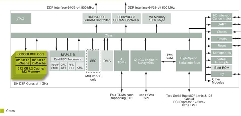
Figure 3-11: General signal processing solution.
DSP acceleration decisions
In DSP system design, there are several things to consider when determining whether a functional component should be implemented in hardware or software:
• Computational complexity; the system designer must analyze the algorithm to determine if it maps well onto the DSP architecture and programming model, or whether it maps better onto a hardware model to exploit certain forms of parallelism that cannot be found in a von Neumann or Harvard architecture of a programmable DSP.
• Signal processing algorithm parallelism; modern processor architectures have various forms of instruction level parallelism (ILP). Modern DSPs have very long instruction word (VLIW) architecture. These DSPs exploit ILP by grouping multiple instructions (adds, multiplies, loads, and stores) for execution in a single processor cycle. For DSP algorithms that map well to this type of instruction parallelism, significant performance gains can be realized. But not all signal processing algorithms exploit such forms of parallelism. Filtering algorithms such as finite impulse response (FIR) algorithms are recursive and are sub-optimal when mapped to programmable DSPs. Data recursion prevents effective parallelism and ILP. As an alternative, the system designer can build dedicated hardware engines in an FPGA.
• Computational complexity; depending on the computational complexity of the algorithms, these may run more efficiently on an FPGA instead of a DSP. It may make sense, for certain algorithmic functions, to implement in a FPGA and free up programmable DSP cycles for other algorithms. Some FPGAs have multiple clock domains built into the fabric which can be used to separate different signal processing hardware blocks into separate clock speeds based on their computational requirements. FPGAs can also provide flexibility by exploiting data and algorithm parallelism using multiple instantiations of hardware engines in the device.
• Data locality; the ability to access memory in a particular order and granularity is important. Data access takes time (clock cycles) due to architectural latency, bus contention, data alignment, direct memory access (DMA) transfer rates, and even the type of memory being used in the system. For example, static RAM (SRAM), which is very fast, but much more expensive than dynamic RAM (DRAM), is often used as cache memory due to its speed. Synchronous DRAM (SDRAM), on the other hand, is directly dependent on the clock speed of the entire system (that’s why they call it synchronous). It basically works at the same speed as the system bus. The overall performance of the system is driven in part by which type of memory is being used. The physical interfaces between the data unit and the arithmetic unit are the primary drivers of the data locality issue.
• Data parallelism; many signal processing algorithms operate on data that is highly capable of parallelism, such as many common filtering algorithms. Some of the more advanced high-performance DSPs have single instruction multiple data (SIMD) capability in the architectures and/or compilers that implement various forms of vector processing operations. FPGA devices are also good at this type of parallelism. Large amounts of RAM are used to support high bandwidth requirements. Depending on the DSP processor being used, an FPGA can be used to provide this SIMD processing capability for certain algorithms that have these characteristics.
A DSP-based embedded system could incorporate one, two or all three of these devices depending on various factors:
The trend in embedded DSP development is moving more toward programmable solutions. There will always be a trade-off, depending on the application.
‘Cost’ can mean different things to different people. Sometimes, the solution is to go with the lowest ‘device cost.’ However, if the development team then spends large amounts of time re-doing work, the project may be delayed and the ‘time to market’ window may extend, which, in the long run, costs more than the savings of the low cost device.
The first point to make is that a purely 100% software or hardware solution is usually the most expensive option. A combination of the two is the best. In the past, more functions were done in hardware and less in software. Hardware was faster, cheaper (ASICs) and good C compilers for embedded processors just weren’t available. However, today, with better compilers, and faster and lower-cost processors available, the trend is toward more of a software programmable solution. A software-only solution is not (and most likely never will be) the best overall option. Some hardware will still be required. For example, let’s say you have 10 functions to perform and two of them require extreme speed. Do you purchase a very fast processor (which costs 3–4 times the speed you need for the other 8 functions) or do you spend 1 times the price on a lower-speed processor and purchase an ASIC or FPGA to do only those two critical functions? It’s probably best to choose the combination.
Cost can be defined by a combination of the following:
A combination of software and hardware always gives the lowest cost system design.
Step 3 – Understand DSP basics and architecture
One compelling reason to choose a DSP processor for an embedded system application is performance. Three important questions to understand when deciding on a DSP are:
In this section we will begin to answer these questions. So what does make a DSP a DSP? A DSP is really just an application-specific microprocessor. They are designed to do a certain thing, signal processing, very efficiently. For example, consider the signal processor algorithms in Figure 3-12.
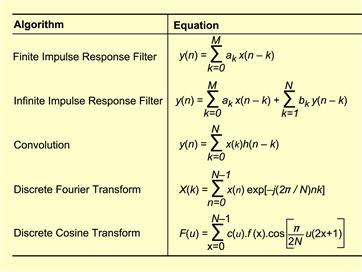
Figure 3-12: Typical DSP algorithms.
Notice the common structure of each of the algorithms:
These algorithms all share some common characteristics; they perform multiplies and adds over and over again. This is generally referred to as the sum of products (SOP).
DSP designers have developed hardware architectures that allow the efficient execution of algorithms to take advantage of this algorithmic specialty in signal processing. For example, some of the specific architectural features of DSPs accommodate the algorithmic structure described in Figure 3-13.
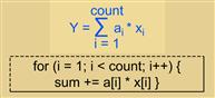
Figure 3-13: Architectural features of DSPs accommodate the algorithmic structure.
As an example, consider the FIR diagram in Figure 3-14. This is a DSP algorithm which clearly shows the multiply/accumulate and demonstrates the need for doing MACs very fast, along with reading at least two data values. As shown, the filter algorithm can be implemented using a few lines of C source code. The signal flow diagram in Figure 3-8 shows this algorithm in a more visual context. Signal flow diagrams are used to show overall logic flow, signal dependencies, and code structure. They make a nice addition to code documentation.
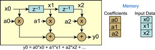
Figure 3-14: Signal flow graph for FIR filter.
To execute at top speed, a DSP needs to:
DSP architectures support the requirements above via:
• High-speed memory architectures supporting multiple accesses/cycle
• Multiple read busses allowing 2 (or more) data reads/cycle from memory
• The processor pipeline overlaying CPU operations allowing 1-cycle execution
All of these things work together to result in the highest possible performance when executing DSP algorithms.
Other DSP architectural features are summarized below:
• Circular buffers; automatically wrap pointer at end of the data or coefficient buffer
• Repeat single, and repeat block; execute next instruction or block of code with zero loop overhead
• Numerical issues; handles fixed or floating point math issues in hardware (e.g., saturation, rounding, overflow)
• Unique addressing modes; address pointers have their own ALU which is used to auto- increment and auto-decrement pointers, and create offsets with no cycle penalty
• Instruction parallelism; executes up to eight instructions in a single cycle.
Models of DSP processing
There are two types of DSP processing models, single sample model and block processing model. In a single sample model of signal processing (Figure 3-15a) the output must result before the next input sample. The goal is minimum latency (in-to-out time). These systems tend to be interrupt intensive, as interrupts drive the processing for the next sample. Example DSP applications include motor control and noise cancellation.
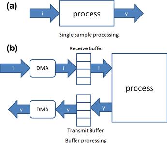
Figure 3-15: (a) Single sample and (b) block processing models of DSP.
In the block processing model (Figure 3-15b) the system will output a buffer of results before the next input buffer fills. DSP systems like this use the DMA to transfer samples to the buffer. There is increased latency in this approach as the buffers are filled before processing. However, these systems tend to be computationally efficient. The main types of DSP applications that use block processing include cellular telephony, video, and telecom infrastructure.
An example of stream processing is averaging data sample. A DSP system that must average the last three digital samples of a signal together, and output a signal at the same rate as that which is being sampled, must do the following:
These three steps must complete before the next sample is taken. This is an example of stream processing. The signal must be processed in real time. A system that is sampling at 1000 samples per second has one-thousandth of a second to complete the operation, in order to maintain real-time performance.
Block processing, on the other hand, accumulates a large number of samples at a time and processes those samples while the next buffer of samples is being collected. Algorithms such as the fast fourier transform (FFT) operate in this mode.
Block processing (processing a block of data in a tight inner loop) can have a number of advantages in DSP systems:
• If the DSP has an instruction cache, this cache will optimize instructions to run faster the second (or next) time through the loop.
• If the data access adheres to a locality of reference (which is quite common in DSP systems) the performance will improve. Processing the data in stages means the data in any given stage will be accessed from fewer areas, and is therefore less likely to thrash the data caches in the device.
• Block processing can often be done in simple loops. These loops have stages where only one kind of processing is taking place. In this manner there will be less thrashing from registers to memory and back. Most, if not all, of the intermediate results can be kept in registers or in a level one cache.
• By arranging data access to be sequential, even data from the slowest level of memory (DRAM) will be much faster because the various types of DRAM assume sequential access.
DSP designers will use one of these two methods in their system. Typically, control algorithms will use single-sample processing because they cannot delay the output very long, such as in the case of block processing. In audio/video systems, block processing is typically used – because there can be some delay tolerated from input to output.
Input/output options
DSPs are used in many different systems including motor control applications, performance-oriented applications, and power-sensitive applications. The choice of a DSP processor is dependent on not just the CPU speed or architecture, but also on the mix of peripherals or I/O devices used to get data in and out of the system. After all, much of the bottleneck in DSP applications is not in the compute engine, but in getting data in and out of the system. Therefore, the correct choice of peripherals is important in selecting the device for the application. Example I/O devices for DSP include:
• GPIO; A flexible parallel interface that allows a variety of custom connections.
• UART; universal asynchronous receiver-transmitter. This is a component that converts parallel data to serial data for transmission and also converts received serial data to parallel data for digital processing.
• CAN; controller area network. The CAN protocol is an international standard used in many automotive applications.
• SPI; serial peripheral interface. A 3-wire serial interface developed by Motorola.
• USB; universal serial bus. This is a standard port that enables the designer to connect external devices (digital cameras, scanners, music players, etc.) to computers. The USB standard supports data transfer rates of 12Mbps (million bits per second).
• HPI; host port interface. This is used to download data from a host processor into the DSP.
Calculating DSP performance
Before choosing a DSP processor for a specific application, the system designer must evaluate three key system parameters:
1. Maximum CPU performance; what is the maximum number of times the CPU can execute your algorithm (maximum number of channels)?
2. Maximum I/O performance; can the I/O keep up with the maximum number of channels?
3. Available high speed memory; is there enough high speed internal memory?
With this knowledge, the system designer can scale the numbers to meet the application’s needs and then determine:
The DSP system designer can use this process for any CPU they are evaluating. The goal is to find the ‘weakest link’ in terms of performance, so that you know what the system constraints are. The CPU might be able to process numbers at sufficient rates, but if the CPU cannot be fed with data fast enough, then having a fast CPU doesn’t really matter. The goal is to determine the maximum number of channels that can be processed, given a specific algorithm, and then work that number down based on other constraints (maximum input/output speed, and available memory).
As an example, consider the system shown in Figure 3-16. The goal is to determine the maximum number of channels that this specific DSP processor can handle, given a specific algorithm. To do this, we must first determine the benchmark of the chosen algorithm (in this case, a 200-tap FIR filter). The relevant documentation for an algorithm like this (from a library of DSP functions) gives us the benchmark with two variables: nx (size of buffer) and nh (# coeffs) – these are used for the first part of the computation.
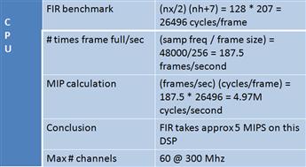
Figure 3-16: Computing the number of channels possible for a DSP system.
This FIR routine takes about 106K cycles per frame. Now, consider the sampling frequency. A key question to answer at this point is, ‘How many times is a frame FULL per second?’ To answer this, divide the sampling frequency (which specifies how often a new data item is sampled) by the size of the buffer. Performing this calculation determines that we fill about 47 frames per second.
Next is the most important calculation – how many MIPS does this algorithm require of a processor? We need to find out how many cycles this algorithm will require per second. Now we multiply frames/second by cycles/frame and perform the calculation using this data to get a throughput rate of about 5 MIPS. Assuming this is the only computation being performed on the processor, the channel density (how many channels of simultaneous processing can be performed by a processor) is a maximum of 300/5 = 60 channels. This completes the CPU calculation. This result cannot be used in the I/O calculation.
Algorithm: 200-tap (nh) low-pass FIR filter
Frame size: 256 (nx) 16-bit elements
Sampling frequency: 48 kHz
The next question to answer is ‘Can the I/O interface feed the CPU fast enough to handle 60 channels?’ Figure 3-17 shows this. Step one is to first calculate the ‘bit rate’ required of the serial port. To do this, the required sampling rate (48 kHz) is multiplied by the maximum channel density (60). This is then multiplied by 16 (assuming the word size is 16 – which it is, given the chosen algorithm). This calculation yields a requirement of 46 Mbps for 60 channels operating at 48 kHz. In this example what can the DSP serial port support? The specification says that the maximum bit rate is 50 Mbps (1/2 the CPU clock rate up to 50 Mbps). This tells us that the processor can handle the rates we need for this chosen application. Can the DMA move these samples from the McBSP to memory fast enough? Again, the specification tells us that this should not be a problem.
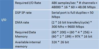
Figure 3-17: Computing maximum number of channels and required memory and I/O.
The next step considers the issue of required data memory.
Assume that all 60 channels of this application are using different filters – i.e., 60 different sets of coefficients and 60 double buffers (this can be implemented using a ping pong buffer on both the receive and transmit sides. This is a total of 4 buffers per channel, hence the ∗4 + the delay buffers for each channel (only the receive side has delay buffers, so the algorithm becomes:
Number of channels ∗ 2 ∗ delay buffer size
= 60 ∗ 2 ∗ 199
This is extremely conservative and the system designer could save some memory if this is not the case. But this is a worst case scenario. So, we’ll have 60 sets of 200 coefficients, 60 double buffers (ping and pong on receive and transmit, hence the ∗4) and we’ll also need a delay buffer of the number of coefficients –1, which is 199 for each channel. So, the calculation is:
(#Channels ∗ #coefficients) + (#Channels ∗ 4 ∗ frame size) + (#Channels ∗ #delay_buffers ∗ delay_buffer_size)
= (60 ∗ 200) + (60 ∗ 4 ∗ 256) + (60 ∗ 2 ∗ 199)
This results in a requirement of 97K of memory. The DSP only has 32K of on-chip memory, so this is a limitation. Again, you can re-do the calculation assuming only one type of filter is used, or look for another processor.
Once you’ve done these calculations, you can ‘back off’ the calculation to the exact number of channels your system requires, determine an initial theoretical CPU load that is expected, and then make some decisions about what to do with any additional bandwidth that is left over.
There are two sample cases that help drive discussion on issues related to CPU load. In the first case, the entire application only takes 20% of the CPU’s load. What do you do with the extra bandwidth? The designer can add more algorithmic processing, increase the channel density, increase the sampling rate to achieve higher resolution or accuracy, or decrease the clock/voltage so that the CPU load goes up and you save lots of power. It is up to the system designer to determine the best strategy here based on the system requirements.
The second example application is the other side of the fence – where the application takes more processing power than the CPU can handle. This leads the designer to consider a combined solution. The architecture of this again depends on the application’s needs.
DSP software
DSP software development is primarily focused on achieving the performance goals of the system. It is more efficient to develop DSP software using a higher level language like C or C++ but it is not uncommon to see some of the high performance, MIPS-intensive algorithms written, at least partially, in assembly language. When generating DSP algorithm code, the designer should use one or more of the following approaches:
• Find existing algorithms (free code).
• Buy or license algorithms from vendors. These algorithms may come bundled with tools or may be classes of libraries for specific applications.
• Write the algorithms in house. If using this approach, implement as much of the algorithm as possible in C/C++. This usually results in faster time to market and requires a common skill found in the industry.
It is much easier to find a C programmer than a DSP assembly language programmer. DSP compiler efficiency is fairly good and significant performance can be achieved using a compiler with the right techniques. There are several tuning techniques used to generate optimal code and this will be discussed in later chapters.
To tune your code and get the highest efficiency possible, the system designer needs to know three things:
There are several ways to help the compiler generate efficient code. Compilers are pessimistic by nature, so the more information that can be provided about the system algorithms, where data is in memory, etc., the better. The DSP compiler can achieve 100% efficiency versus hand-coded assembly if the right techniques are used. There are pros and cons to writing DSP algorithms in assembly language as well, so if this must be done, these must be understood from the beginning.
The compiler is generally part of a more comprehensive integrated development environment (IDE) that includes a number of other tools. Figure 3-18 shows some of the main components of a DSP IDE including real-time analysis, simulation, user interfaces, and code generation capabilities.
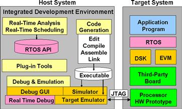
Figure 3-18: Main components of a DSP IDE.
DSP IDEs also provide several components for use on the target application side including a real-time operating system, network stacks, low level drivers (LLDs), APIs, abstraction layers, and other support software as shown in Figure 3-19. This allows DSP developers to get systems up and running quickly.
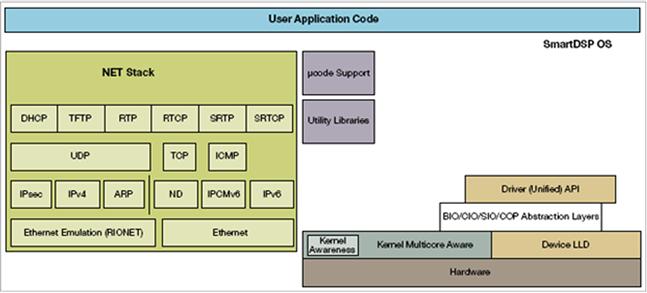
Figure 3-19: DSP RTOS component architecture.
Code tuning and optimization
One of the main differentiators between developers of non-real-time systems and real-time systems is the phase of code tuning and optimization. It is during this phase that the DSP developer looks for ‘hot spots’ or inefficient code segments and attempts to optimize those segments. Code in real-time DSP systems is often optimized for speed, memory size, or power. DSP code build tools (compilers, assemblers, and linkers) are improving to the point where developers can write the majority, if not all, of their application in high-level languages like C or C++. Nevertheless, the developer must provide help and guidance to the compiler in order to get the technology entitlement from the DSP architecture.
DSP compilers perform architecture-specific optimizations and provide the developer with feedback on the decisions and assumptions that were made during the compile process. The developer must iterate in this phase, to address the decisions and assumptions made during the build process, until the performance goals are met. DSP developers can give the DSP compiler specific instructions using a number of compiler options. These options direct the compiler as to the level of aggressiveness to use when compiling the code, whether to focus on code speed or size, whether to compile with advanced debug information, and many other options.
Given the potentially large number of degrees of freedom in compile options and optimization axes (speed, size, power), the number of trade-offs available during the optimization phase can be enormous (especially considering that every function or file in an application can be compiled with different options (see Figure 3-20)). Profile-based optimization can be used to graph a summary of code size versus speed options. The developer can choose the option that meets the goals for speed and power and have the application automatically built with the option that yields the selected size/speed trade-off selected.
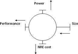
Figure 3-20: Optimization trade-offs between size, power, performance, and cost.
Typical DSP development flow
DSP developers follow a development flow that takes them through several phases:
• Application Definition – it’s during this phase that the developer begins to focus on the end goals for performance, power, and cost.
• Architecture Design – during this phase, the application is designed at a systems level using block diagram and signal flow tools if the application is large enough to justify using these tools.
• Hardware/ Software mapping – in this phase a target decision is made for each block and signal in the architecture design
• Code Creation – this phase is where the initial development is done, prototypes are developed, and mockups of the system are performed.
• Validate /Debug – functional correctness is verified during this phase
• Tuning /Optimization – this is the phase where the developer’s goal is to meet the performance goals of the system
Developing a well-tuned and optimized application involves several iterations between the validate phase and the optimize phase. Each time through the validate phase the developer will edit and build the modified application, run it on a target or simulator, and analyze the results for functional correctness. Once the application is functionally correct, the developer will begin a phase of optimization on the functionally correct code. This involves tuning the application toward the performance goals of the system (speed, memory, power, for example), running the tuned code on the target or simulator to measure the performance, and evaluation where the developer will analyze the remaining ‘hot spots’ or areas of concern that have not yet been addressed, or are still outside the goals of performance for that particular area (see Figure 3-21).
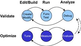
Figure 3-21: DSP developers iterate through a series of optimize-and-validate steps until the goals for performance are achieved.
Once the evaluation is complete, the developer will go back to the validate phase where the new, more optimized code is run to verify functional correctness has not been compromised. If the performance of the application is within acceptable goals for the developer, the process stops. If a particular optimization has broken the functional correctness of the code, the developer will debug the system to determine what has broken, fix the problem, and continue with another round of optimization. Optimizing DSP applications inherently leads to more complex code, and the likelihood of breaking something that used to work increases the more aggressively the developer optimizes the application. There can be many cycles in this process, continuing until the performance goals have been met for the system.
Generally, a DSP application will initially be developed without much optimization. During this early period, the DSP developer is primarily concerned with functional correctness of the application. Therefore, the ‘out of box’ experience from a performance perspective is not that impressive, even when using the more aggressive levels of optimization in the DSP compiler. This initial view can be termed the ‘pessimistic’ view, in the sense that there are no aggressive assumptions made in the compiled output, there is no aggressive mapping of the application to the specific DSP architecture, and there is no aggressive algorithmic transformation to allow the application to run more efficiently on the target DSP.
Significant performance improvements can come quickly by focusing on a few critical areas of the application:
• Key tight loops in the code with many iterations
The techniques to perform these optimizations are discussed in the chapter on optimizing DSP software. If these few key optimizations are performed, the overall system performance goes up significantly. As Figure 3-22 shows, a few key optimizations on a small percentage of the code really leads to significant performance improvements. Additional phases of optimization get more and more difficult as the optimization opportunities are reduced, as well as the cost/benefit of each additional optimization. The goal of the DSP developer must be to continue to optimize the application until the performance goals of the system are met, not until the application is running at its theoretical peak performance. The cost/benefit does not justify this approach.
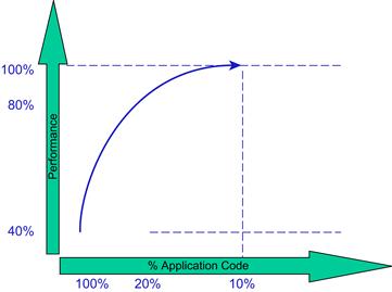
Figure 3-22: Optimizing DSP code takes time and effort to reach the desired performance goals.
After each optimization, the profiled application can be analyzed for where the majority of cycles or memory is being consumed by the application. DSP IDEs provide advanced profiling capabilities that allow the DSP developer to profile the application and display useful information about the application such as code size, total cycle count, and number of times the algorithm looped through a particular function. This information can then be analyzed to determine which functions are optimization candidates (Figure 3-23).
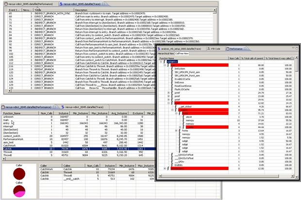
Figure 3-23: Profiling and determining hot spots in DSP applications is a common exercise, and tools can aid in this process.
An optimal approach to profiling and tuning a DSP application is to attack the right areas first. These represent those areas where the greatest performance improvement can be gained with the smallest effort. A Pareto ranking of the biggest performance areas will guide the DSP developer towards those areas where the most performance can be gained.
Generally, the top eight to ten performance intensive algorithms in the DSP system are measured, analyzed, and then optimized to achieve full system performance goals. Figure 3-24 is an example of an actual set of benchmarks used to assess full system performance goals. Although there were over 200 algorithms in the system, none were chosen due to the fact that they consumed a majority of the cycles. This then became the suite of benchmarks on which to focus the optimization process.
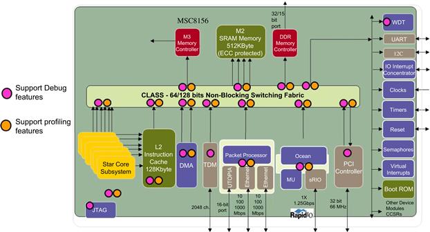
Figure 3-24: Advanced DSP SoCs have peripherals, communication busses, cores, and accelerators instrumented with counters and timers to support both profiling and debug.
In order to get a good system view of where the cycles are being consumed, on-chip instrumentation in the form of counters, timers, etc., are used to enable the extraction of various types of profiling and debug data. Advanced DSP SoCs have peripherals, communication busses, cores, and accelerators instrumented with counters and timers to support both profiling and debug. This is shown in Figure 3-25 for a six core multicore DSP device. By having this support on chip, software tools, profilers, and even the running application software can take advantage of this information, to make decisions about optimization, debug, etc. This allows the DSP developer to visualize debug and profiling information at various points in the DSP system including the cores, the communication fabric, the accelerators and peripherals, and other important processing elements in the SoC, which allows for full system analysis (Figure 3-27).
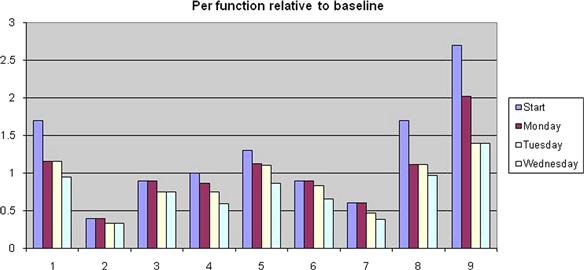
Figure 3-25: Generally the top eight to ten performance intensive algorithms in the DSP system are measured, analyzed, and then optimized to achieve full system performance goals.
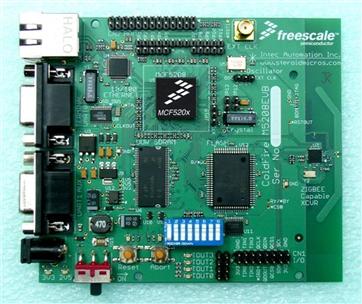
Figure 3-26: Evaluation board for DSP.
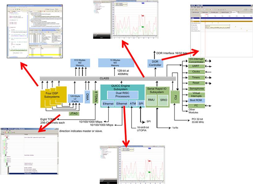
Figure 3-27: Visibility must be provided throughout the DSP SoC.
A DSP starter kit (Figure 3-26) is easy to install and allows the developer to get started writing code very quickly. The starter kits usually come with daughter card expansion slots, the target hardware, software development tools, a parallel port interface for debug, a power supply, and the appropriate cables.
Putting it all together
There are five major stages to the DSP development process:
• System concept and requirements – this phase includes the elicitation of the system level functional and non-functional (sometimes called ‘quality’) requirements. Power requirements, quality of service (QoS), performance and other system level requirements are elicited. Modeling techniques such as signal flow graphs are constructed to examine the major building blocks of the system.
• System algorithm research and experimentation – during this phase, the detailed algorithms are developed based on the given performance and accuracy requirements. Analysis is first done on floating point development systems to determine if these performance and accuracy requirements can be met. These systems are then ported, if necessary, to fixed point processors for cost reasons. Inexpensive evaluation boards are used for this analysis.
• System design – during the design phase, the hardware and software blocks for the system are selected and/or developed. These systems are analyzed using prototyping and simulation to determine whether the right partitioning has been performed and whether the performance goals can be realized using the given hardware and software components. Software components can be custom developed or reused, depending on the application.
• System implementation – during the system implementation phase, inputs from system prototyping, trade-off studies, and hardware synthesis options are used to develop a full system co-simulation model. Software algorithms and components are used to develop the software system. Combinations of signal processing algorithms and control frameworks are used to develop the system.
• System integration – during the system integration phase, the system is built, validated, tuned, if necessary, and executed in a simulated environment or in hardware in the loop simulation environment. The scheduled system is analyzed and potentially re-partitioned if performance goals are not being met.
In many ways, the DSP system development process is similar to other development processes. Given the increased amount of signal processing algorithms, early simulation-based analysis is required more for these systems. The increased focus on performance requires the DSP development process to focus more on real-time deadlines and iterations of performance tuning.