
Chapter 5. CUDA Memory
High-performance GPGPU applications require reuse of data inside the SM. The reason is that on-board global memory is simply not fast enough to meet the needs of all the streaming multiprocessors on the GPU. Data transfers from the host and other GPGPUs further exacerbate the problem as all DMA (Direct Memory Access) operations go through global memory, which consumes additional memory bandwidth. CUDA exposes the memory spaces within the SM and provides configurable caches to give the developer the greatest opportunity for data reuse. Managing the significant performance difference between on-board and on-chip memory to attain high-performance needs is of paramount importance to a CUDA programmer.
Keywords
Memory, global memory, register memory, shared memory, texture memory, constant memory, L2 cache
High-performance GPGPU applications require reuse of data inside the SM. The reason is that on-board global memory is simply not fast enough to meet the needs of all the streaming multiprocessors on the GPU. Data transfers from the host and other GPGPUs further exacerbate the problem as all DMA (Direct Memory Access) operations go through global memory, which consumes additional memory bandwidth. CUDA exposes the memory spaces within the SM and provides configurable caches to give the developer the greatest opportunity for data reuse. Managing the significant performance difference between on-board and on-chip memory to attain high-performance needs is of paramount important to a CUDA programmer.
At the end of this chapter, the reader will have a basic understanding of:
■ Why memory bandwidth is a key gating factor for application performance.
■ The different CUDA memory types and how CUDA exposes the memory on the SM.
■ The L1 cache and importance for register spilling, global memory accesses, recursion, and divide-and-conquer algorithms.
■ Important memory-related profiler measurements.
■ Limitations on hardware memory design.
The CUDA Memory Hierarchy
The CUDA programming model assumes that the all threads execute on a physically separate device from the host running the application. Implicit is the assumption that the host and all the devices maintain their own separate memory spaces, referred to as host and device memory, 1 and that some form of bulk transfer is the mechanism of data transport.
1Some low-end devices actually share the same memory as the host, but they do not change the programming model.
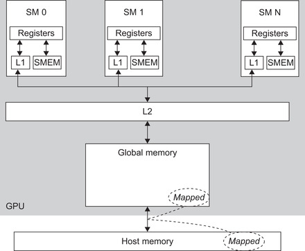
The line between the host and device memory becomes somewhat blurred when host memory is mapped into the address space of the GPU. In this way, modifications by either the device or host will be reflected in the memory space of all the devices mapping a region of memory. Pages are transparently transferred asynchronously between the host and GPU(s). Experienced programmers will recognize that mapped memory is analogous to the mmap() system call.
Uniform Virtual Addressing (UVA) is a CUDA 4.0 feature that simplifies multi-GPU programming by giving the runtime the ability to determine upon which device a region of memory resides purely on the basis of the pointer address. Semantically, UVA gives CUDA developers the ability to perform direct GPU-to-GPU data transfers with cudaMemcpy(). To use it, just register the memory region with cudaHostRegister(). Bulk data transfers can then occur between devices by calling cudaMemcpy(). The runtime will ensure that the appropriate source and destination devices are used in the transfer. The method cudaHostUnregister(ptr) terminates the use of UVA data transfers for that region of memory. See Figure 5.1.
GPU Memory
CUDA-enabled GPGPUs have both on-chip and on-board memory. The fastest and most scalable is the highly desirable on-chip SM memory. These are limited memory stores measured in kilobytes (KB) of storage. The on-board global memory is a shared memory system accessible by all the SM across the GPU. It is measured in gigabytes (GB) of memory, which is by far the largest, most commonly used, and slowest memory store on the GPU.
Benchmarks have shown the significant bandwidth differences between on-chip and off-chip memory systems (see Table 5.1). Only registers internal to the SM have the bandwidth needed to keep the SM fully loaded (without stalls) to achieve peak performance. Although the bandwidth of shared memory can greatly accelerate applications, it is still too slow to achieve peak performance (Volkov, 2010).
| Register memory | ≈8,000 GB/s |
| Shared memory | ≈1,600 GB/s |
| Global memory | 177 GB/s |
| Mapped memory | ≈8 GB/s one-way |
Managing the significant performance difference between on-board and on-chip memory is the primary concern of a CUDA programmer. To put the performance implications in perspective, consider how memory bandwidth limits the performance of the following simple calculation when it resides in global memory, in Example 5.1, “A Simple Memory-Bandwidith-Limited Calculation”:
for(i=0; i < N; i++) c[i] = a[i] * b[i];
Each floating-point multiply requires two memory reads and a write. Assuming that single-precision (32-bit or 4-byte) floating-point values are being used, a teraflop (trillion floating-point operations per second) GPU would require 12 terabytes per second (TB/s) of memory bandwidth for this calculation to run at full speed. Said another way, a GPU with 177 GB/s of memory bandwidth could only deliver 14 Gflop, or approximately 1.4 percent of the performance of a teraflop GPU. When the extra precision of 64-bit (8-byte) floating-point arithmetic is required, the reader can halve the effective computational rate. 2
2Data reuse is important on conventional processors as well. The impact tends to be less dramatic when an application becomes memory-bound because conventional systems have fewer processing cores.
Clearly, it is necessary to reuse the data within the SM to achieve high performance. Only by exploiting data locality can a programmer minimize global memory transactions and keep data in fast memory. GPGPUs support two types of locality as they accelerate both computational and rendering applications:
■ Temporal locality: assumes that a recently accessed data item is likely to be used again in the near future. Many computational applications demonstrate this LRU (Least Recently Used) behavior.
■ Spatial locality: neighboring data is cached with the expectation that spatially adjacent memory locations will be used in the near future. Rendering operations tend to have high 2D spatial locality.
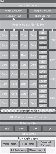
As can be seen in Figure 5.2, the SM also contains constant (labeled Uniform cache in the figure) and texture memory caches. Though desirable, the L1 and L2 caches in compute 2.0 devices have subsumed much of the capability of these memory spaces. When programming compute 1.x devices, constant memory must be used when data needs to be efficiently broadcast to all the threads. Texture memory can be used as a form of cache to avoid global memory bandwidth limitations and handle some small irregular memory accesses (Haixiang, Schmidt, Weiguo, & Müller-Wittig, 2010). However, the texture cache is relatively small—on the order of 8 KB. Of course, visualization is the intended usage and greatest value for texture memory across all compute device generations.
Compute 2.0 devices added an L1 cache to each SM and a unified L2 cache that fits between all the SM and global memory, as shown in Figure 5.1.
L2 Cache
The unified L2 (Level 2) cache is a tremendous labor-saving device that works as a fast data store accessible by all the SM on the GPU. A great many applications will suddenly run faster on compute 2.0 devices because of the L2 cache. Two reasons are:
■ Without requiring any intervention by the CUDA programmer, the L2 will cache data in an LRU fashion that allows many CUDA kernels avoid global memory bandwidth bottlenecks.
■ The L2 cache greatly speeds irregular memory access patterns that otherwise would exhibit extremely poor GPU performance. For many algorithms, this characteristic will determine whether an application can be used on compute 1.x hardware.
Fermi GPUs provide a 768 KB unified L2 cache that is guaranteed to present a coherent view to all SMs. In other words, any thread can modify a value held in the L2 cache. At a later time, any other thread on the GPU can read that particular memory address and receive the correct, updated value. Of course, atomic operations must be used to guarantee that the store (or write) transaction completes before other threads are allowed read access.
Previous GPGPU architectures had challenges with this very common read/update operation because two separate data paths were utilized—specifically, the read-only texture load path and the write-only pixel data output path. To ensure data correctness, older GPU architectures required that all participating caches along the read path be potentially invalidated and flushed after any thread modified the value of an in-cache memory location. The Fermi architecture eliminated this bottleneck with the unified L2 cache along with the need for the texture and Raster Output (ROP) caches in earlier-generation GPUs.
All data loads and stores go through the L2 cache including CPU/GPU memory copies, emphasized to stress that host data transfers might unexpectedly affect cache hits and thus application performance. Similarly, asynchronous kernel execution can also pollute the cache.
Relevant computeprof Values for the L2 Cache
L1 Cache
Compute 2.0 devices have 64 KB of L1 memory that can be partitioned to favor shared memory or dynamic read/write operations. Note that the L1 cache:
■ Is designed for spatial and not temporal reuse. Most developers expect processor caches that behave as an LRU cache. On a GPU, this mistaken assumption can lead to unexpected cache misses, as frequently accessing a cached L1 memory location does not guarantee that the memory location will stay in the cache.
■ Will not be affected by stores to global memory, as store operations bypass the L1 cache.
■ Is not coherent. The volatile keyword must be used when declaring shared memory that can be modified by threads in other blocks to guarantee that the compiler will not load the shared memory location into a register. Private data (registers, stack, etc.) can be used without concern.
■ Has a latency of 10–20 cycles.
The L1 caches per-thread local data structures such the per-thread stack. The addition of a stack allows compute 2.0 devices to support recursive routines (routines that call themselves). Many problems can be naturally expressed in a recursive form. For example, divide-and-conquer methods repeatedly break a larger problem into smaller subproblems. At some point, the problem becomes simple enough to solve directly. The solutions to the subproblems are combined to give a solution to the initial problem. The stack can consume up to 1 KB of the L1 cache.
CUDA also uses an abstract memory type called local memory. Local memory is not a separate memory system per se but rather a memory location used to hold spilled registers. Register spilling occurs when a thread block requires more register storage than is available on an SM. Pre-Fermi GPUs spilled registers to global memory, which caused a dramatic drop in application performance, as three-orders-of-magnitude-slower GB/s global memory accesses replaced TB/s register memory. Compute 2.0 and later devices spill registers to the L1 cache, which minimizes the performance impact of register spills.
If desired, the Fermi L1 cache can be deactivated with the -Xptxas -dlcm=cg command-line argument to nvcc. Even when deactivated, both the stack and local memory still reside in the L1 cache memory.
The beauty in this configurability is that applications that reuse data or have misaligned, unpredictable, or irregular memory access patterns can configure the L1 cache as a 48 KB dynamic cache (leaving 16 KB for shared memory) while applications that need to share more data amongst threads inside a thread block can assign 48 KB as shared memory (leaving 16 KB for the cache). In this way, the NVIDIA designers empowered the application developer to configure the memory within the SM to achieve the best performance.
The L1 cache is utilized when the compiler generates an LDU (LoaD Uniform) instruction to cache data that needs to be efficiently broadcast to all the threads within the SM. Previous generations of GPUs could broadcast information efficiently among all the threads in an application only from constant memory.
Compute 2.0 devices can broadcast data from global memory without requiring explicit programmer intervention, subject to the following conditions:
1. The pointer is prefixed with the const keyword.
2. The memory access is uniform across all the threads in the block as in Example 5.2, “A Uniform Memory Access Example”:
__global__ void kernel( float *g_dst, const float *g_src )
{
g_dst = g_src[0] + g_src[blockIdx.x];
}
Relevant computeprof Values for the L1 Cache
CUDA Memory Types
Table 5.4 summarizes the characteristics of the various CUDA memory spaces for compute 2.0 and later devices.
Registers
Registers are the fastest memory on the GPU. They are a very precious resource because they are the only memory on the GPU with enough bandwidth and a low enough latency to deliver peak performance.
Each GF100 SM supports 32 K 32-bit registers. The maximum number of registers that can be used by a CUDA kernel is 63, due to the limited number of bits available for indexing into the register store. The number of available registers varies on a Fermi SM:
■ If the SM is running 1,536 threads, then only 21 registers can be used.
■ The number of available registers degrades gracefully from 63 to 21 as the workload (and hence resource requirements) increases by number of threads.
Register spilling on GF100 SM increases the importance of the L1 cache because it can preserve high performance. Be aware that pressure from register spilling and the stack (which can consume 1 KB of L1 storage) can increase the cache miss rate by forcing data to be evicted.
Local memory
Local memory accesses occur for only some automatic variables. An automatic variable is declared in the device code without any of the __device__, __shared__, or __constant__ qualifiers. Generally, an automatic variable resides in a register except for the following:
■ Arrays that the compiler cannot determine are indexed with constant quantities.
■ Large structures or arrays that would consume too much register space.
■ Any variable the compiler decides to spill to local memory when a kernel uses more registers than are available on the SM.
The nvcc compiler reports total local memory usage per kernel (lmem) when compiling with the --ptxas-options=-v option. These reported values may be affected by some mathematical functions that access local memory.
Relevant computeprof Values for Local Memory Cache
Shared Memory
Shared memory (also referred to as smem) can be either 16 KB or 48 KB per SM arranged in 32 banks that are 32 bits wide. Contrary to early NVIDIA documentation, shared memory is not as fast as register memory.
Shared memory can be allocated three different ways:
1. Statically within the kernel or globally within the file as shown in the declaration in Example 5.3, “A Static Shared Memory Declaration”:
__shared__ int s_data[256];
2. Dynamically within the kernel by calling the driver API function cuFuncSetSharedSize.
3. Dynamically via the execution configuration.
Only a single block of shared memory can be allocated via the execution configuration. Using more than one dynamically allocated shared memory variable in a kernel requires manually generating the offsets for each variable. Example 5.4, “Multiple Variables in a Dynamically Allocated Shared Memory Block,” shows how to allocate and utilize two dynamically allocated shared memory vectors a and b:
__global__ void kernel(int aSize)
{
extern __shared__ float sData[];
float *a, *b;
a = sData; // a starts at the beginning of the dynamically allocated smem block
b = &a[aSize]; // b starts immediately following the end of a in the smem block
}
The kernel call would look like Example 5.5, “Execution Configuration that Dynamically Allocates Shared Memory”:
Kernel<<<nBlocks, nThreadPerBlock, nBytesSharedMemory>>>(aSize);
Shared memory is arranged in 32 four-byte-wide banks on the SM. Under ideal circumstances, 32 threads will be able to access shared memory in parallel without performance degradation. Unfortunately, bank conflicts occur when multiple requests are made by different threads for data within the same bank. These requests can either be for the same address or for multiple addresses that map to the same bank. When this happens, the hardware serializes the memory operations. If n threads within a warp cause a bank conflict, then n accesses are executed serially, causing an n-times slowdown on that SM.
The size of the memory request can also cause a bank conflict. Shared memory in compute 2.0 devices has been improved to support double-precision variables in shared memory without causing warp serialization. Previous-generation GPUs required a workaround that involved splitting 64-bit data into two 32-bit values and storing them separately in shared memory. Be aware that the majority of 128-bit memory accesses (e.g., float4) will still cause a two-way bank conflict in shared memory on compute 2.0 devices.
Padding shared memory to avoid bank conflicts represents a portability challenge. Example 5.6, “Shared Memory Padded for a GT200/Tesla C1060” illustratres an older code that
__shared__ tile [16][17];
__shared__ tile [32][33];
Notice that a column was added in the previous example to prevent a bank conflict. In this case, wasting space is preferable to accepting the performance slowdown. Without the padding, every consecutive column index access within a warp would serialize.
Shared memory has the ability to multicast, which means that if n threads within a warp access the same word at the same time, then only a single shared memory fetch occurs. Compute 2.0 devices broadcast the entire word, which means that multiple threads can access different bytes within the broadcast word without affecting performance. Whole-word broadcast was available only in 1.x devices. Subword accesses within the broadcast word, or the same bank, caused serialization.
Threads can communicate via shared memory without using the _syncthreads barrier, as long as they all belong to the same warp. See Example 5.8, “A Barrier Is Not Required When Sharing Data within a Warp”:
if (tid < 32) { … }
If shared memory is used to communicate between warps in a thread block, make certain to have volatile in front of the shared memory declaration. The volatile keyword eliminates the possibility that the compiler might silently cache the previously loaded shared memory value in a register and fail to reload it again on next reference. Due to architectural changes:
■ Compute 1.x devices access shared memory only directly as an operand.
■ Compute 2.0 devices have a load/store architecture that can bring data into registers.
Legacy codes need to add a volatile keyword to avoid errors when running on compute 2.0 devices. As shown in the following example, a simple __shared__ declaration was sufficient on compute 1.x devices. The legacy code needs to be changed, as shown in Example 5.9, “A Volatile Must Be Added to Codes that Communicate across Thread Blocks with Shared Memory”:
__shared__ int cross[32]; // acceptable for 1.x devices
// Compute 2.0 devices require a volatile
volatile __shared__ int cross[32];
Volkov notes that the trend in parallel architecture design is towards an inverse memory hierarchy where the number of registers is increasing compared to cache and shared memory. Scalability and performance are the reasons as registers can be replicated along with the SM (or the processor core in a multicore processor). More registers means that more data can be kept in high-speed memory, which means that more instructions can run without external dependencies resulting in higher performance (Volkov, 2010). He also notes that the performance gap between shared memory and arithmetic throughput has increased with Fermi, raising concerns that the current shared memory hardware on the Fermi architecture is a step backward (Volkov, 2010).
Table 5.6 shows the ratio of shared memory banks to thread processors compared to the number of registers per thread.
For portability, performance, and scalability reasons, it is highly recommended that registers be used instead of shared memory whenever possible.
Relevant computeprof Values for Shared Memory
Constant Memory
For compute 1.x devices, constant memory is an excellent way to store and broadcast read-only data to all the threads on the GPU. The constant cache is limited to 64 KB. It can broadcast 32-bits per warp per two clocks per multiprocessor and should be used when all the threads in a warp read the same address. Otherwise, the accesses will serialize on compute 1.x devices.
Compute 2.0 and higher devices allow developers to access global memory with the efficiency of constant memory when the compiler can recognize and use the LDU instruction. Specifically, the data must:
■ Reside in global memory.
■ Be read-only in the kernel (programmer can enforce this using the const keyword).
■ Must not depend on the thread ID.
See Example 5.10, “Examples of Uniform and Nonuniform Constant Memory Accesses”:
__global__ void kernel( const float *g_a )
{
float x = g_a[15]; // uniform
float y = g_a[blockIdx.x + 5] ; // uniform
float z = g_a[threadIdx.x] ; // not uniform !
}
There is no need for __constant__ declaration; plus, there is no fixed limit to the amount of data, as is the case with constant memory. Still, constant memory is useful on compute 2.0 devices when there is enough pressure on the cache to cause eviction of the data that is to be broadcast.
Constant memory is statically allocated within a file. Only the host can write to constant memory, which can be accessed via the runtime library methods: cudaGetSymbolAddress(), cudaGetSymbolSize(), cudaMemcpyToSymbol(), and cudaMemcpyFromSymbol(), plus cuModuleGetGlobal() from the driver API.
Texture Memory
Textures are bound to global memory and can provide both cache and some limited, 9-bit processing capabilities. How the global memory that the texture binds to is allocated dictates some of the capabilities the texture can provide. For this reason, it is important to distinguish between three memory types that can be bound to a texture (see Table 5.8).
For CUDA programmers, the most salient points about using texture memory are:
■ Texture memory is generally used in visualization.
■ The cache is optimized for 2D spatial locality.
■ It contains only 8 KB of cache per SM.
■ Textures have limited processing capabilities that can efficiently unpack and broadcast data. Thus, a single float4 texture read is faster than four separate 32-bit reads.
■ Textures have separate 9-bit computational units that perform out-of-bounds index handling, interpolation, and format conversion from integer types (char, short, int) to float.
■ A thread can safely read some texture or surface memory location only if this memory location has been updated by a previous kernel call or memory copy, but not if it has been previously updated by the same thread or another thread from the same kernel call.
It is important to distinguish between textures bound to memory allocated with cudaMalloc() and those bound to padded memory allocated with cudaMallocPitch().
■ When using the texture only as a cache: In this case, programmers might consider binding the texture memory created with cudaMalloc(), because the texture unit cache is small and caching the padding added by cudaMallocPitch() would be wasteful.
■ When using the texture to perform some processing: In this case, it is important to bind the texture to padded memory created with cudaMallocPitch() so that the texture unit boundary processing works correctly. In other words, don't bind linear memory created with cudaMalloc() and attempt to manually set the pitch to a texture because unexpected things might happen—especially across device generations.
Depending on how the global memory bound to the texture was created, there are several possible ways to fetch from the texture that might also invoke some form of texture processing by the texture.
The simplest way to fetch data from a texture is by using tex1Dfetch() because:
■ Only integer addressing is supported.
■ No additional filtering or addressing modes are provided.
Use of the methods tex1D(), tex2D(), and tex3D() are more complicated because the interpretation of the texture coordinates, what processing occurs during the texture fetch, and the return value delivered by the texture fetch are all controlled by setting the texture reference's mutable (runtime) and immutable (compile-time) attributes:
■ Immutable parameters (compile-time).
■ Type: type returned when fetching
- Basic integer and float types
- CUDA 1-, 2-, 4-element vectors
■ Dimensionality:
- Currently 1D, 2D, or 3D
■ Read mode:
- cudaReadModeElementType
- cudaReadModeNormalizedFloat (valid for 8- or 16-bit integers). It returns [–1,1] for signed, [0,1] for unsigned
■ Mutable parameters (runtime, only for array textures and pitch linear memory).
■ Normalized:
- Nonzero = addressing range [0,1]
■ Filter mode:
- cudaFilterModePoint
- cudaFilterModeLinear
■ Address mode:
- cudaAddressModeClamp
- cudaAddressModeWrap
By default, textures are referenced using floating-point coordinates in the range [0,N) where N is the size of the texture in the dimension corresponding to the coordinate. Specifying that normalized texture coordinates will be used implies all references will be in the range [0,1).
The wrap mode specifies what happens for out-of-bounds addressing:
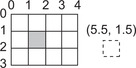
■ Wrap: out-of-bounds coordinates are wrapped (via modulo arithmetic), as shown in Figure 5.3.
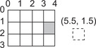
■ Clamp: out-of-bounds coordinates are replaced with the closest boundary, as shown in Figure 5.4.
Linear texture filtering may be performed only for textures that are configured to return floating-point data. A texel, short for “texture element,” is an element of a texture array. Thus, linear texture filtering performs low-precision (9-bit fixed-point with 8-bits of fractional value) interpolation between neighboring texels. When enabled, the texels surrounding a texture fetch location are read and the return value of the texture fetch is interpolated by the texture hardware based on where the texture coordinates fell between the texels. Simple linear interpolation is performed for one-dimensional textures, as shown in Equation 5.1, “Texture linear interpolation.”
(5.1)
Similarly, the dedicated texture hardware will perform bilinear and trilinear filtering for higher-dimensional data.
As long as the 9-bits of accuracy can be tolerated, the dedicated texture units offer an innovative opportunity to gain even greater performance from GPU computing. One example is “GRASSY: Leveraging GPU Texture Units for Asteroseismic Data Analysis” (Townsend, Sankaralingam, & Sinclair, 2011).
Relevant computeprof Values for Texture Memory
Complete working examples utilizing texture memory can be found in Part 13 of my Doctor Dobb's Journal tutorial series (http://drdobbs.com/cpp/218100902).
Global Memory
Understanding how to efficiently use global memory is an essential requirement to becoming an adept CUDA programmer. Focusing on data reuse within the SM and caches avoids memory bandwidth limitations. This is the third most important rule of high-performance GPGPU programming, as introduced in Chapter 1:
1. Get the data on the GPGPU and keep it there.
2. Give the GPGPU enough work to do.
3. Focus on data reuse within the GPGPU to avoid memory bandwidth limitations.
At some point, it is not possible to avoid global memory, in which case it is essential to understand how to use global memory effectively. In particular, the Fermi architecture made some important changes in how CUDA programmers need to think about and use global memory.
From the developer's perspective, it cannot be stressed too strongly that all global memory accesses need to be perfectly coalesced. A coalesced memory access means that the hardware can coalesce, or combine, the memory requests from the threads into a single wide memory transaction. Best performance occurs when:
■ The memory address is aligned. The NVIDIA CUDA C Best Practices Guide points out that misaligned accesses can cause an 8 times reduction in global memory bandwidth on older devices. A Fermi GPU with caching enabled would see around a 15 percent drop (Micikevicius, 2010). The authors of the NVIDIA guide note that, “Memory allocated through the runtime API, such as via cudaMalloc(), is guaranteed to be aligned to at least 256 bytes. Therefore, choosing sensible thread block sizes, such as multiples of 16, facilitates memory accesses by half warps that are aligned to segments. In addition, the qualifiers __align__(8) and __align__(16) can be used when defining structures to ensure alignment to segments.” (CUDA C Best Practices Guide p. 27)
■ A warp accesses all the data within a contiguous region, which means that the wider memory transaction is 100 percent efficient because every byte retrieved is utilized.
As discussed in Chapter 4, try to keep enough memory requests in flight to fully utilize the global memory subsystem:
■ From an ILP perspective, attempt to process several elements per threads to pipeline multiple loads. A side benefit is that indexing calculations can often be reused.
■ From a TLP perspective, launch enough threads to maximize throughput.
Analyze the memory requests in your application via the source code and profiler output. Experiment with the caching configurations and shared memory vs. L1 cache configuration to see what works best.
From a hardware perspective memory requests are issued in groups of 32 threads (as opposed to 16 in previous architectures), which matches the instruction issue width. Thus, the 32 addresses of a warp should ideally address a contiguous, aligned region to stream data from global memory at the highest bandwidth.
There are two types of loads from global memory:
■ Caching loads: This is the default mode. A memory fetch transaction attempts to find the data in the L1 and then the L2 caches. Failing that, a 128-byte cache line load is issued.
■ Noncaching loads: When lots of data needs to be fetched but not from consecutive addresses, better performance might be achieved by turning off the L1 cache with the nvcc command-line option -Xptxas -dlcm=gc. In this case, the SM does not look to see whether the data is in the L1, but it will invalidate the cache line if it is already in the L1. If the data is not in the L2, then a 32-byte global memory load is issued. This can deliver better data utilization when a 128-byte cache line fetch would be wasteful.
Global memory store transactions occur by invalidating the L1 cache line and then writing to the L2. Only when it's evicted is the L2 data actually written to global memory.
Most applications will benefit from the cache because it performs coalesced global memory loads and stores in terms of a 128-byte cache line size. Once data is inside the L2 cache, applications can reuse data, perform irregular memory accesses, and spill registers without incurring the dramatic slowdown seen in older-generation GPUs caused by having to rely on round trips to the much slower global memory. For performance reasons and transparency reasons, the L1 and L2 caches in compute 2.0 devices are a very good thing.
Common Coalescing Use Cases
Some common use cases for accessing global memory are shown with caching enabled (Table 5.10) and disabled (Table 5.11).
Global memory on the GPU was designed to quickly stream memory blocks of data into the SM. Unfortunately, loops that perform indirect indexing, utilize pointers to varying regions in memory, or that have an irregular or a large stride break this assumption. As can be seen in Table 5.10, scattered reads can reduce global memory throughput to only 3.125% of the hardware capability. Turning off the cache can provide a 4-times speed improvement, which is good but still starves the SM for data, as it provides only 12.5% of the potential global memory bandwidth.
Allocation of Global Memory
Memory can be statically allocated in device memory with a declaration:
__device__ int gmemArray[SIZE];
When using the runtime API, linear (or 1D) regions of global memory can be dynamically allocated with cudaMalloc() and freed with cudaFree(). The Thrust API internally uses cudaMalloc().
■ Memory is aligned on 256-byte boundaries.
■ For 2D accesses to be fully coalesced, both the width of the thread block and the width of the array must be a multiple of the warp size (or only half the warp size, for devices of compute capability 1.x). The runtime cudaMallocPitch() and driver API cuMemAllocPitch() methods pad the array allocation appropriately for the destination device. The associated memory copy functions described in the reference manual must be used with pitch linear memory.
Memory can be dynamically allocated in the kernel using the standard C-language malloc() and free(). It is aligned on 16-byte boundaries.
Dynamic global memory allocation on the device is supported only by devices of compute capability 2.x. Memory allocated by a given CUDA thread via malloc() remains allocated for the lifetime of the CUDA context, or until it is explicitly released by a call to free(). Any thread can use memory allocated by any other CUDA thread – even in later kernel launches. Be aware that any CUDA thread may free memory allocated by another thread, which means that care must be taken to ensure that the same pointer is not freed more than once. The CUDA memory checker, cuda-memcheck, is a useful tool to help find memory errors.
The device heap must be created before any kernel can dynamically allocate memory. By default, CUDA creates a heap of 8MB. Unlike the heap on a conventional processor, the heap on the GPU does not resize dynamically. Further, the size of the heap cannot be changed once a kernel module has loaded. Memory reserved for the device heap consumes space just like memory allocated through host-side CUDA API calls such as cudaMalloc().
The following API functions get and set the heap size:
■ Driver API:
■ cuCtxGetLimit(size_t* size, CU_LIMIT_MALLOC_HEAP_SIZE).
■ cuCtxSetLimit(CU_LIMIT_MALLOC_HEAP_SIZE, size_t size).
■ Runtime API:
■ cudaDeviceGetLimit(size_t* size, cudaLimitMallocHeapSize).
■ cudaDeviceSetLimit(cudaLimitMallocHeapSize, size_t size).
The heap size granted will be at least size bytes. cuCtxGetLimit and cudaDeviceGetLimit return the currently requested heap size.
The CUDA C Programming Guide Version 4.0 provides simple working examples of per-thread, per-threadblock, and allocation persistence across kernel invocations.
Limiting Factors in the Design of Global Memory
Global memory does represent a scaling challenge for GPGPU architects. Although multiple memory subsystems can be combined to deliver blocks of data at the aggregate performance of the combined memory systems, limiting factors such as cost, power, heat, space, and reliability prevent memory bandwidth from scaling as fast as computational throughput.
The Fermi memory subsystem provides the combined memory bandwidth of six partitions of GDDR5 memory on GF100 hardware. With this design, the GPGPU hardware architects were able to increase memory bandwidth by a factor of six over a single partition. There is no longer a linear mapping between addresses and partitions, so typical access patterns are unlikely to all fall into the same partition. This design avoids partition camping (bottlenecking on a subset or even a single controller).
The Fermi memory system supports ECC memory on high-end cards, but this feature is disabled on consumer cards. ECC is also used on memory internal to the SM. Using error correcting memory with ECC is a “must have” when deploying large numbers of GPUs in datacenter and supercomputer installations to ensure that data-sensitive applications like medical imaging, financial options pricing, and scientific simulations are protected from memory errors. ECC can be turned off at the driver level to gain an additional 20 percent in memory bandwidth and added memory capacity, which can benefit global memory bandwidth-limited applications and can be an acceptable optimization for noncritical applications. The Linux nvidia-smi command added a -e option for controlling ECC. There is a control panel option to enable or disable ECC in Windows.
There are three ways to increase the hardware bandwidth of memory in a system:
1. Increase the memory clock rate. Faster memory is more expensive, it consumes more power (which means that heat is generated), and faster memory can be more error-prone.
2. Increase the bus width. This option requires that the GPU chip have lots of pins for the memory interface. No matter how small the lithography of the manufacturing process, it is possible to fit only a limited number of physical pin connectors in a given space. More pins means that the size of the chip must be increased, which leads to a vicious cycle, as manufacturing larger chips means that fewer chips can be made per wafer, thereby driving up the cost. In a competitive market for consumer products, higher costs quickly make products unattractive so they do not sell well. Consumer products are the market that is really driving the economics of GPGPU development, which makes cost a critical factor. Optical connectors offer the potential to break this vicious cycle, but this technology has not yet matured enough to be commonly used in manufacturing.
3. Transmit more data per pin per clock. This is the magic behind GDDR5 (Graphics Double Data Rate version 5) memory and the hope behind optical connectors. Basically, the channel capacity can be calculated from the physical properties of the channel. For example, the Nyquist sampling theorem lets us determine the maximum possible data rate based on the frequency of the channel in the absence of noise. Increasing the frequency of a channel means that more data can be transmitted per unit time. Unfortunately, high-frequency electrical signals are prone to noise. The Shannon theorem tells us the maximum theoretical information transfer rate in the presence of noise, but it is up to the engineers and standards committees to make the magic of higher bandwidth data transmission happen.
Relevant computeprof Values for Global Memory
Summary
CUDA makes various hardware spaces available to the programmer. It is essential that the CUDA programmer utilize the available memory spaces to best advantage given the three orders of magnitude difference in bandwidth (from 8 TB/s register bandwidth to 8 GB/s for PCIe-limited mapped memory) between the various CUDA memory types. Failure to do so can result in poor performance.
CUDA provides a number of excellent measured and derived profile information to help track down memory bottlenecks. Understanding the characteristics of each memory type is a prerequisite to adept CUDA programming. Automated analysis by the CUDA profilers can point the developer in the right direction. Knowing how to read the profiler output is a core skill in creating high-performance applications. Otherwise, finding application bottlenecks becomes a matter of guesswork. Similarly, the CUDA memory checker can help find errors in using memory.
..................Content has been hidden....................
You can't read the all page of ebook, please click here login for view all page.