Uncertainty aspects
Abstract
This chapter deals with uncertainty aspects of measuring systems. It starts with a review of the most important terms expressing sensor behavior, as a tool for making a fair assessment of the system’s requirements and performance. The effect of intrinsic sensor limitations can be reduced by special configurations and procedures. They are also effective against errors caused by environmental influences. Methods to reduce errors due to sensor deficiencies and environmental factors are compensation, feedback, filtering, modulation and demodulation, and correction.
Keywords
Sensor specifications; additive and multiplicative errors; error compensation; measurement bridge; feedback; modulation; modulators; synchronous detection
No sensor is perfect. The mechatronic designer must be aware of the sensor’s shortcomings in order to be able to properly evaluate measurement results and to make a correct assessment of the system performance. Specifying sensor quality in terms of only accuracy is not sufficient: a larger number of precisely defined parameters are necessary to fully characterize the sensor’s behavior. Often a designer can reduce the effects of the intrinsic sensor limitations by the application of special configurations, procedures, and methods. Similar measures can also be considered when environmental influences should be eliminated. This chapter reviews the most important terms to express sensor behavior and presents some general design methods to reduce errors due to sensor deficiencies and environmental factors.
3.1 Sensor specification
Imperfections of a sensor are usually listed in the data sheets provided by the manufacturer. These sensor specifications inform the user about deviations from the ideal behavior. The user must accept technical imperfections, as long as they do not exceed the specified values.
Any measuring instrument, and hence any sensor, has to be fully specified with respect to its performance. Unfortunately, many data sheets show lack of clarity and completeness. Gradually, international agreements about formal error descriptions are being established. An exhaustive description of measurement errors and error terminology can be found in Refs [1,2], along with an international standard on transducer nomenclature and terminology [3]. Various international committees are working toward a uniform framework to specify sensors [4]. Finally, a special document, containing definitions of measurement-related terms, is in progress: the International Vocabulary of Basic and General Terms in Metrology (short VIM) [5].
The characteristics that describe sensor performance can be classified into four groups:
- • Static characteristics, describing the performance with respect to very slow changes in the measurand (the quantity that has to be measured) and in environmental conditions (e.g., temperature effecting the sensitivity or scale factor, offset and drift).
- • Dynamic characteristics, specifying the sensor response to fast variations in the measurand (e.g., bandwidth and step response).
- • Environmental characteristics, relating the sensor performance after or during exposure to specified external conditions (such as pressure, temperature, vibrations, shock, and radiation).
- • Reliability characteristics, describing the sensor’s life expectancy.
Errors that are specific for certain sensor types are discussed in the chapters concerned. In this section we first define some general specifications:
3.1.1 Sensitivity
The sensitivity of a sensor is defined as the ratio between a change in the output value and the change in the input value that causes that output change. Mathematically, the sensitivity is expressed as S=dy/dx, where x is the input signal (measurand) and y is the output signal (an electrical signal). Usually a sensor is also sensitive to changes in quantities other than the intended input quantity, such as the ambient temperature or the supply voltage. These unwelcome sensitivities should be specified as well, for a proper interpretation of the measurement result. To have a better insight in the effect of such unwanted sensitivities, they are often related to the sensitivity of the measurement quantity itself.
3.1.2 Nonlinearity and hysteresis
If the output y is a linear function of the input x, the sensitivity S does not depend on x. In the case of a nonlinear transfer function y=f(x), S does depend on the input or output value. Often, a linear response is preferred to reduce computational burden in, for instance, multisensor control systems. In that case the sensitivity can be expressed with a single parameter. Furthermore, nonlinearity introduces harmonics of the input signal frequencies, which may obstruct proper frequency analysis of the physical signals.
The transfer of a sensor with a slight nonlinearity may be approximated by a straight line, to specify its sensitivity by just one number. The user should be informed about the deviation from the actual transfer; this is specified by the nonlinearity error.
The linearity error of a system is the maximum deviation of the actual transfer characteristic from a prescribed straight line. Manufacturers specify linearity in various ways, for instance as the deviation in input or output units: Δxmax or Δymax, or as a fraction of FS (full scale): Δxmax/xmax. Nonlinearity should always be given together with a specification of the straight line. The following definitions are in use:
- • Terminal nonlinearity: Based on the terminal line: a straight line between 0% and 100% theoretical full-scale points.
- • End-point nonlinearity: Based on the end-point line, the straight line between the calibrated end points of the range; coincides with the terminal (theoretical) line after calibration of zero and scale.
- • Independent nonlinearity: Referring to the best-fit straight line, according to a specified error criterion. For instance the line midway between two parallel lines enclosing all calibration points; if the least square error criterion for the best-fit straight line is used, this linearity error is the least square nonlinearity.
- • Least square nonlinearity: Based on the least square line, the line for which the summed squares of the residuals is minimized.
Hysteresis is the maximum difference in output signal when the measurand first increases over a specified range and then returns to the starting value. The traveled range should be specified because hysteresis strongly depends on it.
3.1.3 Resolution
The resolution indicates the smallest detectable increment of the input quantity. When the measurand varies continuously, the sensor output might show discontinuous steps. The value of the corresponding smallest detectable change in the input variable is the resolution: Δxmin. Sometimes this parameter is related to the maximum value xmax that can be processed (full-scale value), resulting in the resolution expressed as Δxmin/xmax or xmax/Δxmin. This mixed use of definitions seems confusing, although it is easy to see from the units or the value itself which definition is used.
3.1.4 Accuracy
Formally, the accuracy reflects the closeness of the agreement between the actual measurement result and a true value of the measurand. The accuracy specification should include relevant conditions and other quantities. Many sensor manufacturers specify the sensor performance in terms of accuracy. This specification should be viewed with suspicion because it may or may not include particular imperfections of the sensor (e.g., nonlinearity, hysteresis, and drift) and may be only valid under strict conditions. Precision is not the same as accuracy. Actually, the term precision should not be used in any case, to avoid confusion.
3.1.5 Offset and zero drift
Most sensors are designed such that the output is zero at zero input. If the transfer characteristic does not intersect the origin (x,y=0,0), the system is said to have offset. The offset is expressed in terms of the input or the output quantity. Specifying the input offset is preferred, to facilitate a comparison with the value of the measurand.
A nonzero offset arises mainly from component tolerances. Offset compensation can be performed in the interface electronics or the signal processing unit. Once adjusted to zero, the offset may nevertheless change, due to temperature variations, changes in the supply voltage or aging effects. This relatively slow change in the offset is called zero drift. In particular, the temperature-induced drift (the temperature coefficient, or t.c., of the offset) is an important item in the specification list.
Sometimes a system is deliberately designed with offset. Many industrial transducers have a current output ranging from 4 to 20 mA. This facilitates the detection of cable fractures or a short circuit, producing a zero output clearly distinguishable from a zero input.
3.1.6 Noise
Electrical noise is a collection of spontaneous fluctuations in currents and voltages. They are present in any electronic system, arise from thermal motion of the electrons, and also from the quantized nature of electric charge. Electrical noise is also specified in terms of the input quantity, to show its effect relative to the value of the measurand. White noise (noise with constant power over a wide frequency range) is usually expressed in terms of spectral noise power (W/Hz), spectral noise voltage (V/√Hz), or spectral noise current (A/√Hz). Thermal noise is an example of “white noise.”
Another important type of noise is 1/f noise (one-over-f noise), a collection of noise phenomena with a spectral noise power that is proportional to f−n, with n between 1 and 2.
Quantization noise is the result of quantizing an analog signal. The rounding off results in a (continuous) deviation from the original signal. This error can be considered as a “signal” with zero mean and a standard deviation determined by the resolution of the AD converter.
3.1.7 Response time
The response time is associated with the speed of change in the output on a stepwise change of the measurand. The specification of the response time needs to be always accompanied with an indication of the input step (for instance FS—full scale) and the output range for which the response time is defined, for instance 10%–90 %. A possible presence of creep and oscillations may make the specification of the response time meaningless or at least misleading.
3.1.8 Frequency response and bandwidth
The sensitivity of a system depends on the frequency or rate of change of the measurand. A measure for the useful frequency range is the frequency band. The upper and lower limits of the frequency band are defined as those frequencies for which the output power has dropped to half the nominal value, at constant input power. For voltage or current quantities, the criterion is ½√2 of the nominal value (since power is proportional to the square of voltage or current). The lower limit of the frequency band may be zero; the upper limit has always a finite value. The extent of the frequency band is called the bandwidth of the system, expressed in Hz.
3.1.9 Operating conditions
All specification items only apply within the operating range of the system, which should also be specified correctly. It is given by the measurement range, the required supply voltage, the environmental conditions, and possibly other parameters.
Example 1
The frequency characteristics and noise behavior of an accelerometer are important features. Table 3.1 is an excerpt from the data sheets of an industrial accelerometer.
Table 3.1
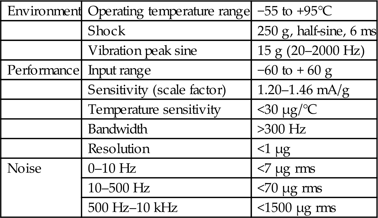
Source: From AlliedSignal Aerospace, accelerometer QA-2000. Units in standard gravity (g).
Example 2
Many humidity sensors have nonlinear behavior. Table 3.2 is an example of the specifications of a typical industrial humidity sensor; RH stands for relative humidity.
Table 3.2
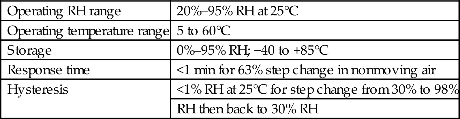
Source: From Amphenol Advanced Sensors, EMD 4000B humidity sensor. Sensitivity curves (impedance vs RH) for various temperatures included in data sheets.
Despite the specified limitations of sensors, a sensing system can be configured in a way that the effect of some of these limitations is eliminated or at least reduced. We consider various possibilities of error-reducing designs in the next section.
3.2 Sensor error reduction techniques
Any sensor system has imperfections, introducing measurement errors. These errors either originate from the system itself (for instance system noise, quantization, and drift) or are due to environmental influences such as thermal, electromagnetic, and mechanical interference. Sensor manufacturers try to minimize such intrinsic errors through proper design of the sensor layout and encapsulation; the remaining imperfections should be given in the data sheets of the sensor. The user (for instance the mechatronic designer) should minimize additional errors that could arise from improper mounting and faulty electronic interfacing. In this section we present some general concepts to minimize or to reduce the effect of the intrinsic errors when applying sensors.
Usually, a sensor is designed to be sensitive to just one specific quantity, thereby minimizing the sensitivity to all other quantities, despite the unavoidable presence of many physical effects. The result is a sensor that is sensitive not only to the quantity to be measured but also in a greater or lesser degree to other quantities; this is called the cross-sensitivity of the device. Temperature is feared most of all, illustrated by the saying that “every sensor is a temperature sensor.”
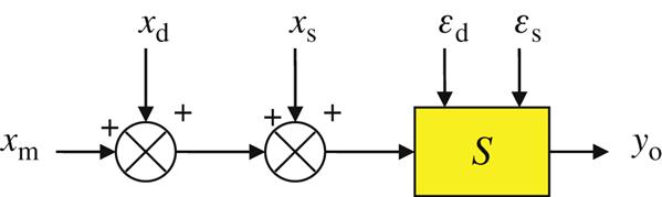
Besides cross-sensitivities, sensors may suffer from many other imperfections. They influence the transfer of the measurement signal and give rise to unwanted output signals. Fig. 3.1 shows a simplified model of a sensor system, with an indication of several error sources. In this figure, xm is the measurement signal and yo the output signal. Additive error signals are modeled as additional input signals: xd and xs represent deterministic and stochastic error signals, respectively. They model all kinds of interference from the environment and the equivalent error signals due to system offset and noise. The error inputs εd and εs represent multiplicative errors: these signals affect the sensitivity of the sensor. For this simplified model, the output signal of a sensor can be written according to Eq. (3.1):
(3.1)
where S is the nominal sensitivity. This model will be used to evaluate various error reduction methods. Some of these methods will reduce mainly additive sensors; others minimize multiplicative errors. Improvement of sensor performance can be obtained through use of a sophisticated design or simply through some additional signal processing. We discuss five basic error reduction methods:
The methods apply not only to sensors but also to other signal-handling systems as amplifiers and signal-transmission systems.
3.2.1 Compensation
Compensation is a simple and effective method to minimize additive errors due to interference signals. The basic idea is as illustrated in Fig. 3.2. In Fig. 3.2A the output of the sensor is y1, which contains unwanted signal components, for instance due to interference xi or offset. From this output a compensation voltage yc is subtracted. The condition for full compensation is yc=Sxi, making yo=Sxm, independent of xi. For correct compensation, the interference signal xi as well as the sensor transfer S should be known. One way to accomplish compensation is by an adjustable compensation signal: at zero input yc is (manually) adjusted to a value for which the output is zero. A more elegant way to compensate is to apply a second sensor, as illustrated in Fig. 3.2B.
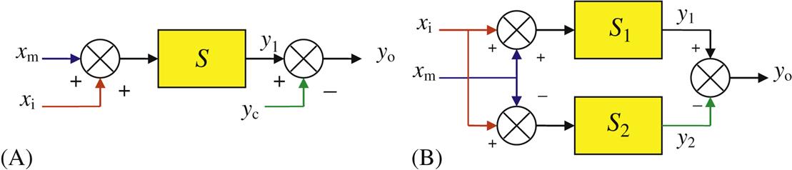
The measurement signal xm is supplied simultaneously to both sensors that have equal but opposite sensitivity to the measurement input (e.g., two strain gauges: one loaded on compressive stress and the other on tensile stress). A minus sign represents the opposite sensitivity of the sensors. The two output signals are subtracted by a proper electronic circuit. Because of the antisymmetric structure with respect to the measurement signal only, many interference signals appear as common output signals and thus are eliminated by taking the difference of the two outputs.
The effectiveness of the method depends on the degree of symmetry of the double sensor or differential sensor structure. From Fig. 3.2 it follows:
(3.2)
where Smk and Sik (k=1, 2) are the sensitivities for the measurement signal and the interference signal, respectively. So, the output signal of the sensor system equals
(3.3)
The sensitivities Sm1 and Sm2 are about equal: Sm1≈ Sm2=Sm, so the output signal becomes
(3.4)
Analogous to the definition of the rejection ratio for differential amplifiers we can define a quality measure for the imbalance of the differential sensor:
(3.5)
a parameter characterizing the system’s ability to distinguish between measurand and interfering signals.
The method is illustrated with a two-active-element Wheatstone measurement bridge (Fig. 3.3).
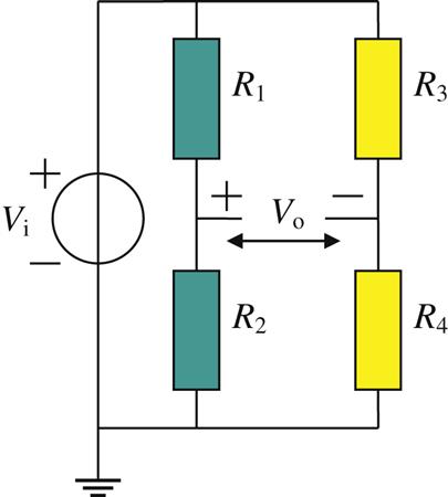
In this half-bridge mode, R3 and R4 are fixed resistances and R1 and R2 are resistive sensors. Their resistance values change with a particular physical quantity as well as an interfering signal, according to:
(3.6)
Here, Smk is the sensitivity of sensor k (k=1, 2) to the measurand (for instance deformation), and Sik is the sensitivity to the interference signal (for instance temperature). Note that in this system the sensor resistance is just R at a particular initial value of the measurand and at zero interference. Assuming both sensor parts experience the same measurement signal and have equal but opposite sensitivities to the measurand, the bridge output voltage satisfies, approximately, the equation:
(3.7)
If both sensor parts have equal sensitivity to interference (by a symmetric sensor design) and both sensor parts experience the interference equally, the error term in Eq. (3.7) is zero, and the interference is completely eliminated. Eq. (3.7) is useful to make a quick assessment of the error due to asymmetry, relative to the measurement signal.
Example
The resistors R1 and R2 in Fig. 3.3 are strain gauges with strain sensitivity Sm=K (gauge factor) and t.c. α (K−1). The measurement signal is the relative deformation or strain Δl/l; the interference signal is a change in temperature Θ. So, the transfer of this bridge is
(3.8)
where ΔΘ is the temperature difference between the two sensor parts and Δα is the difference in temperature sensitivity. In a proper design both sensor parts should have equal temperature and equal temperature sensitivity, over the whole operating range.
3.2.2 Feedback methods
Feedback is an error reduction method originating from the early amplifiers with vacuum tubes. Their unstable operation was a real problem until the application of feedback [6], which reduces in particular multiplicative errors. Fig. 3.4A shows the general idea. The sensor has a nominal transfer S, but due to multiplicative interference it has changed to S(1+εi). The feedback is accomplished by an actuator with an inverse transduction effect and a transfer k. From classical control theory, the error reduction factor can easily be found. The transfer of the total system, Sf, is given by
(3.9)
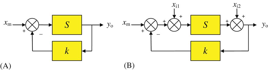
A relative change dS in the sensor transfer S causes a relative change dSf in Sf according to:
(3.10)
In an appropriate feedback system design, kS![]() 1. So, the relative error in the forward part is reduced by a factor equal to the loop gain S·k of the system. The penalty for this improvement is a reduction of the overall sensitivity with the same factor.
1. So, the relative error in the forward part is reduced by a factor equal to the loop gain S·k of the system. The penalty for this improvement is a reduction of the overall sensitivity with the same factor.
Feedback also reduces additive interference signals, in a degree that depends on the point of injection in the system. Two cases are discussed in Fig. 3.4B. The output due to two interfering signals xi1 and xi2 equals:
(3.11)
Obviously, signals entering at the input of the system are reduced by feedback as much as the measurement signal (so the SNR is not better). Interfering signals injected at the output of the sensing system are reduced by a factor S more than the measurement signal, so the SNR is increased by the same amount.
Feedback reduces errors in the forward signal path: the transfer is mainly determined by the feedback path. Nonlinearity in the forward path (for instance due to a nonlinear sensor characteristic) is also reduced, provided a linear transfer of the feedback element. Prerequisites for an effective error reduction are as follows:
The application of this method to sensors requires a feedback element with a transfer that is the inverse of the sensor transfer. Imperfections of the sensor are reduced; however, the demands on the actuator are high. The method is illustrated with an example of a capacitive accelerometer system in which two error reduction methods are combined: compensation by a balanced sensor construction and feedback by an inverse transducer (Fig. 3.5).
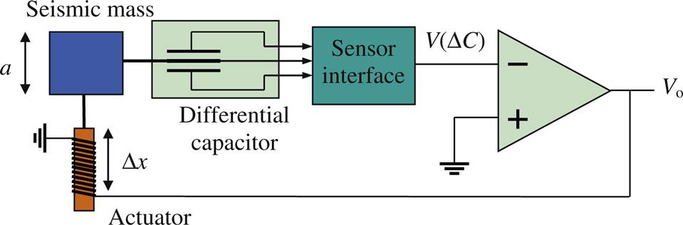
A displacement of the seismic mass m results in a capacitance difference ΔC; this value is converted to a voltage, which is compared with a reference value (here this value is 0). The amplified voltage difference is supplied to an electromagnetic actuator that drives the mass back toward its initial position. When properly designed, the system reaches a state of equilibrium in which the applied inertial force is compensated by the electromagnetic force from the actuator. The current required to keep equilibrium is a measure for the applied force or acceleration.
A more detailed model of this system, for instance for stability analysis, is depicted in Fig. 3.6. All transduction steps are visualized in separate blocks. Obviously, the feedback is performed in the mechanical domain by counteracting the inertial force Fi with the electromagnetic force Fa of the actuator.
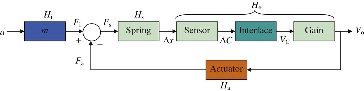
The transfer function of the whole system can easily be derived from this model and is given in Eq. (3.12):
(3.12)
In this equation, Hi is the transfer from applied acceleration a to inertial force Fi. Hs is the transfer of the mechanical spring: from force to displacement Δx. The transfer of the electrical system (capacitive sensor, electronic interface, and amplifier together) is He. Finally, Ha is the transfer of the actuator. For ![]() , the transfer function of the total sensor system becomes:
, the transfer function of the total sensor system becomes:
(3.13)
Indeed this is independent of the spring stiffness, the sensor transfer, the interface, and the gain of the amplifier, according to the feedback principle. In equilibrium, the mass is at its center position. Hence, no particular demands have to be made on the spring, the sensor, and the interface circuit; the only requirement is a small zero error. Actually, the requirements with respect to the sensor quality have been transferred to those of the actuator. The system transfer depends only on the seismic mass m and the actuator transfer Ha.
Feedback may also improve the dynamic performance of the sensor. Assume the sensor in Fig. 3.6 is a mass-spring system described by the general second order (complex) transfer characteristic
(3.14)
with z the damping and ω0 the natural (undamped) frequency or resonance frequency of the system. Substitution in Eq. (3.9) results in the transfer of the system with feedback:
(3.15)
with a new damping factor ![]() and a new natural frequency
and a new natural frequency ![]() . Obviously, the resonance frequency is increased by a factor
. Obviously, the resonance frequency is increased by a factor ![]() and the damping is decreased with the same factor: the system has become faster by feedback.
and the damping is decreased with the same factor: the system has become faster by feedback.
The principle is also applicable for other measurands, for instance pressure. Many pressure sensors are based on a flexible membrane that deforms when a pressure difference is applied. Usually, this deformation is measured by some displacement sensor, providing the output signal. The effect of the strong nonlinear response of the membrane can be eliminated by feedback, using a (linear) actuator in the feedback path [7]. There are various sensors on the market that are based on the feedback principle. Some of them will be discussed in later chapters.
3.2.3 Filtering
Error signals can be reduced or avoided by filtering, to be performed either in the domain of the interfering signal (prior to transduction) or in the electrical domain (after transduction).
3.2.3.1 Filtering prior to transduction
The unwanted signals may be kept outside the sensor system by several filtering techniques, depending on the type of signal. Sometimes the technique is referred to as shielding. We briefly review some causes and the associated reduction methods:
- • Electric injection of spurious signals, through a capacitive connection between the error voltage source and the system input; to be avoided by a grounded shield around the sensor structure and the input leads. The capacitively induced current flows directly to ground and does not reach the input of the sensor.
- • Magnetically induced signals by a time-varying magnetic flux through the loop made up by the input circuit; cannot only be reduced by a shield made up of a material with a high magnetic permeability but also by minimizing the area of the loop (leads close to each other or twisted).
- • Changes in environmental temperature; thermal shielding (an encapsulation with high thermal resistance or a temperature-controlled housing) reduce thermal effects.
- • Unwanted optical input (from lamps, the sun) can be stopped by optical filters; many filter types are available on the market. Measurand and interferences should have a substantial difference in wavelength.
- • Mechanical disturbances (e.g., shocks and vibrations) are reduced by a proper mechanical construction with elastic mounting and performing suitable damping of the vibrations.
3.2.3.2 Filtering after transduction
In case the interfering signals are of the same type (in the same signal domain) as the measurand itself, error reduction is accomplished with filters based on differences in particular properties of the signals. For electrical signals, the distinguishing property is the frequency spectrum. Electrical interfering signals with a frequency spectrum different from that of the measurand can easily be filtered by electronic filters (Appendix C). If they have overlapping frequency spectra, this is not or only partially possible. A solution to this problem is to modulate (if possible) the measurement signal prior to transduction, to create a sufficiently large frequency difference, enabling effective filtering in the electrical domain (see Section 3.2.4).
3.2.4 Modulation
Modulation of the measurement signal is a very effective way to reduce the effect of offset errors and noise. We shortly review the basics of amplitude modulation and demodulation, and show that this combination behaves as a narrow band-pass filter process.
Modulation is a particular type of signal conversion that makes use of an auxiliary signal, the carrier. One of the parameters of this carrier signal is varied analogously to the input (or measurement) signal. The result is a shift of the complete signal frequency band to a position around the carrier frequency. Due to this property, modulation is also referred to as frequency conversion.
A very important advantage of modulated signals is their better noise and interference immunity. In measurement systems, modulation offers the possibility of bypassing offset and drift from amplifiers. Amplitude modulation is a powerful technique in instrumentation to suppress interference signals; therefore we confine to amplitude modulation only.
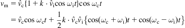
A general expression for an AM signal with a sinusoidal carrier ![]() modulated by an input signal vi(t) is as follows:
modulated by an input signal vi(t) is as follows:
(3.16)
where ωc is the frequency of the carrier, and k is a scale factor determined by the modulator. Suppose the input signal is a pure sine wave:
(3.17)
The modulated signal is as follows:
(3.18)
 (3.18)
which shows that this modulated signal has three frequency components: one with the carrier frequency (ωc), one with a frequency equal to the sum of the carrier frequency and the input frequency (ωc+ωi), and one with the difference between these two frequencies (ωc−ωi). Fig. 3.7A shows an example of such an AM signal. The input signal is still recognized in the “envelope” of the modulated signal, although its frequency component is not present.
When the carrier is modulated by an arbitrary input signal, each of the frequency components in its spectrum (Fig. 3.7B) produces two new components, with the sum and the difference frequency. Hence, the whole frequency band is shifted to a region around the carrier frequency (Fig. 3.7C). These bands at either side of the carrier are called the side bands of the modulated signal. Each side band carries the full information content of the input signal. The AM signal does not contain low-frequency components anymore. Therefore it can be amplified without being disturbed by offset and drift (which are low-frequency signals). If such frequencies appear anyway in the amplified modulated signal, they can easily be removed by a high-pass filter.
There are many ways to modulate the amplitude of a carrier signal. We discuss three methods: the multiplying modulator, the switch modulator, and the bridge modulator.
3.2.4.1 Multiplier as modulator
Multiplication of two sinusoidal signals vc and vi (carrier and input) results in an output signal:
(3.19)
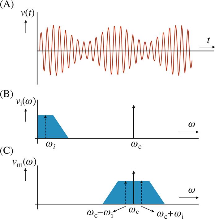
with K the scale factor of the multiplier. This signal contains only the two-side band components and no carrier; it is called an AM signal with suppressed carrier. For arbitrary input signals, the spectrum of the AM signal consists of two (identical) side bands without carrier. Fig. 3.8A shows an example of such an AM signal. Note that the “envelope” is not identical to the original signal shape anymore. Furthermore, the AM signal shows a phase shift in the zero crossings of the original input signal (Fig. 3.8B).
3.2.4.2 Switch modulator
In the switch modulator, the measurement signal is periodically switched on and off, a process that can be described by multiplying the input signal with a switch signal s(t), being 1 when the switch is on and 0 when it is off (Fig. 3.9).
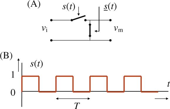
To show that this product is indeed a modulated signal with side bands, we expand s(t) into its Fourier series:
(3.20)
with ω=2π/T and T the period of the switching signal. For a sinusoidal input signal with frequency ωi, the output signal contains sums and differences of ωi and each of the components of s(t).
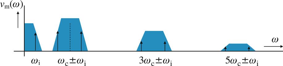
This modulation method produces a large number of side band pairs, positioned around odd multiples of the carrier frequency (ωc, 3ωc, 5ωc, …), as shown in Fig. 3.10. The low-frequency component originates from the multiplication by the mean of s(t) (here ½). This low-frequency component and all components with frequencies 3ωc and higher can be removed by a filter. The resulting signal is just an AM signal with suppressed carrier.
Advantages of the switch modulator are its simplicity and accuracy: the side band amplitude is determined only by the quality of the switch. A similar modulator can be achieved by periodically changing the polarity of the input signal. This is equivalent to the multiplication by a switch signal with zero mean value; in that case there is no low-frequency band as in Fig. 3.10.
The absence of DC and low-frequency components considerably facilitates the amplification of modulated signals: offset, drift, and low-frequency noise can be kept far from the new signal frequency band. When very low voltages must be measured, it is recommended to modulate these prior to any other analog signal processing that might introduce DC errors.
3.2.4.3 Measurement bridge as modulator
The principle of the bridge modulator is illustrated with the resistance measurement bridge or Wheatstone bridge of Fig. 3.11.
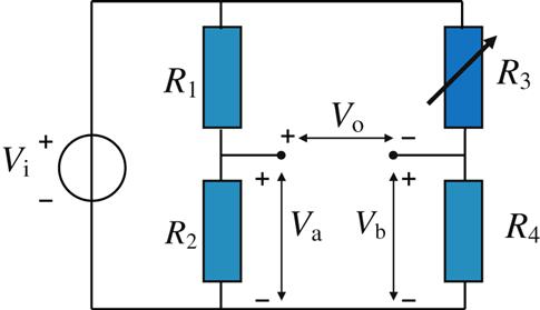
The bridge is connected to an AC signal source Vi. This AC signal (usually a sine or square wave) acts as the carrier. In this example we consider a bridge with only one resistance (R3) that is sensitive to the measurand. Assuming equal values of the three other resistances, the signal Va is just half the carrier, whereas Vb is an AM signal: half the carrier modulated by R3. The bridge output Vo is the difference between these two signals, so it is an AM signal with suppressed carrier.
This output can be amplified by a differential amplifier with high gain; its low-frequency properties are irrelevant; the only requirements are a sufficiently high bandwidth and a high common mode rejection ratio (CMRR) for the carrier frequency to accurately amplify the difference Va−Vb.
Modulation techniques also apply to many nonelectric signals. An optical signal can be modulated using a LED or laser diode. If the source itself cannot be modulated, optical modulation can be performed by, for instance, a chopping wheel, as is applied in many pyroelectric measurement systems. Also, some magnetic sensors employ the modulation principle. Special cases are discussed in subsequent chapters.
3.2.5 Demodulation
The reverse process of modulation is demodulation (sometimes called detection). Looking at the AM signal with carrier (for instance in Fig. 3.7), we observe the similarity between the envelope of the amplitude and the original signal shape. An obvious demodulation method would therefore be envelope detection or peak detection. Clearly, envelope detectors operate only for AM signals with carrier. In an AM signal without carrier, the envelope is not a copy of the input anymore. Apparently, additional information is required with respect to the phase of the input, for a full recovery of the original waveform.
An excellent method to solve this problem, and which has a number of additional advantages, is synchronous detection. This method consists of multiplying the AM signal by a signal having the same frequency as the carrier. If the carrier signal is available (as is the case in most measurement systems), this synchronous signal can be the carrier itself.
Assume a modulated sinusoidal input signal with suppressed carrier:
(3.21)
This signal is multiplied by a synchronous signal with a frequency equal to that of the original carrier, and a phase angle φ. The result is as follows:
(3.22)
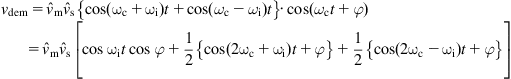 (3.22)
With a low-pass filter, the components around 2ωc are removed, leaving the original component with frequency ωi. This component has a maximum value for φ=0, that is, when the synchronous signal has the same phase as the carrier. For φ=π/2 the demodulated signal is zero, and it has the opposite sign for φ=π. This phase sensitivity is an essential property of synchronous detection.
Fig. 3.12 reviews the whole measurement process in terms of frequency spectra. The starting point is a low-frequency narrow band measurement signal (A). This signal is modulated and subsequently amplified. The spectrum of the resulting signal is depicted in (B), showing the AM spectrum of the measurement signal and some additional error signals introduced by the amplifier: offset (at DC), drift and 1/f noise (LF), and wide band thermal noise.
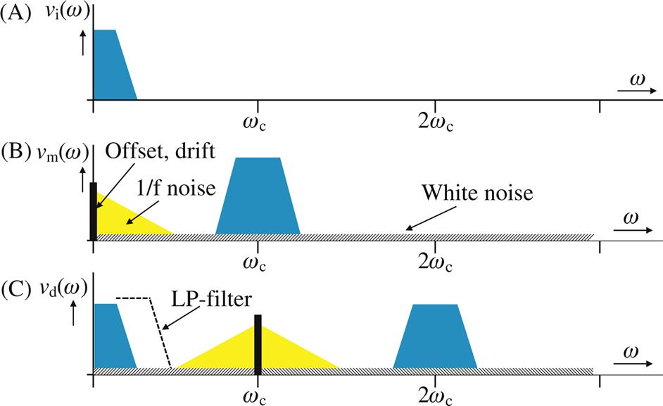
Fig. 3.12C shows the spectrum of the demodulated signal. By multiplication with the synchronous signal, all frequency components are converted to a new position. The spectrum of the amplified measurement signal folds back to its original position, and the LF error signals are converted to a higher frequency range. A low-pass filter removes all components with frequencies higher than that of the original band.
An important advantage of this detection method is the elimination of all error components that are not in the (small) band of the modulated measurement signal. If the measurement signal has a narrow band (slowly fluctuating measurement quantities), a low cut-off frequency of the filter can be chosen. Hence, most of the error signals are removed, and a remarkable improvement of the S/N ratio is achieved, even with a simple first-order low-pass filter.
The low-pass filter with bandwidth B, acting on the demodulated signal, is equivalent to a band-pass filter acting on the modulated signal (around the carrier). This means that the effective bandwidth is 2B. The selectivity of a band-pass filter is expressed with the quality factor Q, defined as the ratio between its central frequency fc and the (−3 dB) bandwidth B. So the synchronous detector can be conceived as a band-pass filter with quality factor equal to fc/B. If, for example, the measurement signal has a bandwidth of 0.5 Hz, then the cut-off frequency of the low-pass filter is also set to 0.5 Hz. Suppose the carrier frequency is 4 kHz, then the effective quality factor of the synchronous detector is 4000. Active band-pass filters can achieve Q-factors of about 100 at most, so synchronous detection offers a much higher selectivity compared to active filtering.
3.2.6 Correction methods
An erroneous sensor signal can be corrected if knowledge about the causes of the errors or the value of the errors is available. Two different strategies can be distinguished:
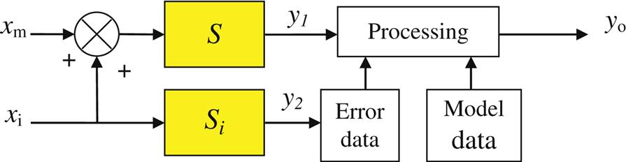
In the first class of strategies, correction is performed while leaving the sensor unaltered. Fig. 3.13 shows the general configuration for two approaches. In the model-based approach, the sensor signal is corrected based on prior knowledge about the origin of the error, for instance nonlinearity or a calibration curve, stored in a look-up table. If the errors are unknown (interference), the error signal could be measured separately by additional sensors. The output of these sensors is used to correct the original sensor signal. The method is straightforward but requires additional sensors, at least one for each type of interference.
Dynamic correction involves a particular sensor design. Basically, the method involves a series of measurements of the same quantity, in such a way as to eliminate the errors by postprocessing. This can be done in various ways, according to the type of quantity and error:
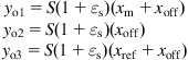
The first method is illustrated in Fig. 3.14. Additive errors are represented by the signal xoff. Multiplicative errors due to the interfering signal xs are represented by the relative error εs. Alternately, the input of the system is connected to the measurand (yielding an output yo1), to “ground” (giving output yo2) and to a reference (resulting in the output yo3).
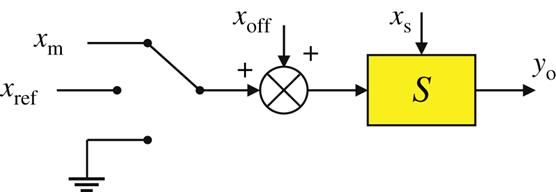
The three system outputs are as follows:
(3.23)
 (3.23)
From these equations, the measurand can be calculated as follows:
(3.24)
Offset and scale errors are completely eliminated if the errors do not change during the sequence of the three measurements. The method requires a reference of the measurand type as well as a possibility to completely isolate the input from the measurand to find the offset error contribution. For most electrical quantities, like voltage, capacitance, and resistance, this is quite an easy task. This is not the case for many other physical quantities: repetitively short-circuiting the input of a magnetic field sensor or a force sensor. For instance, without removing the measurand itself requires complicated and therefore impractical shielding techniques.
All sensor systems suffer from offset and drift, which hampers the measurement of small, slowly varying signals. Modulation, as discussed earlier, is a very effective way to eliminate offset. However, modulation of the input signal is not always possible. An alternative way to reduce offset is flipping the directivity of the sensor, without changing the sign and value of the offset. Clearly, the method can only be applied for sensors that are sensitive to the direction of the input quantity (which should be a vector).
Flipping is performed either by changing the carrier signal in modulating sensors or by rotation of the sensor itself. An example of a modulating sensor (Chapter 2: Sensor fundamentals) is the Hall sensor for the measurement of magnetic field strength (Chapter 6). This is a modulating type sensor because the output is proportional to both the input signal and an auxiliary signal, in this case a DC bias current. Assuming the offset being independent of the bias, the offset reduction follows from Eq. (3.25), where xc is the carrier signal that is flipped between two successive measurements.
(3.25)
Obviously, the difference between the two outputs is proportional to the input signal and offset independent. When the sensor is not of the modulating type, the same effect is obtained by just rotating the sensor [8]. Since this mechanical flipping requires some moving mechanism, the method is restricted to low-frequency applications.
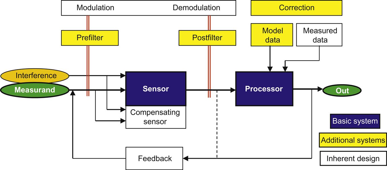
All error reduction methods discussed in this section are illustrated schematically in Fig. 3.15. In this scheme, the basic signal flow is shown in dark color. The performance of a noncompensated sensor can be improved by adding error-reducing systems, for instance filters, modulators, and correction circuitry (halftone). When designing a sensor system, other techniques are worth consideration, for instance the inclusion of a compensating sensor in a balanced configuration, or the incorporation of a modulator whenever possible (white parts in Fig. 3.15). During the design process of a particular sensing system, it is recommended to consider all these possibilities, in connection to the possible occurrence of errors.