
Resistive sensors
Abstract
The sensors presented in this chapter are all based on resistive effects: they behave as an electrical resistor whose resistance is affected by a particular physical quantity. Quantities that can be measured using resistive effects are temperature (thermistors and metal thermometers), light (light-dependent resistor), deformation (piezoresistors), and magnetic field strength (magnetoresistors). By a special construction or material choice, resistors can be made useful for sensing other quantities, for instance force, torque, pressure, distance, angle, velocity, and acceleration.
After a brief discussion on resistance and resistivity this chapter treats successively potentiometric sensors, strain gauges, and piezoresistive and magnetoresistive sensors. Further, some thermal and optical sensors based on resistive effects are reviewed. This chapter also includes sections on interface circuits for potentiometers and strain gauges and on particular applications of resistive sensors.
Keywords
Resistivity; potentiometric sensors; strain gauges; gauge factor; force–torque sensors; piezoresistivity; magnetoresistivity; thermal resistivity; Pt100; thermistor; LDR; applications and embedded interfacing
In this chapter, we discuss sensors based on resistive effects. These sensors behave as an electric resistor whose resistance is affected by a particular physical quantity. The resistance may change according to a change in material properties, a modification of the geometry or a combination of these. Quantities that can easily be measured using resistive effects are temperature (thermistors and metal thermometers), light (LDR or light-dependent resistor), deformation (piezoresistors), and magnetic field strength (magnetoresistors). By a special construction or material choice, resistors can be made useful for sensing various quantities, for instance force, torque, pressure, distance, angle, velocity, and acceleration.
After having defined resistance and resistivity, we discuss successively potentiometric sensors, strain gauges, piezoresistive, and magnetoresistive sensors. Further, some thermal and optical sensors based on resistive effects are reviewed. The last section presents a number of applications of resistive sensors, including the interfacing.
4.1 Resistivity and resistance
The electrical conductivity σ (the inverse of electrical resistivity ρ) is defined as the ratio between current density J (A/m2) and electric field strength E (V/m):
Conductivity is a pure material property: it does not depend on shape or size of the device (skin effect and thin-layer effects are disregarded here). In this section, all materials are assumed to be homogeneous. The resistance between the endpoints of a bar with length l and constant cross-section A equals:
The parameter l is used to create distance sensors and angular displacement sensors: these sensors are called potentiometric sensors and are discussed in Section 4.2. Strain gauges are based on changes in l/A (applied in force and pressure sensors, Section 4.3), while the parameter ρ is the property of interest in piezoresistive, magnetoresistive, thermoresistive, and optoresistive sensors (Sections 4.4–4.7). Table 4.1 presents an overview of the various resistive sensors discussed in this chapter.
Table 4.1
4.2 Potentiometric sensors
4.2.1 Construction and general properties
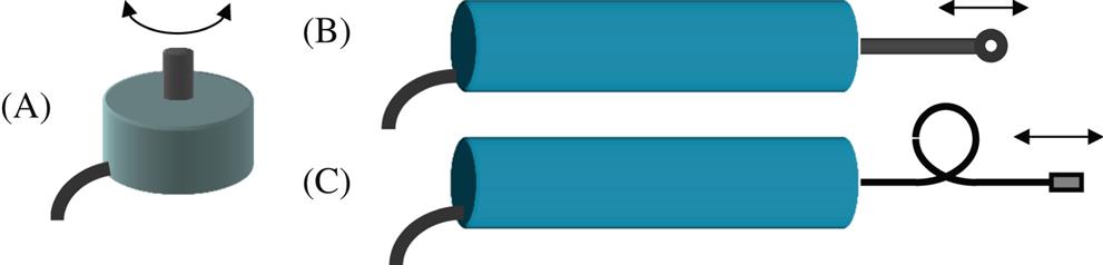
Potentiometric displacement sensors can be divided into linear and angular types, according to their purpose and associated construction. A potentiometric sensor consists of a (linear or toroidal) body which is either wire wound or covered with a conductive film. A slider (or wiper) can move along this conductive body, acting as a movable electrical contact. The connection between the slider and the object of which the displacement should be measured is performed by a rotating shaft (angular potentiometers), a moving rod, an externally accessible slider (sledge type), or a flexible cable that is kept stretched during operation. Fig. 4.1 shows a schematic view of some of these constructions. In all cases the resistance wire or film and the wiper contacts should be properly sealed from the environment to minimize mechanical damage and corrosion. This is an important issue when applied in mechatronic systems that operate in harsh environments. Robust potentiometers have a stainless steel shaft or rod, and a housing of, for instance, anodized aluminum. The moving parts of the potentiometer are provided with bearings, to minimize the mechanical force needed to initiate movement of the slider and minimizing wear.
Potentiometric sensors are available in a wide variety of ranges. Linear types vary in length from several millimeters up to a few meters, angular types have ranges from about π/2 rad up to multiples (2–10) of 2π (multiturn potentiometers), achieved by built-in gears or a spindle construction.
The specification of potentiometric sensors is standardized by the Instrument Society of America [1]. We list here the major items, in a short formulation. VR stands for voltage ratio, that is, the ratio between the wiper voltage and the full voltage across the resistor:
- • range (linear distance or angle)
- • linearity (in %VR over total range)
- • hysteresis (in %VR over specified range)
- • resolution (average and maximum)
- • mechanical travel (movement from one stop to the other)
- • electrical travel (portion of mechanical travel during which an output change occurs)
- • operating temperature
- • temperature error (in %VR per °C or in %VR over a quarter of the full range)
- • frequency response (at given amplitude)
- • cycling life (number of cycles at 1/4 of the maximum frequency)
- • storage life (month, year)
- • operating force or torque (break-out force or torque) to initialize movement
- • dynamic force or torque (to continuously move the shaft after the first motion has occurred)
- • shaft overload (at the extremities of the mechanical travel; without damage or degradation)
- • shaft axial misalignment
A manufacturer should mention all these specifications in the data sheets of the device. Table 4.2 lists the main specifications for various types of potentiometers. Besides the specifications listed in this table, many other parameters should be considered when using a potentiometer as displacement sensor, in particular in mechatronics applications. Some of them are listed below:
- • maximum allowable force or torque on the wiper;
- • minimum force or torque to move the wiper; typical starting torque is 0.1 Ncm, for a “low-torque” potentiometer this can be less than 0.002 Ncm and for a robust type as high as 10 Ncm;
- • maximum (rotational) wiper speed (usually about 1000 rpm);
- • maximum voltage across the resistor (typically 10 V);
- • maximum current through the wiper contact (typically 10 mA).
Table 4.2

4.2.2 Electrical characteristics
Potentiometric displacement sensors can electrically be connected in two different ways: the potentiometric wiring and the rheostat wiring (Fig. 4.2). In rheostat mode the device acts just as a variable resistor (two terminal); the potentiometer mode is suitable for voltage division (two-port configuration; Fig. 4.5).
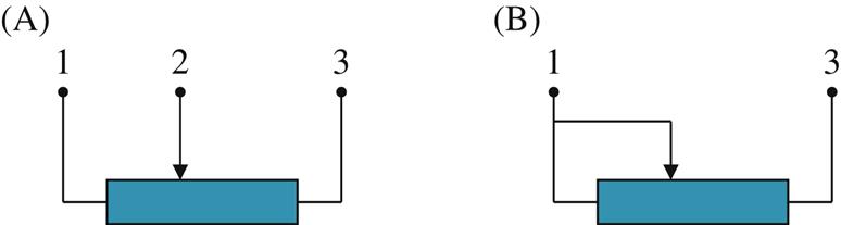
The VR of a potentiometer equals R12/R13 which, for an ideal potentiometer, is equal to x/L, with L the electrical stroke and x the distance between the start position and the wiper position (Fig. 4.3).

Nonlinearity and resolution are the main causes of a deviation from this ideal transfer. A linear relationship between position and wiper voltage requires a wire or film with homogeneous resistivity over the whole range. The intrinsic nonlinearity can be as good as 0.01% (see Table 4.2). Improper interfacing may introduce additional nonlinearity, as will be explained in Section 4.2.3.
The position resolution of a wire-wound potentiometer is set by the number of turns n. With R the total resistance the resistance of a single turn amounts ΔR=R/n. As the wiper steps from one turn to the next, the VR changes leap-wise with an amount of 1/n when the wiper moves continuously (Fig. 4.4A); hence the resolution equals ΔR/R=1/n. At wiper position on top of turn i, VR equals i/n; on top of the next turn, it increases to (i+1)/n. Actually the wiper may short circuit one turn when positioned just between two windings (Fig. 4.4B). In those particular positions the total resistance drops down to (n−1)ΔR, hence VR=i/(n−1), which is slightly more than i/n, as shown in Fig. 4.4C.

The resolution can be increased (without change of outer dimension) by reducing the wire thickness. However, this degrades the reliability because a thinner wire is less wear resistant. The resolution of a film potentiometer is limited by the size of the carbon or silver grains that are impregnated in the plastic layer to turn it into a conductor. The grain size is about 0.01 μm; the resolution is about 0.1 μm at best.
4.2.3 Interfacing
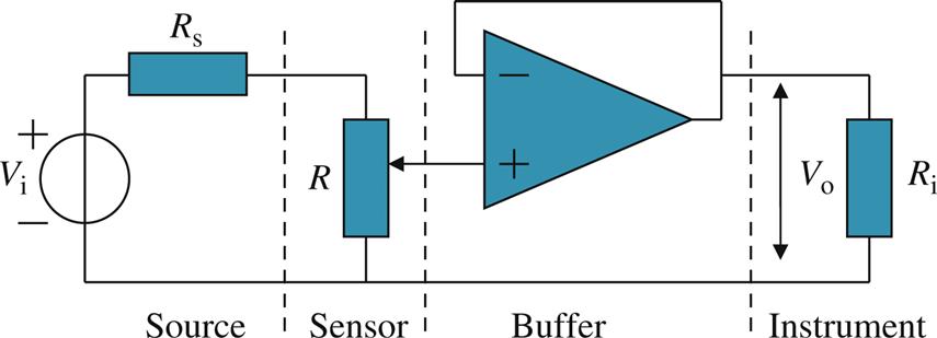
The interfacing of a potentiometric sensor is essentially simple (Fig. 4.5).
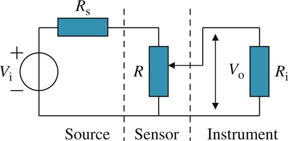
To measure the position of the wiper the sensor is connected to a voltage source Vi with source resistance Rs; the output voltage on the wiper, Vo, is measured by an instrument with input resistance Ri. Ideally the voltage transfer Vo/Vi equals the VR. Due to the presence of a source resistance and load resistance, the transfer might differ from the VR. We will calculate the error introduced by both these effects.
First assume Rs=0 and Ri→∞; under this condition the output voltage of the sensor satisfies Eq. (4.3) for a linear potentiometer or Eq. (4.4) for an angular potentiometer:
where L is the total electrical length and αmax is the maximum electrical angle. The sensitivity of a linear sensor is
and apparently is independent of the resistance R and proportional to the source voltage. The sensitivity can be increased by increasing the source voltage. Obviously the maximally permissible power ![]() should be kept in mind. When ambient temperature increases, the maximum allowable dissipation drops; it is wise to carefully check the data sheets on this aspect.
should be kept in mind. When ambient temperature increases, the maximum allowable dissipation drops; it is wise to carefully check the data sheets on this aspect.
Instability of Vi results in an output change that is indiscernible to displacement. The effect is maximal for x=L, so a stability criterion for Vi is
where Δxm is the smallest detectable displacement. Otherwise stated the stability of the source voltage should be better than the resolution of the potentiometer.
A nonzero value of the source resistance introduces a scale error. For Rs≠0 and Ri→∞ the sensor transfer is
Hence the sensitivity is reduced by an amount Rs/R with respect to the situation with an ideal voltage source (Rs=0).
A load resistance Ri results in an additional nonlinearity error. Now assuming Rs=0, the voltage transfer is
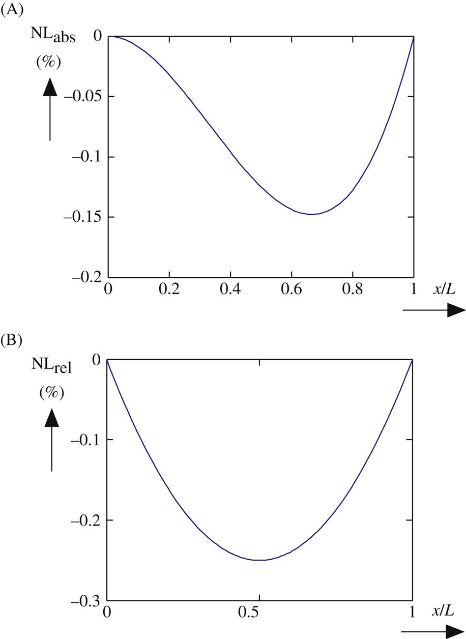
The approximation is valid when R/Ri![]() 1. The end-point linearity error (see Section 3.1), in this case the deviation from the ideal transfer x/L, amounts:
1. The end-point linearity error (see Section 3.1), in this case the deviation from the ideal transfer x/L, amounts:
The maximal error is (−4/27)(R/Ri), occurring at x/L=2/3. This error adds up to the intrinsic nonlinearity error of the sensor, which is due to unevenly winding or inhomogeneity of the wire or film material. The relative nonlinearity is
from which follows a maximum relative deviation of (−1/4)(R/Ri), occurring at the position x/L=0.5 (midway between the end points). Both errors are proportional to the resistance ratio R/Ri. Fig. 4.6 shows the absolute and relative nonlinearity error for the case R/Ri=1%. In this case the (absolute) nonlinearity is about 0.15%. If, for example, the absolute nonlinearity due to loading should be less than 0.05% over the full range of the potentiometer, then the minimum value for the load resistance should be 300 times that of the potentiometer.
Additional nonlinearity due to a possibly low input resistance of the measurement instrument can be circumvented by inserting a voltage buffer between the wiper and the measurement instrument, as shown in Fig. 4.7. Such a buffering alleviates the requirements on the input resistance of the readout circuit.
The influence of source voltage changes can be reduced by applying a ratio method, as is illustrated in Fig. 4.8. The transfer of the analog to digital converter (ADC) is Va=Gn×Vr, where Gn is the binary coded fraction between 0 and 1. Since the reference voltage of the ADC equals the voltage across the potentiometer, from Eq. (4.3) it follows Gn=x/L which, in the ideal case, does not depend on Vi. The ADC output can be directly processed by a computer.

Interfacing a potentiometer in embedded systems can be performed without external components. This is illustrated in Fig. 4.9 where a potentiometer is directly interfaced to an Arduino Board. In this case the microcontroller's supply voltage is used as source for the sensor. When no other (heavy) loads are attached to the same source, this is a viable solution. In the default configuration the ADC of the board has the supply voltage as reference. The input impedance is high enough compared to the sensor's resistance to be neglected. In this case the angle of the potentiometer will be linearly mapped to the 0–5.0 V input range. Using the conventional implementation of the ADC functions in Arduino (i.e., int inputvalue=analogRead(A0)), the angle of rotation 0–270° is mapped to a value between 0 and 1023. A simple code example for recording and plotting the angle is described in Appendix D.

4.2.4 Contact-free potentiometers
Gradually film potentiometers grow in popularity over wire-wound types, because of higher resolution and a better resistance against moisture. However, one important disadvantage still remains: wear due to the sliding contact of the wiper. To get around this drawback, contact-free potentiometers have been developed. In the design presented in Ref. [2] the slider has been replaced by a floating electrode; the resistance track acts as counter electrode of the capacitor. Obviously, wear is minimized in this way.
The basic construction of potentiometers with capacitive readout is shown in Fig. 4.10A. The floating wiper is capacitively coupled to the resistance track and a conductive return track. A voltage Vi is connected across the resistance track and the return track is linked to the interface circuit.
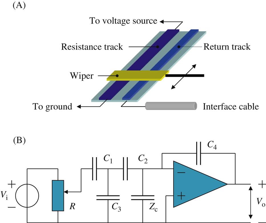
Fig. 4.10B shows the electric circuit model of the sensor and a simple readout circuit: C1 is the capacitance between the resistance track and the wiper; C2 is the capacitance between the return track and the wiper; C3 is the stray capacitance between wiper and ground. The inverting input of the operational amplifier is virtually at ground potential (see Appendix C, Basic interface circuits), so the voltage across the cable impedance Zc is zero. This makes the transfer of the device independent of the cable impedance.
When the stray capacitance C3 is small compared with C1 and C2, the voltage transfer of this circuit is given by
where Cw=C1+C2 and Rp is the parallel resistance of the two parts of the potentiometer. The latter varies with the wiper position; its maximum value occurs when the wiper is in the center position of the potentiometer, and equals R/4. The transfer function shows a first-order low-pass behavior, characterized by the time constant RpCw. Since the wiper capacitance Cw is almost constant, the sensor’s time constant varies with the wiper position; halfway through the electrical stroke the system has the lowest bandwidth. For low frequencies of the source voltage the output voltage is directly proportional to the VR of the potentiometer, hence proportional to the displacement of the wiper. The low-frequency gain of the interface circuit amounts Cw/C4 and can be given a specified value by a proper choice of C4.
Note that the feedback capacitor C4 should be shunted by a resistance to prevent the operational amplifier from running into saturation due to integration of its offset voltage and bias current (see also Appendix C.6, Basic interface circuits). Together with C4, this resistance introduces another time constant, so the associated cut-off frequency should be chosen well above the frequency of the voltage source.
Similar to the conventional types the nonlinearity of the contact-free potentiometer is determined by the inhomogeneity of the resistance track and is, therefore, not much better than the traditional types. However, the transfer characteristic is somewhat smoothed due to the extension of the floating wiper: small local irregularities are averaged out.
Contrary to this contact-free solution using capacitive coupling, also film potentiometers with a resistive polymer exist (see Fig. 4.11) which use pressure to make contact between the wiper and the resistance track. In this case the wiper consists of a long conductive track which extends to the full length of the resistance track. Pressure applied by touch, i.e., through a human finger or mechanical device, will make contact between wiper and track at a certain spot. These devices also avoid the sliding friction normally associated with mechanical wipers.

4.2.5 Applications of potentiometers
Potentiometric sensors are very popular devices because of the relatively low price and easy interfacing. Evidently linear and angular potentiometers can be used as sensors for linear displacement and angle of rotation, respectively. For this application the construction element of which the displacement or rotation should be measured is mechanically coupled to the wiper. If the range of movement does not match that of the potentiometer, a mechanical transmission can be inserted. However, this might introduce additional backlash and friction, reducing the accuracy of the measurement. Proper alignment of object and sensor is extremely important here.
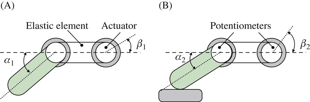
Potentiometers are widely used in all kind of mechatronic systems to obtain information about angular positions of rotating parts. When small dimensions should be combined with a high resolution, potentiometers may be preferred over the popular optical encoders (see Chapter 7, Optical sensors). For example, controlling a multifingered robotic hand requires several angular position sensors located at the joints of the fingers. Potentiometers have been considered as one of the possibilities to achieve this goal (see, for instance, Ref. [3]). Fig. 4.12 shows how potentiometers, in combination with an elastic element, are used to measure joint angles α and β, from which follows the touch force exerted by the fingertip on an object.
A particular application of a potentiometric sensing device is an angular sensor for knee rotation, described in Ref. [4]. Two nonelastic wires are positioned along the leg, in parallel to the plane of rotation. At one end the wires are connected to each other and both other ends are connected to the sliders of two potentiometers. Springs keep the wires stretched. On bending the free ends show a relative displacement related to the angle of rotation. The potentiometers form a Wheatstone bridge, so only the position difference of the wire ends is measured. The resolution of the measurement is better than 0.1° over a range of 100°.
The use of potentiometers is not restricted to the measurement of linear and angular displacement. They can also be used for the measurement of acceleration, force, pressure, and level. In these cases the measurand is transferred to a displacement by a proper mechanical construction. Combined with a spring a potentiometer can act as a force sensor; with a seismic mass fixed to the slider the construction is sensitive to acceleration. Potentiometric accelerometers are available for ranges up to 10 g, inaccuracy around 2% full scale (FS), and a lateral sensitivity less than 1% (i.e., 1% of the sensitivity along the main axis).
Potentiometers find also application in gyroscopes with spinning rotor. When rotated, the axis of the rotor tends to maintain its original position hence making an angle with the sensor housing in proportion to the angular velocity. Gyroscopes are available in which two angles, roll and pitch, are measured by built-in potentiometers.
Another application is the measurement of level. For this purpose, potentiometers of the type shown in Fig. 4.1C are used. In case of a liquid the one end of the flexible cable is connected to a float and at the other end wound on a drum. When the level is raising or lowering, the drum winds or unwinds; a rotational potentiometer measures the rotation of the drum. In case of a granular material the measurement is usually performed intermittently: a weight on a flexible cable drops down until it reaches the top level of the material. The sudden change in the cable tension marks the distance over which the cable has been unrolled.
A potentiometer-like sensor for measuring tilt is presented in Ref. [5]. Although not a potentiometer in the usual sense, it functions in a similar way. The resistive material is an electrolytic solution residing in a micromachined cavity, and the three electrodes are fixed to the walls: two at both ends of the cavity and one in the middle. In horizontal position the resistances between the middle electrode and both end electrodes are equal, but when tilted the resistance ratio varies according to the angle of rotation. The potentiometric structure makes part of a Wheatstone bridge which is AC driven to prevent electrolysis. A resolution of better than 1° over an inclination range of ±60° is achieved.
4.3 Strain gauges
4.3.1 Construction and properties
Strain gauges are wire or film resistors deposited on a thin, flexible carrier material. The wire or film is very thin, so it can easily be stressed (strain is limited to about 10−3). In 1843 in his first publication on the now well-known bridge circuit, C. Wheatstone mentioned that the resistance of a wire changes due to mechanical stress. Only 80 years later the first strain gauges based on this effect were developed independently by E.E. Simmons (at CALTEC) and A.C. Ruge (at MIT). The latter fixed the measuring wire onto a carrier material, resulting in an independent measuring device for stress and strain [6]. Foil gauges, invented by P. Eisler, appeared in 1952.
Early strain gauges were made of thin wires that are folded to obtain high sensitivity in one direction, while keeping the total dimensions within practical limits. The transversal sensitivity is smaller but not unimportant. More popular are the foil gauges (Fig. 4.13): a thin film of conducting material is deposited on an insulating backing material and etched to create a meanderlike structure (the grid). Foil gauges have many advantages over wire gauges:
The sensitivity of a strain gauge is expressed in relative resistance change per unit of strain:
K is called the gauge factor of the strain gauge. Using the general equation for resistance (Eq. (4.2)) the relative resistance change due to positive strain equals:
Hence the change of the resistance is caused by three parameters: the resistivity, the length, and the cross-section area of the wire or film. In general all three parameters change simultaneously upon applying strain.
The gauge factor for metals can be calculated as follows. When an object is stressed in one direction, it experiences strain not only in this direction but also in perpendicular directions due to the Poisson effect. When a wire or thin film is stressed in the principal plane (longitudinal direction), it becomes longer but also thinner: its diameter shrinks. The ratio of change in length and diameter is the Poisson ratio:
where l is the length of the wire and r the radius of the circular cross-section. Note that according to this definition ν is positive, because dr and dl have opposite signs. The area of a wire with cylindrical cross-section is A=πr2, so
hence
or, using Eq. (4.14):
from which finally the gauge factor results:
To find a value for the Poisson ratio, we assume the volume V=Al of the wire is unaffected by stress:
resulting in
The Poisson ratio in this ideal case, therefore, equals ν=0.5. For metals of which the strain dependency of the resistivity can be neglected the gauge factor equals K=1+2ν. So the gauge factor of a metal strain gauge is K=2. In other words: the relative resistance change equals twice the strain. This rule of thumb is only a rough approximation. First of all the value of 2 for the Poisson ratio is a theoretical maximum: in practice the volume will increase somewhat when the wire is stressed, hence the Poisson ratio will be less than 0.5; actual values for the gauge factor range from 0.25 to 0.35. Further, common strain gauges, built from alloys, have a gauge factor larger than 2; typical values range from 2.1 to 3. This means that for such materials the stress dependency of the resistivity cannot be neglected, and the most right term in Eq. (4.18) can be as large as 1.5. The resistivity of a semiconductor material shows a much higher strain dependence; therefore semiconductor strain gauges have a gauge factor much larger than 2; this will be discussed in Section 4.4 on piezoresistive sensors.
The maximum strain of a strain gauge is not large: about 10−3. For this reason, strain is often expressed in terms of microstrain (μ strain): 1 μ strain corresponds to a relative change in length of 10−6. Consequently the resistance change is small too: a strain of 1 μ strain results in a resistance change of only 2×10⁻⁶. The measurement of such small resistance changes will be discussed in the section on interfacing.
Table 4.3 lists some specifications of strain gauges. For comparison a column for user mountable semiconductor strain gauges has been added. It should be noted that these gauges show a considerable nonlinearity; even in a balanced bridge this effect cannot be neglected.
Table 4.3
Typical (standardized) resistance values of strain gauges are 120, 350, 700, and 1000Ω. Strain gauges have an intrinsic bandwidth of over 1 MHz. So the system bandwidth depends mainly on the (mechanical) interface and readout electronics.
The resistance of a strain gauge changes not only with stress but also with temperature. Two parameters are important: the temperature coefficient of the resistivity and the thermal expansion coefficient. Both effects must be compensated for, because resistance variations due to stress are possibly much smaller than changes provoked by temperature variations. The effect on resistivity is minimized by a proper material choice for the strain gauge film or wire, for instance constantan, an alloy of copper and nickel with a low-temperature coefficient. Residual temperature effects due to a nonzero temperature coefficient are further reduced by a proper interfacing (see Section 4.3.2).
To compensate for thermal expansion, manufacturers supply gauges that can be matched to the material on which the gauges are mounted (so-called matched gauges). When free gauges are employed, one should be aware of the difference in thermal expansion coefficient of the gauge and the test material. In this case the relative resistance change due to temperature effects is expressed by
where αT is the temperature coefficient of the metal, αs and αg are the thermal expansion coefficients of the specimen and the gauge, respectively. The effect of the different thermal expansion coefficients cannot be distinguished from an applied stress, and should therefore be minimized by using matched gauges when large temperature changes might occur.
Strain gauges are sensitive not only in the main or axial direction but also in the transverse direction. The transverse sensitivity factor Ft, defined as the ratio between the transverse sensitivity Kt and the axial sensitivity Ka, is of the order of a few percent, and cannot always be neglected. The factor Ft is determined by the manufacturer, using a specified calibration procedure. In general a force applied to an object in axial direction generates a biaxial strain field, due to the Poisson effect. The transverse sensitivity of the strain gauge is responsible for an additional resistance change as a result of this transverse strain. If only axial strain has to be measured, the output (resistance change) should be corrected for the transverse strain. This, however, requires knowledge of both the factor Ft and the Poisson ratio νa of the object material. To simplify correction, strain gauge manufacturers specify the (overall) gauge factor K, based on a calibration with a test piece with a Poisson ratio of νo=0.285. Thus mounted on a material with the same Poisson ratio, no correction for transverse sensitivity is needed. If, on the other hand, the Poisson ratio differs substantially from the value during calibration, a correction factor
should be applied, for the most accurate measurement result.
When both axial and transverse strains have to be determined, a set of two strain gauges can be applied. Manufacturers provide multielement strain gauges deposited on a single carrier (see Fig. 4.14 for a few examples).

Other configurations are also available; for instance, a strain gauge rosette (three gauges making angles of 120°). The three-element gauge is used when the principle strain axis is not known. From the multiple output of this set of gauges, all strain components of a biaxial strain field (including the shear component) can be calculated [7].
4.3.2 Interfacing of strain gauges
The resistance change of strain gauges is measured invariably in a bridge. The bridge may contain just one, but more often two or four active strain gauges, resulting in a “half-” and “full-bridge” configuration, respectively. The advantages of a half- and full-bridge are an effective temperature compensation and a better linearity of the sensitivity.
The general expression for the bridge circuit from Fig. 3.3 is given in Eq. (4.23):
When in equilibrium, the bridge sensitivity is maximal if all four resistances are equal. We consider first the case of three fixed resistors and one strain gauge, for instance R2. Assuming R1=R3=R4=R and R2=R+ΔR (which means the strain gauge has resistance R at zero strain), the bridge output voltage is
The output is zero at zero strain. The transfer is nonlinear; only for small relative resistance changes, the bridge output can be approximated by
Better bridge behavior is achieved when both R1 and R2 are replaced by strain gauges, in such a way that, upon loading, one gauge experiences tensile stress and the other experiences compressive stress (compare the balancing technique as discussed in Chapter 3, Uncertainty aspects). In practice this can be realized, for instance in a test piece that bends upon loading: the gauges are fixed on either side of the bending beam, such that R1=R−ΔR and R2=R+ΔR. The resulting bridge output becomes:
The transfer is linear, and twice as high compared to the bridge with only one gauge. It is easy to show that the transfer of a four-gauge or full bridge is doubled again:
Although the temperature sensitivity of a strain gauge element is minimized by the manufacturer, the remaining temperature coefficient may cause substantial measurement errors at small values of the strain. In a bridge configuration, this temperature-induced interference can be partly reduced. When the gauges have equal gauge factors, equal temperature coefficients and operate at equal temperatures, the temperature sensitivity of the half- and full-bridge is substantially reduced compared with a bridge with just a single active element. Assume in a half-bridge the two active resistances vary according to R1=R−ΔRS+ΔRT and R2=R+ΔRS+ΔRT, where ΔRS is the change due to strain and ΔRT the change due to temperature. The other two resistance values are R3=R4=R. Substitution of these values in Eq. (4.23) results in
In equilibrium (ΔRS=0) the output voltage (the offset) is independent of ΔRT. A similar expression applies for the full bridge:
Note that only the temperature coefficient of the offset is eliminated, not that of the bridge sensitivity, which is shown by rewriting Eq. (4.29) to be:
A condition for adequate temperature compensation is proper mounting of the two or four active bridge elements. The combined gauges in Fig. 4.14 are very useful since they guarantee optimal temperature matching.
Strain gauges in a differential bridge configuration allow the measurement of very small strain values, down to 0.1 μ strain. The problem of measuring such small strain is actually shifted to the bridge amplifier. Its offset, drift, and low-frequency noise obscure the measurement signal. The way out is modulation: the bridge circuit supply voltage is not a DC but an AC voltage with fixed amplitude and frequency. The output is an amplitude-modulated signal with suppressed carrier, which can be amplified without difficulty: possible offset or low-frequency noise from the amplifier is removed by a simple high-pass filter (see Chapter 3, Uncertainty aspects). Demodulation (by synchronous detection) yields the original, amplified signal. Using this method, strain down to 0.01 μ strain can be measured easily.
Intrinsic shortcomings of strain gauges like the temperature-dependent sensitivity and nonlinearity can be reduced by dedicated digital signal processing. Manufacturers of strain gauge measurement transducers provide signal processing systems with these facilities. Current research is aiming at the development of integrated circuits in which both analogue and digital signal processing are combined, resulting in small-sized, low-cost, and versatile interfaces for strain gauges. For example, in Ref. [8], four different algorithms are compared and evaluated, implemented with analogue, mixed and digital hardware, performing gain and offset compensation and correction.
4.3.3 Applications of strain gauges
Strain gauges are suitable for the measurement of all kind of force-related quantities, for example normal and shear force, pressure, torsion, bending, and stress. Strain gauges respond primarily on strain, Δl/l. Using Hooke’s law the applied force is found from the value of the compliance or elasticity of the material on which the strain gauge is fixed.
There are two ways strain gauges are applied in practice:
- 1. mounted directly on the object whose strain and stress behavior has to be measured; when cemented properly, the strain of the object is transferred ideally to the strain gauge (for instance to measure the bending of a robot arm);
- 2. mounted on a specially designed spring element (a bar, ring, or yoke) to which the force to be measured can be applied (for instance to measure stress in driving cables and guy ropes).
Strain gauges are excellent devices for the measurement of force and torque in a mechatronic construction. The unbound gauges are small and can be mounted on almost any part of the construction that experiences a mechanical force or moment.
Another approach is to include load cells in the construction. A load cell consists of a metal spring element on which strain gauges are cemented. The load is applied to this spring element. The position of the (preferably four) strain gauges on the spring element is chosen such that one pair of gauges is loaded with compressive stress and the other pair with tensile stress (differential mode). If the construction does not allow such a configuration, the two pairs of strain gauges are mounted in a way that one pair experiences the strain that has to be measured, while the other pair is (ideally) not affected by the strain. The second pair merely serves for offset stability and temperature compensation. Obviously the construction of the spring element and the strain gauge arrangement determine the major properties of the device. Fig. 4.15 shows several designs of spring elements for the measurement of force, for various ranges.
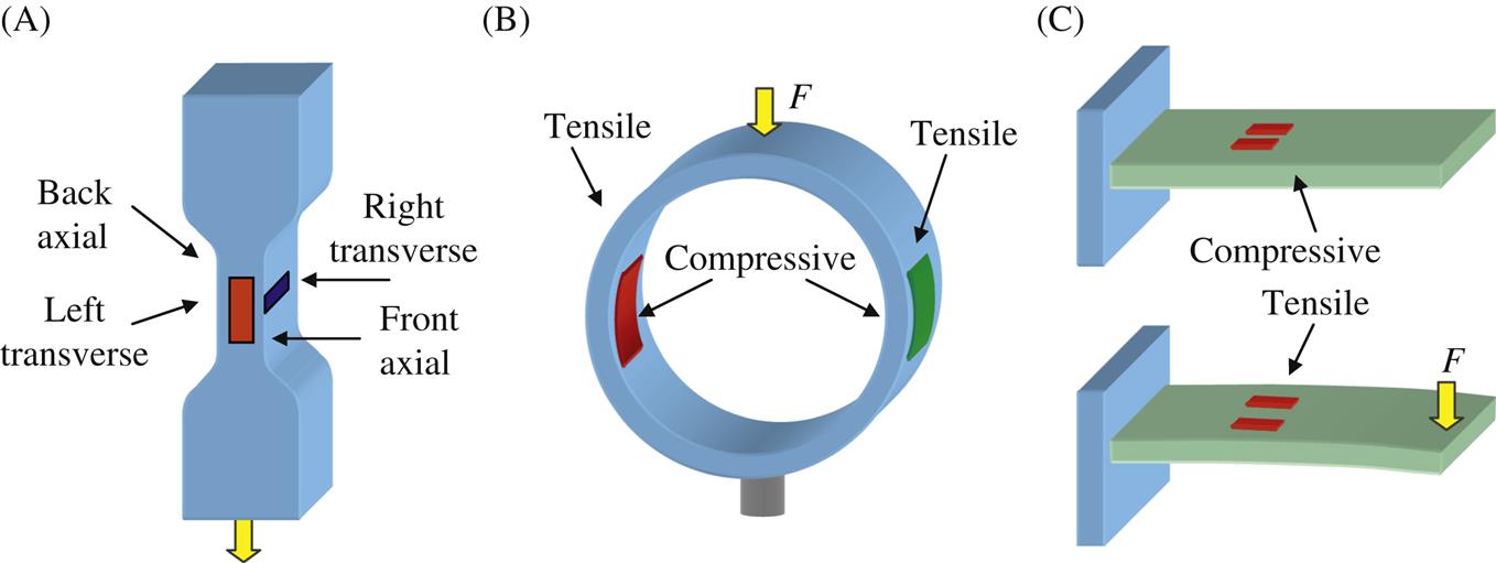
Fig. 4.15A presents a typical construction for large loads. The central part of the transducer is a metal bar with reduced cross-sectional area where gauges are mounted. There are four strain gauges in a full-bridge configuration. Two strain gauges (front and back side) measure the axial force, with equal sensitivity; two other gauges measure the transverse force, also with equal sensitivity. The gauges are arranged in the bridge of Fig. 3.3, according to the sequence (R1 front–R2 left–R3 back–R4 right). The axially positioned gauges respond to a strain as
and the resistance of the transverse gauges change as
Substitution in Eq. (4.23) and assuming ΔRi/Ri![]() 1 for all four gauges the bridge transfer is:
1 for all four gauges the bridge transfer is:
The applied force F is found using Hooke’s law or, rewritten in terms of force and deformation, F=(Δl/l)·AE, with A the cross-section area of the bar and E Young’s modulus of the material (or the elasticity c). Note that due to the Poisson ratio of the spring element, the compensating strain gauges (in the transverse direction) contribute significantly to the bridge output. With strain gauges mounted directly on a construction part the same relations between the bridge output and the force apply.
Fig. 4.15B shows a ring- or yoke-type spring element. Here the four strain gauges can be mounted in differential mode, compressive and tensile, with almost equal but opposite sensitivity to the applied force. For this arrangement Eq. (4.27) applies and full benefit from the advantages of a full bridge is achieved. The beam-type spring element of Fig. 4.15C allows a differential mode measurement of the strain as well. Although two strain gauges are sufficient (one on the top and one at the bottom), four gauges are preferred to build up a full bridge.
Torque measurements are performed in a similar way as axial force measurements. The strain gauges are positioned on the beam or shaft under angles of 45° relative to the main axis; see Fig. 4.16. Again four gauges are used to complete a full bridge: one pair experiences positive strain, the other negative strain. The transfer of a measurement bridge composed of these four gauges satisfies Eq. (4.27). Although the mutual position on the shaft is not critical, a close mounting is preferred to ensure equal temperatures of the gauges.
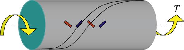
To determine the applied torque (or torsion moment) TM (Nm) from the response of the strain gauges, we use the relation between the torque and the shear stress Tshear (N/m2) at the outer surface of the shaft. For a circular, solid shaft, this is
with D the shaft diameter. Further, with Hooke’s law and assuming all normal stress components zero (pure torsion) the bridge output is found to be:
where K is the gauge factor of the strain gauges and ν the Poisson ratio of the shaft material.
When torque of a rotating shaft has to be measured, conventional wiring of the bridge circuit is not practical. Possible solutions are slip rings (wear sensitive) and transformer coupling (with coils around the rotating shaft). A contact-free torque measurement system is discussed in Chapter 7, Optical sensors.
Many motion control tasks require both torque and force information, up to all six degrees of freedom (d.o.f.). Special mechanical spring elements have been designed to simultaneously measure all these components. They are incorporated, for instance, between a link and the end effector of the machine. Such end-of-arm products are readily available from the market, in a variety of shapes, dimensions (down to 15 mm diameter), and measurement ranges.
A simple design of a force–torque sensor consists of a spring element with six or more strain gauges, mounted on a spring element of particular shape. A common spring type used for measuring all six components is the Maltese cross; see Fig. 4.17A for a simplified sketch. The wheel-like device is inserted in the robot element of which torque and force components have to be determined. Both element ends 1 and 2 are rigidly connected to the sensor 3: part 1 to the outer side and part 2 on the hub. On each of the four “spokes,” two pairs of strain gauges are mounted (Fig. 4.17B).

When a force or torque is applied to part 2 of the specimen, the eight differential pairs of strain gauges respond in proportion to these quantities, with a sensitivity that depends on the construction of the spring element. The gauges are arranged in a bridge configuration for obvious reasons. Each gauge pair responds to more than just one of the components Fx, Fy, Fz, Tx, Ty, and Tz. The sensitivity is described by the matrix equation:
where [F] is the 6×1 force–torque matrix, [S] the 1×8 strain matrix (if there are eight strain gauge pairs), and [C] is the 6×8 sensitivity matrix or coupling matrix of the spring element. The force and torque components are calculated using the inverse expression:
with [C]−1 the decoupling matrix. Note that [C]−1 strongly depends on the geometry of the spring element and on the position of the strain gauges.
Various other mechanical structures have been studied with the objective of combining minimal coupling between the force components with constructive simplicity. For instance, Ref. [9] gives an extensive analysis of a six-d.o.f. force–torque sensor for a robot gripper. The construction consists of a set of parallel-plate beams provided with strain gauges and allows the simultaneous measurement of three force and three torque components. The force and torque ranges of this combined sensor are 50 N and 5 Nm, respectively; interference (crosstalk) errors are around 1%.
Using finite element methods the sensitivity matrix can be calculated and the geometry can be optimized to a minimum coupling of the force–torque components (see, for instance, Refs [10,11]). However, tolerances in the positioning of the gauges and in the geometry of the spring element make calibration of the sensor necessary for accurate measurements of the force and torque vectors.
Sensor requirements for applications in the consumer market are much less strict compared to those in the precision manufacturing. In recent years, strain gauges have become the typical solution for measuring weight in various economically priced household equipment. A typical example is found in bathroom scales, where four yokes are mounted at the corners of the plate, each containing two strain gauges in half-bridge configuration (Fig. 4.18A). These four half-bridges are connected to form a full-bridge configuration, thereby summing the individual contributions to the total weight of the person standing on the plate. In kitchen scales, on the other hand, typically one yoke with a full-bridge configuration is used (Fig. 4.18B).

Integrated yokes measuring forces and torques along multiple axes are commonplace in robotic manipulators. The sensors are usually mounted just before the end effector. These sensor systems are highly integrated and have signal processing and acquisition hardware mounted in one single compact unit, shown in Fig. 4.19.

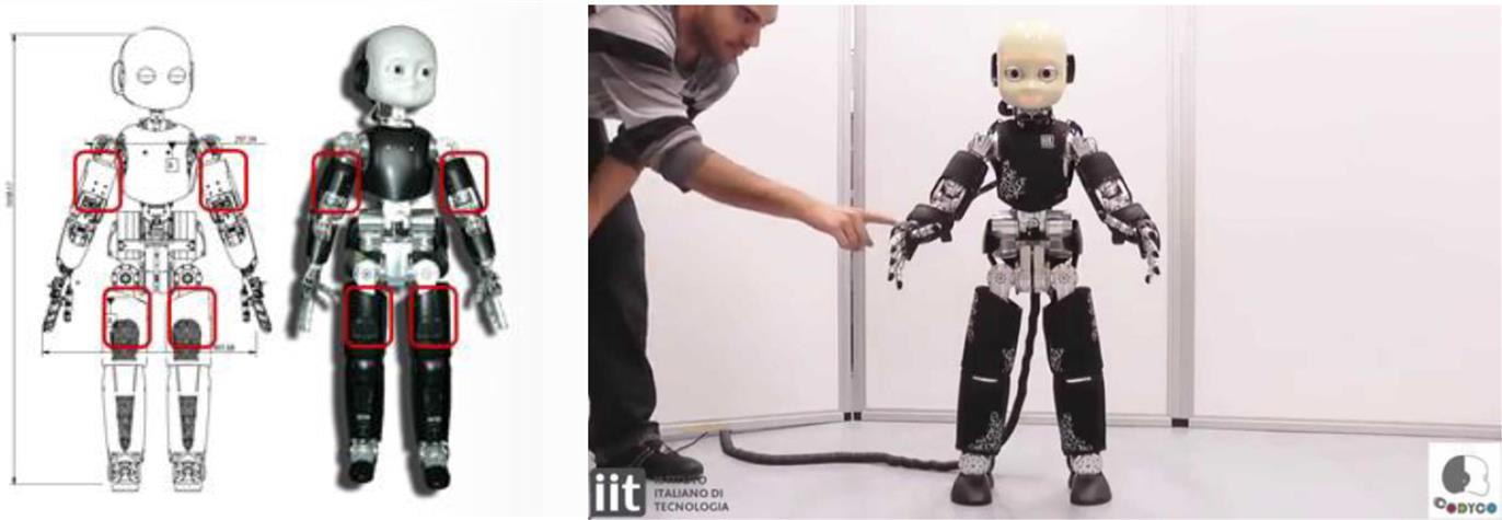
Also in humanoid robotics such as the iCub project (see Fig. 4.20), six-d.o.f. force/torque sensors are used to detect forces on the limbs, allowing advanced control strategies like gravity compensation, balancing and eventually walking.
4.4 Piezoresistive sensors
4.4.1 Piezoresistivity
Piezoresistive sensors are based on the change in electrical resistivity of a material when this is deformed. Many materials show piezoresistivity, but only those with a high sensitivity are suitable to be applied in sensors. Examples are semiconducting materials and some elastomers. The most popular piezoresistive semiconductor is silicon: this material can be used as the carrier of the sensor and, moreover, part of the interface electronics can be integrated with the sensor on the same carrier. Elastomers can be made piezoresistive by a special treatment, for instance by adding conductive particles to the nonconducting elastic material. This is discussed in Section 4.4.3.
The underlying physical principle of piezoresistivity in silicon goes back to the energy band structure of the silicon atom. An applied mechanical stress will change the band gap. Depending on the direction of the applied force with respect to the crystal orientation, the average mobility of electrons in n-type silicon is reduced, resulting in an increase of the resistivity. So the gauge factor of n-type silicon is negative and reaches values as high as −150. The absolute gauge factor increases with increasing doping concentration.
In p-silicon, holes are the majority carriers: their mobility is influenced by the position in the valance band. The gauge factor of p-silicon appears to be larger than n-silicon (at the same temperature and doping concentration), and has a positive value. In both cases the piezoresistive effect dominates the geometric effect (as used in metal strain gauges).
Table 4.4 shows numerical values for the gauge factor of p- and n-doped silicon, for three different crystal orientations, and a doping level corresponding to a resistivity of 1 Ωcm. Fig. 4.21 displays these three main crystal orientations of silicon.
Table 4.4
| Orientation | p-Type | n-Type |
|---|---|---|
| [111] | 173 | −13 |
| [110] | 121 | −89 |
| [100] | 5 | −153 |

Although the resistance change is primarily caused by material deformation, it is common use to express the piezoresistivity of silicon in terms of pressure sensitivity:
with K the gauge factor as defined in Eq. (4.12), π the piezoresistivity (m2/N) and S and T the mechanical strain and tension in the material, respectively. This is a simplified expression: the piezoresistive coefficient depends strongly on the direction of the applied force relative to the crystal orientation. The pressure sensitivity π of piezoresistive sensors (in silicon) depends on three factors:
The second factor in this list is related to the elastic behavior of the material as already described by the 6×6 compliance matrix (see Appendix A, Symbols and notations):
The combined orientation-dependent conductivity and compliance yields an expression for the relative resistance change r as a function of the vector T:
For silicon many of the matrix elements are zero due to crystal symmetry, and some are pair-wise equal. This results in the piezoresistivity matrix equation for silicon:
 (4.41)
So there are only three independent components describing the piezoresistivity of silicon. Their numerical values are given in Table 4.5.
Table 4.5
| Material | p-Type | n-Type |
|---|---|---|
| π11 | 66 | −1022 |
| π12 | −11 | 534 |
| π44 | 1381 | −136 |
n-Type silicon appears to have a strong negative piezoresistivity in the x-direction, and about half as much positive in the y- and z-directions; p-silicon is less sensitive in these directions. However, a shear force (with respect to an arbitrary direction) results in a large resistance change.
The unremitting progress in micromachining technology and the creation of microelectromechanical devices (MEMS) have great impact on sensor development. Advantages of this technology are
- • all piezoresistors are deposited in one processing step, resulting in almost identical properties;
- • the resistors on the membrane can be configured in a bridge;
- • the resistors have nearly the same temperature, due to the high thermal conductivity of silicon;
- • interface electronics, including further temperature compensation circuits, can be integrated with the sensor bridge on the same substrate;
- • the dimensions of the device can be extremely small; they are mainly set by the package size and the mechanical interface.
Sensors based on this technology are now widely spread, but much research is still going onto further improve the (overall) performance. MEMS also have their limitations, and other technologies are also being investigated and further developed to create better or cheaper sensors. There is also a tendency to combine technologies to benefit from the advantages provided by each of them.
4.4.2 Silicon piezoresistive sensors
Silicon technology allows the construction of a variety of sensors that make use of the piezoresistive properties of silicon. Examples are pressure and force sensors, accelerometers and gyroscopes.
Fig. 4.22 shows the basic configurations of a silicon pressure sensor and a silicon force sensor, both based on piezoresistive silicon.
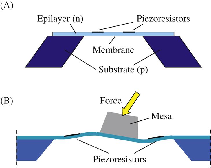
The sensor carrier or substrate is a silicon chip: a rectangular part cut from the wafer, with thickness about 0.6 mm. The wafer material is lightly doped with positive charge carriers, resulting in p-type silicon. On top of the wafer, a thin layer of n-type silicon is grown, called the epitaxial layer or epilayer. The substrate is locally etched away from the bottom up to the epitaxial layer, using selective etching technology. The result is a thin silicon membrane consisting of only the epitaxial layer, the thickness of which is some μm. This membrane acts as a deformable element.
Using standard silicon processing technology, piezoresistive sensors are deposited at positions on the membrane where the deformation is greatest. The gauge factor of silicon is much larger than that of metals; however, the temperature coefficient of the resistivity is also higher. Therefore silicon strain sensors are invariably configured in a full-bridge arrangement.
The silicon piezoresistors are deposited on the crystal surface, so they are technologically bound to a specific orientation (one of the orientations in Fig. 4.21). Once the surface orientation being chosen, the resistors have to be positioned such that maximum sensitivity is obtained. Piezoresistors usually have a meanderlike elongated shape, to obtain directional sensitivity in a restricted area (as with metal strain gauges). To optimize sensitivity the main axis of the resistor should coincide with the direction of maximal piezoresistivity on the membrane surface.
The membrane deforms under a pressure difference (as in Fig. 4.22A) or on an applied force (Fig. 4.22B). Special designs allow the measurement of both normal forces and shear forces. Independent measurement of the force components is accomplished by proper positioning of a set of piezoresistors on the membrane (see, for instance, Ref. [13]).
A common problem with all these types of sensors is the packaging. On the one hand the measurand (e.g., pressure and force) should have good access to the sensitive membrane in order to produce a deformation. On the other hand the silicon chip must be protected against mechanical damage. Gas pressure sensors are encapsulated in a small box provided with holes that give the gas access to the membrane, at the same time shielding the chip from direct mechanical contact with the outside world. Force sensors require mechanical contact between the membrane and the (solid) object, which is accomplished by a force-transmitting structure, for instance a small steel ball, a small piece of material fixed in the center of the membrane (a mesa) or a thin overlayer from an elastic material. In all cases this will affect the elastic properties of the membrane. In commercial force sensors the piezoresistors on the micromachined silicon are configured in a half- or full-bridge, to reduce temperature sensitivity.
The same technology is used to construct silicon accelerometers and gyroscopes. Fig. 4.23 shows the basic setup of an integrated accelerometer, consisting of a mass-and-spring element. All mechanical elements are created in silicon, by selective etching.
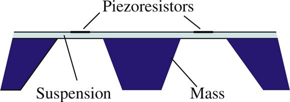
The seismic mass is an isolated part of the substrate, obtained by selective etching from the bottom side of the chip. The springs are silicon beams made from the epitaxial layer, by etching holes in the membrane. The mass suspends from the substrate by the thin beams, on top of which the piezoresistive elements are deposited. When the structure experiences an acceleration in a direction perpendicular to the chip surface, the mass will move up or down due to its inertia. The beams bend, and the piezoresistive elements respond to this deformation.
Since the device is sensitive to inertial forces, it can be packed in a hermetically closed housing, making it resistant against mechanical and chemical influences from the environment.
Silicon accelerometers with micromachined mass, spring, and integrated piezoresistors feature a high resonance frequency (up to 150 kHz), small dimensions and weight (down to 0.4 g) and low-cost. They are available with one, two, or three sensitive axes. Mounted at suitable spots on a mechatronic construction, they furnish useful information on position, orientation, and rotation of movable parts. The technology allows integration of the interface electronics with the sensor body, offering the prospect of very low-cost devices. One of the first silicon accelerometers with a complete interface circuit is described in Ref. [14]. The rectangular seismic mass is made using bulk micromachining and the circuit is realized in complementary metal-oxide semiconductor (CMOS) technology.
Micromachined gyroscopes are constructed likewise. They basically consist of a vibrating mass connected by a thin beam to the sensor base. The micromass vibrates in resonance mode (for instance by an electrostatic drive) and the corresponding bending of the beams is measured in two directions (preferably with four piezoresistors in full-bridge configuration as discussed in Chapter 3, Uncertainty aspects). Upon rotation of the structure the suspension undergoes torsion that is measured by piezoresistors integrated in the suspending beam. When the structure rotates, the vibration modes change, resulting in a phase shift of the bridge signals. Examples of such micromachined angular rate sensors with piezoresistive sensors are presented in Refs. [15,16].
4.4.3 Piezoresistive elastomers
Piezoresistive elastomers are elastomers that are made conductive by impregnation with conductive particles (e.g., carbon and silver). The resistivity depends on the concentration of conductive particles, their mutual distance and the contact area between touching particles.
When the material is pressed, more particles make contact, tending to decrease the resistivity of the material. The resistance between two adjacent or opposing points of the elastomer layer changes in a nonlinear way with the applied pressure. The blue squares (dark gray in print version) in Fig. 4.24 present a typical resistance–pressure characteristic, revealing that piezoresistive sensors are very sensitive (the resistance may change several orders of magnitude) but highly nonlinear [17]. The same figure shows that the conductance (i.e., 1/R) has an almost linear relation with the pressure (red diamonds (light gray in print version)). A suitable way of creating this reciprocal value is by using a standard inverting amplifier as discussed in Appendix C.4, Basic interface circuits.

Besides the nonlinear behavior, unfortunately most piezoresistive materials show also hysteresis, poor reproducibility, and creep, mainly because of permanent position changes of the conductive particles within the elastomer after being compressed, or lack of elasticity. The typical behavior of conductive elastomers is still not fully understood; many attempts are being made to model the piezoresistive properties in relation to composition and manufacturing methods (see, for instance, Ref. [18]). Despite poor performance of the sensing properties, some useful designs have been constructed and applied for a variety of applications where accuracy is not an important issue. Fig. 4.25 shows an example of such an elastomeric sensor, illustrating its small dimensions (thickness about 0.3–0.6 mm) and flexibility.

4.4.4 Applications of piezoresistive sensors
Piezoresistive sensors are suitable for the measurement of a variety of quantities. The word piezo is derived from the Greek piezein, which means to press, so pressure is an obvious quantity that can be measured by these sensors. However, many other physical quantities can be measured using the piezoresistive effect.
A 3D force sensor for biomedical applications is presented in Ref. [19]. The sensor has a construction similar to the one shown in Fig. 4.17 but is realized in silicon technology. Piezoresistors located at proper places on the square silicon frame (2.3×2.3 mm) measure three components of the force (0–2 N) applied to a short (one-half mm) protruding mesa. Evidently the sensor needs to be packaged in such a way that the externally applied force is properly transferred to the silicon mesa, at the same time providing an adequate mechanical and chemical protection.
Another application of a piezoresistive sensor is the displacement sensor described in Ref. [20], which is based on a conductive paste, deposited onto a piece of rubber. The high elasticity of the rubber and the paste allows large strain values, up to 40%. Its electrical resistance varies also roughly by this amount. As with all sensors based on piezoresistive elastomers, this sensor also exhibits a significant hysteresis. The sensor is designed for measuring the displacement of a soft actuator.
For the measurement of body parameters (e.g., posture, gesture, and gait), wearable sensors are being developed. Yarn-based sensors are a good solution for this application since they can easily be integrated into fabrics for clothing. Suitable sensor materials are piezoresistive polymers, rubbers, and carbon as coating material. Fibers from these materials can be interwoven with the textile. Stretching and bending of the textile result in elongation of the fibers, and hence a change in resistance. An application example of such wearable sensing is given in Ref. [21], reporting about such sensors for the measurement of aspiration. The elongation of the fiber can be as large as 23%, resulting in a resistance change of about 300%.
Piezoresistive sensors are also found in inclinometers. Such sensors measure the tilt angle, that is the angle with respect to the earth’s normal. Mounted on a robot, for instance, the sensor provides important data about its vertical orientation, which is of particular interest for walking (or legged) robots. In Ref. [22] a micromachined inclinometer was proposed, based on silicon piezoresistive sensors. The sensor consists of a micromass suspended on thin beams. Gravity forces the mass to move toward the earth’s center of gravity. The resulting bending of the beams is measured in two directions, by properly positioned integrated piezoresistors. The authors report an average sensitivity of about 0.1 mV per degree over a range of ±70° inclination.
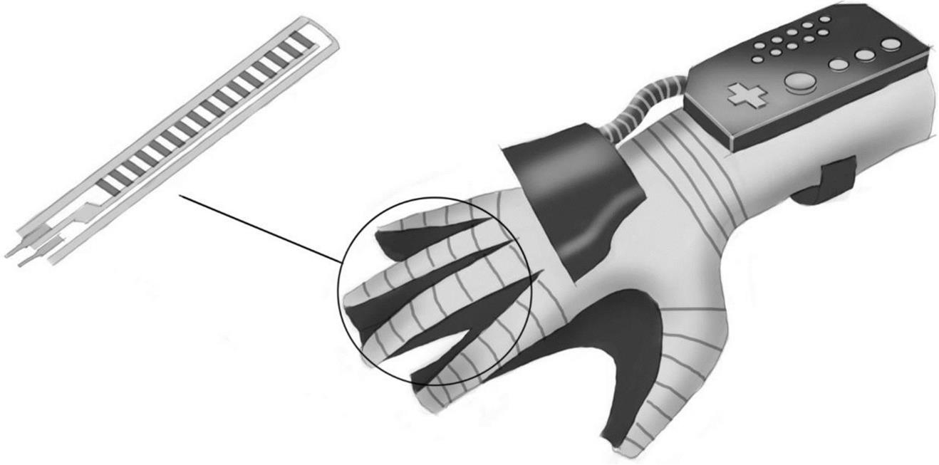
Resistive sensors based on piezoresistive elastomers can be manufactured as extremely flat devices, which offers a large amount of freedom for design and applications. Typically a sensor can be manufactured using a number of layers of durable plastic coated with the elastomer, combined with flexible tracks of a “normal” conductor. Besides measuring linear forces or shear forces these sensors can also be made into resistive bend sensors. Fig. 4.26 shows a typical resistive bend sensor using plastic foil and a resistive elastomer, applied in, for instance, a human–computer interface. These sensors are frequently applied in sensor gloves (such as the “grandfather” of sensor gloves: the Nintendo power glove shown in the same figure).
4.4.4.1 Tactile sensors
Piezoresistive elastomers can be used for a variety of sensing tasks in robotics. The pressure sensitivity of the bulk resistance is useful to sense touch (recall the high sensitivity for small forces), to measure gripping force and for tactile sensing. The material is shaped in sheets, which is very convenient for the construction of flat sensors, and in particular for tactile sensors.
Piezoresistive elastomers belong to the first tactile sensors in robot grippers [23,24]. They still receive much attention from designers of robots intended for human-like capabilities, in particular soft gripping (see, for example, Fig. 4.27).

Most resistive tactile sensors are based on some kind of piezoresistive elastomer and can be used for the construction of tactile sensors. Many researchers have reported on the usefulness of these so-called force-sensitive resistors as tactile sensors, for instance in Refs. [25–27].
Not only is the bulk resistivity a proper sensing parameter, but it is also possible to utilize the surface resistivity of such materials. The contact resistance between two conductive sheets or between one sheet and a conducting layer changes with pressure, mainly due to an increase of the contact area (Fig. 4.28). The resistance–pressure characteristic is similar to that of Fig. 4.24.

An important aspect of tactile sensors based on resistive sheets is the selection and readout of the individual pressure points (taxels). Most popular is the row–column readout, accomplished by a line grid of highly conductive electrodes on either side of the elastomer, making right angles and thus defining the pressure points of the sensor matrix (Fig. 4.29).
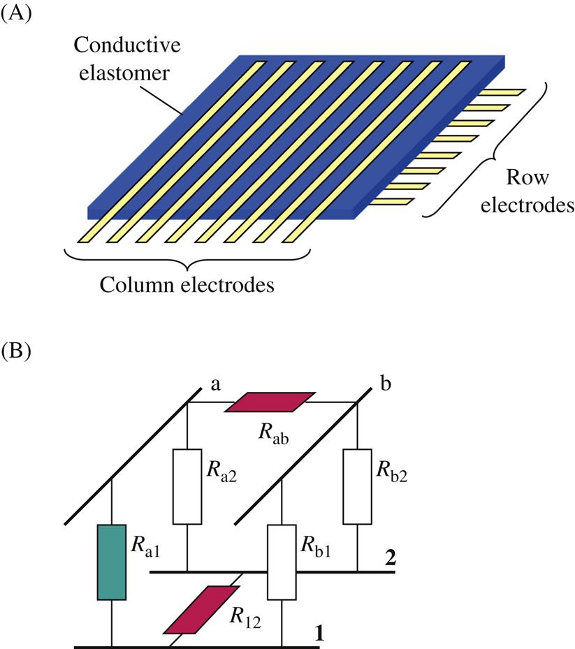
Individual taxels are addressed by selecting the corresponding row and column, for instance by applying a reference voltage on the column electrode and measuring the current through the selected row electrode. By using multiplexers for both the row and the column selection the whole matrix can be scanned quickly. However due to the continuous nature of the resistivity of the sheet, the selected taxel resistance is shunted by resistances of all other taxels, as can be seen in the model of the tactile sensor given in Fig. 4.28B. For instance when selecting taxel a−1, the taxel resistance Ra1 is shunted by resistances Rab+Rb1 and Ra2+R12, resulting in unwanted crosstalk between the taxels. Even when the interelectrode resistances Rab and R12 are large compared with the taxel resistances, the selected taxel resistance is shunted by Ra2+R2b+Rb1. As a consequence when one or more of the taxels a−2, b−2 and b−1 are loaded, the unloaded taxel a−1 is virtually loaded. This phenomenon is denoted by “phantom images.” In an n×m matrix many of such phantom images are seen by the selected taxel, an effect that is more pronounced when loading multiple taxels of the tactile device.
Crosstalk and phantom images are reduced by actively guarding the nonselected rows and columns, thus zeroing the potential over all nonselected taxels. The principle is illustrated with the simple 2×2 matrix of Fig. 4.30.

In Fig. 4.30A, selection of taxel a−1 is performed by connecting a voltage Va to column electrode a, and measuring the resulting current through row electrode 1, while all other rows and columns remain floating. Obviously since an additional current component I2 flows through the other three taxel resistances, the apparent taxel resistance amounts Va/I1=Ra1//(Ra2+R2b+Rb1). In Fig. 4.30B the nonselected row electrodes are all connected to ground; the additional current, which is now ![]() , flows directly to ground, so the measured resistance is Va/I1=Ra1, which is just the resistance of the selected taxel. Note that the current through the selected column electrode a can be quite large, in particular when many taxels on this column are loaded and thus have low resistance values to ground. Although not strictly necessary, grounding of the nonselected column electrodes is preferred too, to prevent possible interference due to the large resistance of nonloaded taxels. Various alternative schemes have been investigated aiming at increased effectiveness of this solution and reduction of electronic complexity, for instance in Refs. [28–30].
, flows directly to ground, so the measured resistance is Va/I1=Ra1, which is just the resistance of the selected taxel. Note that the current through the selected column electrode a can be quite large, in particular when many taxels on this column are loaded and thus have low resistance values to ground. Although not strictly necessary, grounding of the nonselected column electrodes is preferred too, to prevent possible interference due to the large resistance of nonloaded taxels. Various alternative schemes have been investigated aiming at increased effectiveness of this solution and reduction of electronic complexity, for instance in Refs. [28–30].
Many researchers have tried to increase the resolution of tactile sensors, at the same time reducing the major drawbacks as technical complexity, stiffness, dimensions, and susceptibility to damage. We give here a selection out of the many ideas published during the last few decades, as a source of inspiration for mechatronic designers.
Glued onto the elastic layer, the conductive electrodes affect significantly the elastic properties of the pressure sensitive material. Therefore the use of anisotropic elastomers has been proposed: this material shows a high conductivity in one direction and a low conductivity in perpendicular direction (see, for instance, Ref. [31]). Another solution is given in Ref. [30], where the functions of pressure sensitivity and readout electrodes are combined: the sensor consists of two orthogonally positioned arrays of conductive fibers. The 8×8 taxels are defined by the crossing points of the fibers. The contact resistance changes with pressure, mainly due to a reduction in contact area.
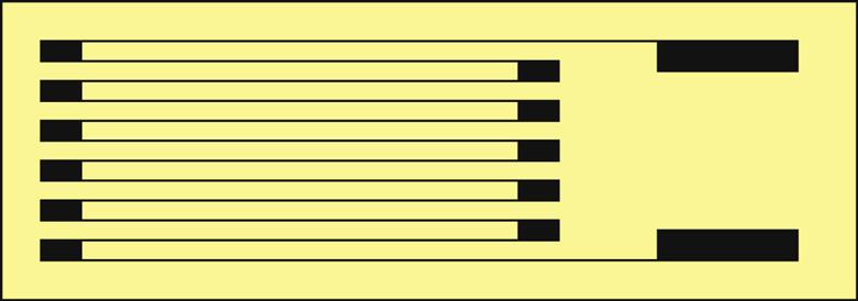
A completely different approach is to avoid having electrodes on top of the elastic layer, leaving the front side of the tactile sensor free to be accessed by objects. One of the solutions, applied in, for instance, the tactile sensor described in Ref. [32], is based on a double-sided printed circuit board. The 16×16 taxel sensor responds to the contact resistance between a highly conductive elastomeric sheet and an electrode pattern deposited on the printed circuit board. The layout of one taxel on the PCB is given in Fig. 4.31, showing how the crossings between column electrodes and row electrodes can be realized. The pressure sensitive part of each taxel consists of the two crossing areas between row and column.

An often overlooked aspect is mechanical crosstalk between adjacent taxels, due to the stiffness of the elastic layer or an additional protective layer. The sheet material acts as a spatial low-pass filter in the transduction from applied force at the top to the measurement side at the bottom of the sheet [33]. Hence the spatial resolution is not equal to the pitch of the electrodes but might be substantially lower.
Many attempts have been undertaken to increase the spatial resolution by applying silicon technology. One of the first results of this approach is described in Ref. [34], where the conductive elastomer is mounted on top of a silicon wafer, provided with electrodes and electronic circuitry to measure the (pressure sensitive) contact resistance. An all-silicon tactile sensor lacks the piezoresistive elastomer: it consists of an array or matrix of pressure sensors, similar to the devices shown in Section 4.4.2. A few examples of such completely integrated resistive tactile sensors are given here. The first one [35] consists of 32×32 piezoresistive bridges integrated on a single chip measuring 10×10 mm. The chip contains signal processing circuitry as well. To prevent damage when pressed the fragile sensor surface is covered with an elastic protective layer. A further example [36] concerns a 4×8 tactile sensor specifically designed for a large force range (up to 50 N). Finally in Ref. [37] a 4×4 tactile sensor with a different architecture is presented. The diaphragm layer is deposited over a matrix of small cavities at the top of the wafer, building up a matrix of membranes (without etching from the back side). Each element contains one piezoresistor. These resistors are connected sequentially to a Wheatstone bridge by controlling a set of on-chip CMOS switches.
Another aspect to be discussed here is the measurement of shear forces using a tactile sensor. Most of the devices discussed so far are only sensitive to normal forces, that is, a force pointing perpendicular to the sensor surface. A shear sensor should also be sensitive to tangential forces. Few resistive tactile sensors thus far offer this ability [38,39].
A frequently used alternative for resistive sensors as tactile sensors is the use of capacitive sensors. Also with capacitive sensors “taxels” can be created, for example the “skin” in the earlier mentioned robot “iCub” (Fig. 4.20) contains a large grid based on capacitive sensing. These systems will be described in Chapter 5, Capacitive sensors.
4.4.4.2 Touch sensors
Elastomer-based force sensors are not the most suitable for absolute (calibrated) force or weight measurement due to the nonlinear effects. Despite this fact the sensors have proven very suitable for other applications, illustrated by the design of a robotic foot of the robot Tulip [40] shown in Fig. 4.32. The sensors are very sensitive for “first touch” so good for detecting floor impact during walking. By measuring the difference between four sensors located at the corners of the foot the position of the center of mass can be determined accurately since unwanted effects (nonlinearity, temperature sensitivity, creep) affect all four sensors in the same way.

4.4.4.3 Touch screens
Resistive touch screens use a similar strategy as the tactile matrix described in Fig. 4.28. However, instead of an array of electrodes, only two electrodes are placed at opposite edges of a film coated with a uniformly distributed conductive coating. Two coated sheets are placed with the conductive layers facing each other, separated by a layer of spacer dots. Upon application of pressure (by a human finger or pointing device) two coupled voltage dividers are formed, allowing position detection, as shown in Fig. 4.33A. By biassing one of the dividers (i.e., the X-axis), one tap of the other axis can be used as sensing point as shown in Fig. 4.33B.

Although these resistive screens are still used in (industrial) human interface applications, they are largely replaced by capacitive screens because the latter have a higher repeatability and support multitouch. Resistive touch screens have to be recalibrated occasionally since the system relies on absolute resistive values, whereas a capacitive touch screen relies on sensing relative capacitive changes (Section 5.4.3).
4.4.5 Interfacing piezoresistive sensors
In this section a number of practical examples for interfacing piezoresistive sensors. Interfacing of these sensors for embedded applications will be discussed using the Arduino microcontroller platform introduced in Chapter 1, Introduction. Code examples and a more detailed discussion of the platform are given in Appendix D, Practical guideline and code examples.
In e-books on sensors (see, for instance, Ref. [41]), application examples dealing with qualitative analysis of sensor data can be found. In most cases a voltage divider circuit (Fig. 4.34A) is used to convert a resistive change into a voltage that can be measured using an ADC. However, a voltage divider introduces additional nonlinearities. When a sensor is placed in the lower branch of the divider (in other words: using a “pull up” resistor R1), the output voltage Vo satisfies Vi·Rsensor/(Rsensor+R1). Moreover, the pull-up (or pull-down) resistor might introduce additional (thermal) noise and temperature dependencies to the system. In Appendix C.2, Basic interface circuits, alternative circuits are discussed.

Fig. 4.34B illustrates a practical example of interfacing a nonlinear piezoresistive sensor using an inverting amplifier and negative voltage source. Using the graphwriter example code shown in Appendix D the circuit of Fig. 4.35 is a practical implementation of the circuit shown in Fig. 4.34B and can be used as linearization circuit.

When choosing the resistor values for pull-up or pull-down, the selection has to be in the expected range of the resistive sensor. Besides this match the sum of the resistances (sensor and pull-up/pull-down) should be high enough to minimize current consumption and reduce heating (I2R power dissipation). The ICL7660 is chosen in this case as supply voltage inverter. With the two capacitors this circuit generates a voltage of −5 V from the normal 5 V supply voltage. In the code now the measured voltage increases linearly with the applied force. For calibration a linear multiplication and offset might be sufficient.
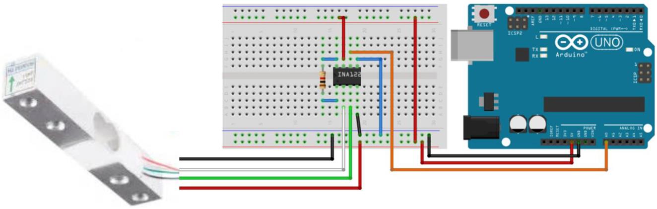
A load cell consisting of four strain gauges in bridge configuration as discussed in Section 3.2.1 can be interfaced using an instrumentation amplifier (Fig. 4.36). The voltage difference between the two branches of the Wheatstone bridge can be fed directly into the amplifier. In order to facilitate noise immunity an AC voltage could be applied to power the bridge (conf. Chapter 3, Uncertainty aspects), however, for the sake of simplicity the load cell will be powered by the supply voltage. Fig. 4.37 illustrates the interfacing of a load cell and the instrumentation amplifier to an Arduino board.

4.5 Magnetoresistive sensors
4.5.1 Magnetoresistivity
Some ferromagnetic alloys show anisotropic resistivity, which means that the resistivity depends on the direction of the current through the material. This property arises from the interaction between the charge carriers and the magnetic moments in the material. As a consequence the resistivity depends on the magnetization of the material. This effect, called anisotropic magnetoresistivity (AMR), was discovered by W. Thomson in 1856, and is manifest in materials as iron, nickel, and alloys of those metals (permalloy). The effect is rather small and requires very thin layers to be useful for sensing applications. In 1970 the first magnetoresistive head for magnetic recording appeared, but it was only in 1985 that a commercial tape drive with the magnetoresistive head was introduced in Ref. [42].
To describe anisotropic resistivity, Eq. (4.1) is rewritten into
Here ρx and ρy are the components of the resistivity in x- and y-directions. In general the resistivity is large in the direction of the magnetization and small in the perpendicular direction. Assume the magnetization is in the x-direction. If ϕ is the angle between the current density vector J and the magnetization vector M, the resistivity can be described by
or in a different way:
The material parameters ρ0 and β determine the sensitivity of the device. The angle ϕ runs from 0° (where the resistivity is maximal) to 90° (minimum resistivity). As an example, for a 50 nm thick layer of Permalloy, ρx is about 2×10⁻⁷ Ωm and ρy about 3×10⁻⁹ Ωm [43]. The sensitivity of an AMR material is usually expressed as
so the maximum relative change in resistivity (at room temperature) amounts a few % only. An external magnetic field in the y-direction will change the direction of the magnetization. So when the current remains flowing along the z-axis, the angle ϕ changes, and hence the resistivity of the layer (Fig. 4.38).

The magnetization vector M has a preferred direction, set by the shape of the ferromagnetic body. For a film-shaped body (length l, width w, and thickness t) the preferred magnetization is along the z-direction, with a strength that can be expressed by an effective magnetic field H0=(t/w)Ms. The relative change in resistance can now be expressed in terms of H0 and the external field Hy, according to the equations:
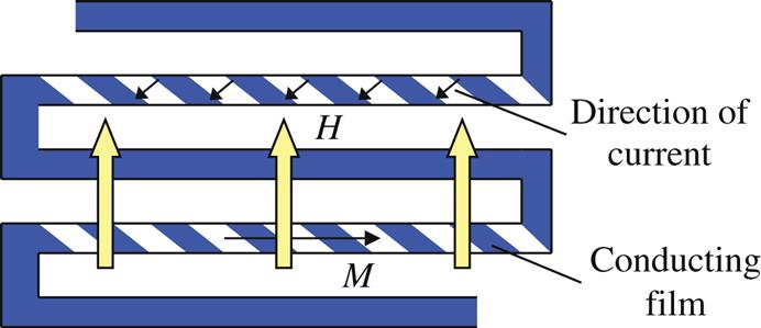
So the resistance decreases with the external magnetic field in both positive and negative y-direction. For sensor purposes, this symmetric sensitivity is very unlucky: it is strongly nonlinear and multivalued. To improve sensor behavior, an angle offset is required to shift the zero to, for instance, −45°. One way to achieve this is the introduction of an extra magnetic field. A more elegant way is to offset the direction of the measurement current I. This is accomplished by a special arrangement of the electrodes, called the “Barber pole” construction Ref. [44], after the similarity to the red-white spinning poles at barber shops (Fig. 4.39). Due to the low resistance of the electrodes (deposited as thin layers on the ferromagnetic sheet) the current is forced to flow through the device under an angle of approximately 45°. At zero field the angle between the current I and the magnetization M is 45°, corresponding to a resistivity of about half the minimum value. When a magnetic field is applied in positive y-direction, the angle decreases, so the resistivity increases and vice versa.
Commercial barber pole magnetic sensors contain four meanderlike structures as in Fig. 4.39, arranged in a full bridge to compensate for common mode errors. Typical data: measurement range 0–104 A/m (when specified in gauss, the range refers to magnetic induction B rather than magnetic field strength H and a conversion factor according to B=μ0μrH must be applied; see Chapter 6, Inductive and magnetic sensors, on inductive and magnetic sensors); temperature range −40°C up to 150°C, nonlinearity error 1% at FS sweep. Resolution and offset are mainly determined by the interface electronics; the resolution is good enough to measure the earth’s magnetic field, allowing compass heading (mobile robots) and attitude sensing (walking robots). Three-axis devices are available as well: they actually consist of three orthogonally positioned magnetosensors in one package.
Around 1980 magnetoresistive devices were realized that exhibit a much larger sensitivity, according to the so-called giant magnetic resistance (GMR) effect and the giant magnetic impedance (GMI) effect. A GMR device consists of a multilayer of ferromagnetic thin films (typically 1–10 nm thick), sandwiched between conductive but nonferromagnetic interlayers. The physical principle differs fundamentally from the AMR sensors. In the absence of an external field the magnetization in the successive layers of a GMR structure is antiparallel. In this state the resistance is maximum. At a sufficiently strong external magnetic field the magnetizations are in parallel, corresponding to a minimum resistance. The GMI sensor employs the skin effect, the phenomena in which conduction at high frequencies is restricted to a thin layer at the surface of the material. The axial impedance of an amorphous wire may change as much as 50% due to an applied magnetic field Ref. [45]. Present research is aiming at higher sensitivity, better thermal stability, and wider frequency range (see, for instance, Refs. [46,47]).
Commercial GMR sensors became available around 1995. Current research focuses on even higher sensitivity: in layered structures of amorphous ribbons made up of particular alloys, GMR ratios of up to 2400% have been reported [48]. Since GMR reading heads for magnetic discs are gradually replacing the older thin film AMR heads, there is some confusion about the terminology: GMR is now often called just MR or AMR.
In 1993 another group of materials, manganese-based perovskites, has been discovered exhibiting an even stronger magnetoresistive effect, at least at low temperatures and high magnetic fields. For this reason the effect is called colossal magnetoresistivity [49]. Unfortunately at room temperature the effect is much smaller, but nevertheless can be employed for sensor purposes [50].
Table 4.6 presents some specifications of these three types of magnetoresistive sensors. The resistors in the AMR sensor are configured as two Wheatstone bridges, allowing the measurement of the magnetic field in two orthogonal directions. The selected GMR sensor uses a Wheatstone bridge as well. Its output is a differential voltage, and a differential amplifier is required to convert this to a single-sided output. The GMI sensor in Table 4.6 consists of an amorphous metal wire with a pickup coil wrapped around the wire. This wire is driven by an AC current of 200 kHz. The frequency range of this sensor is, however, much lower compared to GMR and AMR: DC to 1 kHz. The sensor package contains three GMI sensing elements; the output signals are buffered in a sample-hold circuit, amplified and multiplexed.

4.5.2 Applications of magnetoresistive sensors
A magnetoresistive sensor measures essentially magnetic field strength. Therefore many applications are feasible, for instance as a compass (for mobile robots). Combined with a magnetic source (e.g., permanent magnet, active coil and earth magnetic field), magnetic field sensors are useful devices for the measurement of a variety of quantities in the mechanical domain.
Various possibilities for linear and angular position detection using AMR sensors are presented in Ref. [51]. In Ref. [52], AMR sensors are applied for vehicle detection: the sensors measure the change in earth magnetic field when a vehicle is passing the sensor. The system is used to monitor the traffic on highways.
GMR (and GMI) sensors too have been extensively tested for measuring a variety of mechanical quantities, for instance contact-free position [53], angle and speed [54], stress (in steel bars [55]), and torque [56]. They appear also useful for nondestructive testing [57] and, because of their small size, for biomedical applications; see, for instance, Refs. [58,59].
Most commercially available AMR sensors are manufactured as simple analog devices without additional processing “on chip” displayed graphically in Fig. 4.40. For further processing a separate ADC is necessary. This in contrary to, for example, Hall effect–based position sensors which are usually manufactured with a digital signal interface. In terms of performance, manufacturers list as advantages of AMR sensors compared with Hall effect sensors a higher sensitivity (so more cost effective since the necessary magnets can be smaller), smaller packages, and lower power consumption. Regarding applications in mechatronics, AMR sensors are used for similar purposes as Hall sensors (Section 6.2.2).
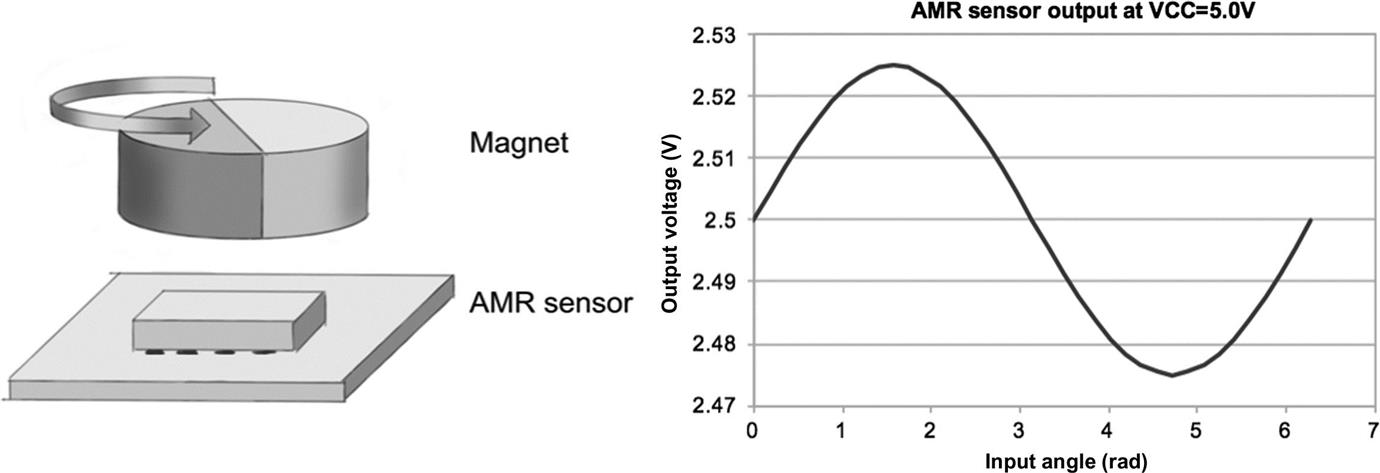
Properties of commercial magnetic sensors and applications based on the combination of a magnetic source and magnetic sensors will be discussed further in the chapter on inductive and magnetic sensors.
4.6 Thermoresistive sensors
4.6.1 Thermoresistivity
The resistivity of a conductive material depends on the concentration of free charge carriers and their mobility. The mobility is a parameter that accounts for the ability of charge carriers to move more or less freely throughout the atom lattice; their movement is constantly hampered by collisions. Both concentration and mobility vary with temperature, at a rate that depends strongly on the material.
In intrinsic (or pure) semiconductors the electrons are bound quite strongly to their atoms; only a very few have enough energy (at room temperature) to move freely. At increasing temperature, more electrons will gain sufficient energy to be freed from their atom, so the concentration of free-charge carriers increases with increasing temperature. As the temperature has much less effect on the mobility of the charge carriers, the resistivity of a semiconductor decreases with increasing temperature: its resistance has a negative temperature coefficient (NTC).
In metals all available charge carriers can move freely throughout the lattice, even at room temperature. Increasing the temperature will not affect the concentration. However at elevated temperatures, the lattice vibrations become stronger, increasing the possibility that the electrons will collide and hamper free movement throughout the material. Hence the resistivity of a metal increases at higher temperature: their resistivity has a positive temperature coefficient (PTC).
The temperature coefficient of the resistivity is used to construct temperature sensors. Both metals and semiconductors are applied. They are called (metal) resistance thermometers and thermistors, respectively.
4.6.2 Resistance thermometer
The construction of a high-quality resistance thermometer requires a material (metal) with a resistivity temperature coefficient that is stable and reproducible over a wide temperature range. By far the best material is platinum, due to a number of favorable properties. Platinum has a high melting point (1769°C), is chemically very stable, resistant against oxidation, and is available with high purity. Platinum resistance thermometers are used as international temperature standard for temperatures between the triple point of the hydrogen equilibrium (13.8033 K) and the freezing point of silver (+961.78°C) but can be used up to 1000°C.
A platinum thermometer has a high linearity. Its temperature characteristic is given by
with R(0) the resistance at 0°C. The values of the coefficients R(0), a, b, … are specified according to various standards and temperature ranges. As an example the resistance of a Pt100 is characterized, according to the DIN-IEC 751 standard, as
for a temperature range −200°C<T<0°C; for temperatures from 0 to 850°C the parameters a and b are the same, and c=0. The tolerances are also specified in the standard definition. For instance the resistance value of a “class A” Pt100 temperature sensor at 0°C is 0.06%, which corresponds to a temperature tolerance of 0.15K. At the upper end of the range (850°C) the tolerance is 0.14% or 1.85K. Class B sensors have wider specified tolerances, for instance 0.3K at 0°C.
There also exist resistance temperature sensors with other values than 100Ω at 0°C, for instance the Pt1000 with a resistance value of 1000Ω at 0°C. However, the Pt100 is most popular for industrial applications.
The sensitivity of a Pt100 is approximately 0.4%/K or 0.39Ω/K. The parameters b and c account for the nonlinear relationship between temperature and resistance. Within a limited temperature range the nonlinearity might be neglected, when a high accuracy is not required.
The tolerances and nonlinearity errors discussed so far relate to the sensor only. Additional errors may arise due to:
Self-heating should be minimized by reducing the current through the sensor and a low thermal resistance to the environment. A measurement current I introduces heat dissipation of I2R(T) in the sensor. For example at 0°C and 1 mA current the dissipation is 0.1 mW. In order to limit the error due to self-heating to 0.1°C the sensor should be mounted in such a way that the thermal resistance is less than 103 K/W.
Special integrated circuits are available that facilitate the interface between resistive sensors and a microprocessor or microcontroller. They are based on either single-, two-, or three-point calibration techniques (see Section 3.2.6). Present interface modules have high resolution and accuracy and are suitable for multisensor applications as well. For instance the interface circuit for a Pt1000 resistive temperature sensor presented in Ref. [60] has a resolution of 0.1Ω, a relative systematic error less than 0.01%, and a temperature coefficient of about 1.5×10⁻⁷/K over the range 10–50°C.
A simple analogue interface circuit for a resistance thermometer is shown in Fig. 4.41.
The output voltage of this circuit (assuming ideal properties of the operational amplifier and using the equations from Appendix C, Basic interface circuits) is
With the resistors R3 and R4 the output can be adjusted to zero at an arbitrary temperature (for instance 0°C). The resistor R1 sets the sensitivity of the circuit. Obviously the accuracy of this interface is set by the tolerances of the voltage source E and the resistances R1, R3, and R4, which all should be chosen in accordance to the required performance of the measurement system.
Resistive sensors can also be connected in a bridge configuration, in order to reduce nonlinearity and unwanted common mode interferences. The effect of cable resistance might be substantial, in particular when the sensor is located far from the measuring circuit. Its influence can be compensated (see Chapter 3, Uncertainty aspects).
4.6.3 Thermistors
A thermistor (contraction of the words thermally sensitive resistor) is a resistive temperature sensor built up from ceramics. Commonly used materials are sintered oxides from the iron group (e.g., chromium, manganese, nickel, cobalt, and iron); the most popular material is Mn3O4. These oxides are doped with elements of different valence to obtain a lower resistivity, giving them semiconductor properties (mainly of the p-type). Several other oxides are added to improve the reproducibility. To obtain a stable sensitivity, thermistors are aged by a special heat treatment. A typical value of the drift in resistance after aging treatment is +0.1% per year.
Thermistors cover a temperature range from −100 to +350°C, but particular types go down to 2 K (ruthenium oxide). Their sensitivity is much larger than that of metal resistance thermometers. Furthermore the size of thermistors can be very small, so that they are applicable for temperature measurements in or on small objects. Compared to metal resistance thermometers, a thermistor is less stable in time and shows a much larger nonlinearity.
The resistance of most semiconductors has a NTC. This also applies to thermistors. That is why a thermistor is also called an NTC-thermistor or just an NTC although also thermistors with a PTC do exist.
The temperature dependence of an NTC is given by
where R(T0) is the resistance at a reference temperature T0 (usually 25°C), B is a constant that depends on the type of NTC.
From this equation, it follows for the temperature coefficient (or sensitivity) of an NTC:
Further it should be realized that due to the nonlinearity of the temperature characteristic, the sensitivity varies with temperature (as also appears from the expression given above). The parameter B is in the order of 2000–5000 K. For instance at B=3600 K and room temperature (T=300 K) the sensitivity amounts to −4% per K. At 350 K the sensitivity has dropped to –3% per K.
The resistance value of a thermistor at the reference temperature depends on the material, the doping type and concentration, the device dimension and geometry. Values of R25 (the resistance at 25°C) range from a few ohms to some 100 kΩ. The accuracy of thermistors is in the order of ±1°C for standard types and ±0.2°C for high precision types.
Like metal resistive sensors, NTCs too suffer from self-heating. The current through the sensor should be kept low in order to avoid large errors due to self-heating. Generally a current less than 0.1 mA is acceptable in most cases (this is called zero-power mode). The effect of self-heating also depends on the encapsulation material and on the dimensions and shape of the sensor. In particular the condition of the environment (gas or liquid, still or flowing) determines the self-heating. A measure for this effect is the thermal dissipation constant, a figure that is provided by the manufacturer for various sensor types and various environmental conditions. It ranges from about 0.5 to some 10 mW/K.
The basic shape of a thermistor is a chip: a slice of ceramic material with metallized surfaces for the electrical contacts. The device is encapsulated in a coating of thermally conductive epoxy to ensure mechanical protection and a low thermal resistance to the measurement object. There are various shapes available: disc, glass bead, probe, surface mount. The smallest devices have a size down to 1 mm.
To measure the resistance value of an NTC the device can be connected in a single-element bridge (one NTC and three fixed resistances), or in a half- or full-bridge configuration (with two respectively four NTCs). This type of interfacing is used when small temperature changes or temperature differences have to be measured.
Thermistors are small-sized and low-cost temperature sensors, and useful in applications where accuracy is not a critical design parameter. They can be found in all kind of systems, for the purpose of temperature monitoring and control, for temperature compensation in electrical circuits (e.g., amplifiers and oscillators) and many other uses.
Besides NTC thermistors, there are also PTC thermistors. The base material is barium or strontium titanate, made semiconductive by adding particular impurities. The temperature effect differs essentially from that of a thermistor. PTCs have a PTC over a rather restricted temperature range. Altogether they cover a temperature range from 60 to 180°C. Within the range of a PTC the characteristic is approximated by
The sensitivity in that range is B (per K) and can be as high as 60% per K. PTCs are rarely used for temperature measurements, because of lack of reproducibility and the restricted temperature range of the individual device. They are mainly applied as safety components to prevent overheating at short circuits or overload.
A relatively recent and demanding application example for thermistors (NTC resistors) is the use in plastic extruder heads for 3D printers (Fig. 4.42). After many changes and design variations, currently almost every extruder design makes use of a similar 100 kΩ glass thermistor. This resistor typically has a temperature range between −50 and 260°C, and values for R(25) and B of 100 kΩ (±1%) and 3950 K, respectively.
4.7 Optoresistive sensors
The resistivity of some materials, for instance cadmium sulfide (CdS) and cadmium selenide (CdSe), depends on the intensity of incident light. This is called the photo-resistive effect. A resistor made up of such a material is the LDR (photoresistor). In the absence of light the concentration of free-charge carriers is low, hence the resistance of the LDR is high. When light falls on the material, free charge carriers are generated; the concentration increases and thus the resistance decreases with increasing intensity. The resistance of the LDR varies as
where Ed is the incident power per unit area, a and b being constants that depend on the material and the shape of the resistor.
The sensitivity of an LDR depends on the wavelength of the light, so it is expressed in terms of spectral sensitivity (ΔR/Ed per unit of wavelength). Fig. 4.43B shows the relative spectral sensitivity for two types of CdS resistors, one typical and one with high sensitivity for red light. The sensitivity is normalized to the maximum sensitivity within the bandwidth. Apparently below 400 nm and above 850 nm the LDR is not sensitive. The spectral sensitivity of this material matches rather well that of the human eye. Therefore the sensitivity is also expressed in terms of lux. For other wavelengths, other materials are used: in the near-IR region (1–3 μm) PbS and PbSe, and in the medium and far IR (up to 1000 μm), InSb, InAs, and many other alloys. Fig. 4.43A shows the resistance–illuminance characteristic of a typical CdS LDR. Note the strongly nonlinear response of the device.
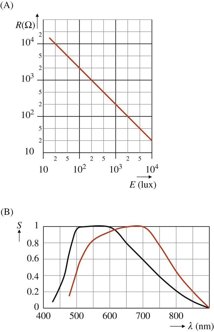
Even in complete darkness the resistance appears to be finite; this is the dark resistance of the LDR, which can be more than 10 MΩ. The light resistance is usually defined as the resistance at an intensity of 1000 lx; it may vary from 30 to 300 Ω for different types. Photoresistors change their resistance value rather slowly: the response time from dark to light is about 10 ms; from light to dark, the resistance varies only about 200 kΩ/s, resulting in a response time of about 1.5 s.
LDRs are used in situations where accuracy is not an important issue (dark–light detection only), for example in alarm systems, in the exposure-meter circuit of automatic cameras, and in detectors for switching streetlights on and off. Also in almost every starter kit for embedded control, an LDR is added as generic analog input device. The simplicity of use and convenient interfacing (using a voltage divider) make the LDR the standard device for getting started with (resistive) sensors in embedded systems.