
Piezoelectric sensors
Abstract
In this chapter we discuss principles, properties, and applications of piezoelectric sensors. A description of the piezoelectric effect is followed by an overview of the most common piezoelectric parameters. Piezoelectric materials are used in force sensors and accelerometers, the subject of the second section. Interface circuits for piezoelectric sensors are treated next, and various specific and original applications, including tactile sensors, are listed in the last section of this chapter.
Keywords
Piezoelectricity; constitutive equations; piezoelectric parameters; PZT; PVDF; piezoelectric accelerometer; interfacing; charge amplifier; applications
In this chapter we discuss principles, properties, and applications of piezoelectric sensors. A phenomenological description of the piezoelectric effect is followed by an overview of the most common piezoelectric parameters. Piezoelectric materials are used in force sensors and accelerometers, and for that reason they are found in many applications. Piezoelectricity can also be applied to construct acoustic transducers; this is the subject of Chapter 9.
8.1 Piezoelectricity
8.1.1 Piezoelectric materials
Piezoelectricity is encountered in some classes of crystalline materials. Deformation of such materials results in a change in electric polarization (the direct piezoelectric effect in Table 2.3): the positions of the positive and negative charges in the crystal are displaced relative to each other, causing a net polarization or change in intrinsic polarization. Fig. 8.1 shows a simplified 2D representation of this effect.
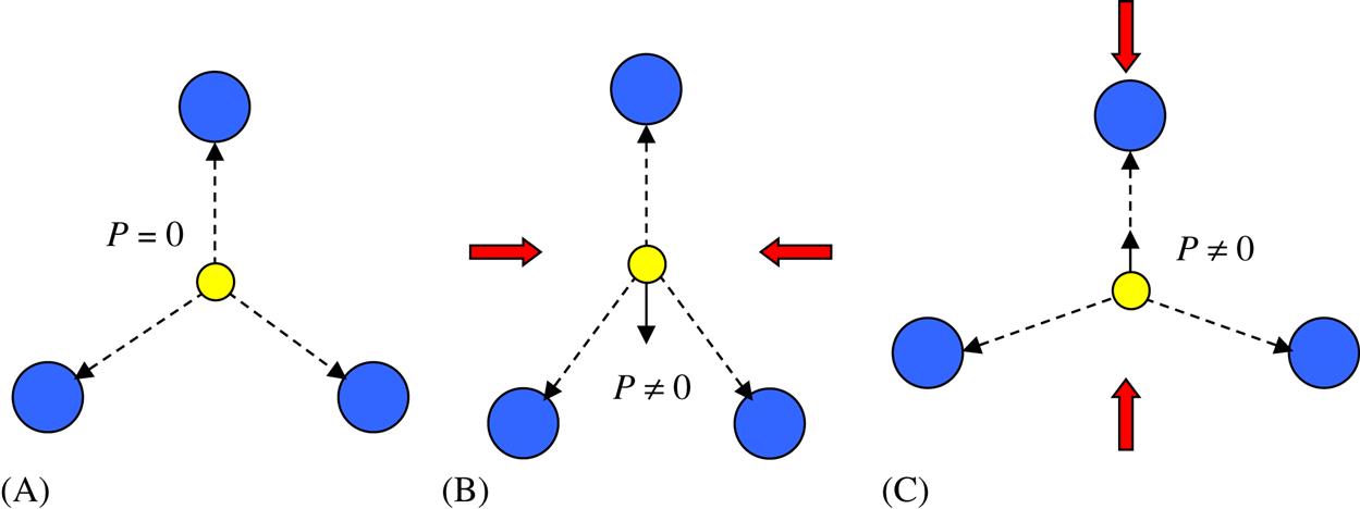
In Fig. 8.1A the structure is fully symmetric: the center of gravity of all positive charges coincides with that of the negative charges (the whole crystal is electrically neutral). When compressed in the horizontal direction (Fig. 8.1B), the center of positive charges has shifted downwards, resulting in a nonzero polarization. In case of a vertical compression (Fig. 8.1C), the center of positive charges has shifted upwards, resulting in a nonzero polarization in the other direction. This shift of positive charges relative to the negative charges produces opposite charges on the opposing surfaces of the crystal.
Evidently Fig. 8.1 is a strongly simplified representation of the piezoelectric phenomenon. Crystal structure, addition of dopants and other treatments of the material substantially determine the piezoelectric properties; for instance Ref. [1] shows the charge displacements for various compositions of PZT (lead–zirconium–titanate, a particular piezoelectric material).
The surface charge per unit area (C/m2) is proportional to the applied stress (N/m2), the charge (C) is proportional to the applied force (N). Generally the material is shaped as small rectangular blocks, cylinders, plates, or even sheets, with two parallel faces that are provided with a conducting layer. The construction behaves as a flat-plate capacitor, for which Q=C×V; so the output signal is available as a voltage. The sensitivity of such piezoelectric sensors is characterized either by the charge sensitivity Sq=Q/F (C/N) or by the voltage sensitivity Su=V/F=Sq/C (V/N). The piezoelectric effect is reversible (see Chapter 2): a voltage applied to the piezoelectric material results in a (small) deformation (the converse piezoelectric effect in Table 2.3); this property is used in piezoelectric actuators.
The following groups of materials exhibit piezoelectricity:
Natural piezoelectricity was discovered already in 1880 by the brothers Curie, in several crystalline materials [2]. The most known is quartz (crystalline silicon dioxide). It has a rather low but stable piezoelectricity, about 2 pC/N.
Materials of the second group contain electrical dipoles but are not piezoelectric, because the random orientation of the dipoles averages out, resulting in a zero net polarization. However, they can be made piezoelectric by poling: the material is heated up to the so-called Curie temperature, where the dipoles obtain high mobility. In this state a strong electric field is applied during a certain time period and the dipoles are oriented in the direction of the field. After slowly cooling down the dipoles maintain their orientation, giving the material its piezoelectric properties.
Compared to quartz, poled ceramic materials have a much higher piezoelectricity ranging from 100 up to over 1000 pC/N. The orientation of the dipoles slowly tends to a disordered state, resulting in a negative exponential decay in sensitivity over time:
(8.1)
where S(t) and S(t0) are the piezoelectric sensitivities at time t and the end of the polarization treatment time t0. The factor c in this expression lies in the range −5×10⁻² to −5×10⁻³ per decade at room temperature. For this reason the poled material is aged artificially, before being applied as a transducer. Mechanical and thermal shocks, however, may initiate new aging effects. Clearly the decay goes faster at higher temperatures. Note that even quartz loses its piezoelectricity above the Curie temperature, which is 573°C.
In 1969 Kawai discovered that some polymers can be made piezoelectric by poling under particular conditions [3,4]. The most popular piezoelectric polymer is polyvinylidene fluoride (PVDF, a chain of repeating units of CH2–CF2). The material is available in sheets with various thicknesses (6–100 μm) with conducting material deposited on its surface for connection purposes. PVDF has the highest piezoelectricity of all known polymers, about 25 pC/N. Poling is performed during stretching (in one or both directions), to obtain reasonable piezoelectricity. Piezoelectric PVDF has a limited temperature range, because its melting point is about 150°C, whereas the Curie temperature lies around 125°C. Since shortly after the material became commercially available the material has been successfully applied as a transducer in the thermal, mechanical, and acoustical domains [5,6].
An additional advantage of PVDF over ceramics is the compatibility with silicon technology. The thin sheets can be glued on top of a silicon wafer that contains part of the interface electronics. More recently piezoelectric copolymers of PVDF, for instance VDF/TrFE, have been developed. This material is available as a solution. It can be deposited on wafers by spinning [7]. Polymer-on-silicon technology opens up the possibility for the creation of smart (integrated) sensing devices, for the detection of pressure, force, sound, and thermal energy (the latter due to the fact that PVDF is pyroelectric as well) [8,9]. The major advantage of polymers over ceramic materials is their flexibility and small size (sheet thickness of several micrometers).
Another development concerns the deposition of thin film ceramics. This technology, too, can benefit from compatibility with integrated circuits and, using the reversibility of piezoelectricity, for microactuators [10].
The primary output quantity of a piezoelectric sensor is charge. In Section 8.3 we will show two basic schemes to convert that charge into a voltage: with a very high load impedance (open terminals) and with an almost zero load impedance (short-circuited terminals).
8.1.2 Piezoelectric parameters
In literature piezoelectric relations and properties are described in several ways. In this book we use the two-port description, which is analogous to the description of electrical two ports (Fig. 8.2). Two pairs of variables are involved: two input variables and two output variables. Each pair consists of one extensive and one intensive variable (see Section 2.2).

The relation between the four quantities can be described in various ways. For a linear electric network we can express the two voltages V1 and V2 as a linear function of the two currents I1 and I2:
(8.2)
or, in matrix notation:
(8.3)
In this description the matrix elements have a clear physical meaning: they represent electrical impedances. It is easy to find experimentally the input and output impedances of the system. For systems with no internal energy sources Z12=Z21. We assume this condition fulfilled in the remaining part of this chapter.
The input impedance is the ratio between input voltage and input current; likewise, the output impedance is the ratio between output voltage and output current. Note that the input impedance depends on the circuit connected to the output, and vice versa. We distinguish two cases: open- and short-circuited terminals. The input impedance of the system in Fig. 8.2 is:
(8.4)
(8.5)
For the output impedance we find:
(8.6)
(8.7)
Apparently input characteristics depend on what is connected at the output and vice versa. The degree of this mutual influence is expressed by the coupling factor κ, defined as:
(8.8)
The coupling factor is also related to the power transfer of the system. The maximum power transfer occurs for a load impedance equal to
(8.9)
Now we consider a piezoelectric sensor as a two-port network, analogous to the electrical system in Fig. 8.2, but this time with a mechanical input port and an electrical output port. In Chapter 2 we defined the relation between stress T and strain S:
(8.10)
Similarly the relation between dielectric displacement D and electrical field strength E is given by
(8.11)
where ε is the dielectric constant or permittivity (F/m). In piezoelectric materials mechanical and electrical quantities are coupled. A two-port model of a piezoelectric system is shown in Fig. 8.3.

The two-port equations of this system are, in general
(8.12)
and for linear systems in particular
(8.13)
that is, Eqs. (8.10) and (8.11) extended by the parameter g (m2/C or V m/N). Eq. (8.13) is the constitutive equation of the piezoelectric system. Mathematically sD is the partial derivative of S to T at constant D, and εT the partial derivative of D to E at constant mechanical tension T. From a physical point of view sD is the compliance at open electrical terminals (ΔD=0), and εT is the permittivity at open mechanical terminals (ΔT=0). The latter means that the material can freely deform: it is not clamped. At open electrical terminals the voltage generated by an applied force is E=−gT, which explains the name piezoelectric voltage constant for g.
Further as we have seen before the impedance of the connecting circuits (both mechanical and electrical) influence the properties of the material and hence the piezoelectric behavior. For instance the material’s stiffness is higher at short-circuited electrical terminals than when these terminals are open.
Another set of constitutive equation is:
(8.14)
which, for linear systems, becomes
(8.15)
where sE is the compliance at short-circuited electrical terminals (ΔE=0) and d (C/N or m/V) is the piezoelectric charge constant. At short-circuited terminals the electrical displacement, generated by an applied force, is found to be D=dT, which explains the name piezoelectric charge constant for the parameter d.
Other possible combinations of the electrical and mechanical quantities result in other material parameters, for instance εS: the permittivity at clamped state (ΔS=0). Further in literature the parameters e and h can be found. Table 8.1 shows an overview of all these piezoelectric parameters. The definitions are given as A/B|C, with A the quantity affected by B at constant C. We will use only d and g in the remaining of this chapter.
Table 8.1
| Parameter | Definition | Unit |
|---|---|---|
| d | D/T|E or S/E|T | C/N=m/V |
| e | D/S|E or T/E|S | C/m2=N/V m |
| g | E/T|D or S/D|T | V m/N=m2/C |
| h | E/S|D or T/D|S | V/m=N/C |
Relations between these four piezoelectric parameters follow from the respective constituent relations that define them (see for instance Refs. [11,12]). Irrespective of which set of constitutive equations is taken, they all describe the same material. Hence there is a relation between the various piezoelectric parameters. For instance the relation between d and g is:
(8.16)
Both g and d describe the strength of the piezoelectric effect of the material only; they do not depend on dimensions. The relations between sD and sE, respectively between εS and εT can be derived from the constitutive equations as follows:
(8.17)
(8.18)
where
(8.19)
is the piezoelectric coupling constant of the material (compare the coupling constant for an electrical two port in Eq. (8.8)). This coupling constant is an important parameter for the strength of the piezoelectric effect. Just as in the case of the electrical system the piezoelectric constant κ2 denotes the maximal fraction of (mechanical) energy stored in the crystal that can be converted into electrical energy (see for instance in Ref. [13]). Note that κ2 differs from the overall efficiency.
The equations given earlier only apply for isotropic materials, i.e., materials whose properties do not depend on the orientation within the material. Many piezoelectric materials are anisotropic. So similar to the parameters s and c the parameter ε should also be given as a matrix:
(8.20)
 (8.20)
Depending on symmetry in the crystal, some of the matrix elements are zero and others have equal numerical values. As an example Eq. (8.21) shows the permittivity matrices for quartz and ferroelectric Rochelle salt, respectively:
(8.21)
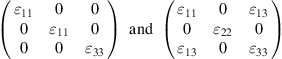 (8.21)
Hence the dielectric properties of quartz can be described by only two parameters: ε11 and ε33 (apparently ε11=ε22), whereas for Rochelle salt (NaKC4H4O6·H2O) four parameters suffice for the characterization of its piezoelectric properties.
Now the relationship between E and D is described with three linear equations:
(8.22)
 (8.22)
or in matrix notation:
(8.23)
where i, j are the directions x, y, and z in a given coordinate system. The parameters d and g, too, depend on the orientation of the mechanical parameters. Each of the six force components may result in a dielectric displacement in three directions. So for a piezoelectric material
(8.24)
or using the notation as presented in Chapter 2:
(8.25)
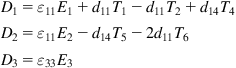
where i, j=1 … 3; k=1 … 6. Applied, for instance, to the displacement in x-direction (1-direction), this results in
(8.26)
Similar equations can be derived for D in the y- and z-directions, D2 and D3. In total the piezoelectric matrix contains 18 elements. Many of them are zero, due to the particular crystal structure. Moreover many of them are mutually dependent. As an example, for quartz, d12=−d11, d25=−d14, and d26=−2d11, due to the specific crystal structure of this material. So the 3×6 d-matrix in the equation Di=dik·Tk is [2, p. 18]:

with the numerical values d11=2.3×10⁻¹² C/N and d14=−0.7×10⁻¹² C/N. Hence the equations for D for quartz can be written as
(8.27)
 (8.27)
As an illustration we give here the piezoelectric d-matrices for two other piezoelectric materials: LiTaO3 (poled ceramic) and PVDF (poled after uniaxial stretching), respectively
(8.28)
 (8.28)
For a unique notation with respect to the orientation of polarized crystals, an agreement has been made saying that the z-axis (or 3-axis) is the direction of polarization. Fig. 8.4 visualizes various components of the d-matrix. In all these examples the electrical output (voltage or current) is measured in the direction of the polarization vector (3-direction), so the components of the matrix are all of the form d3i. In Fig. 8.4A the applied force is in the polarization direction. Many crystals have high piezoelectric sensitivity in this direction, which explains the often encountered parameter d33 in specification sheets. This mode of operation is called longitudinal, since the mechanical and electrical directions are the same.

In Fig. 8.4B a force is applied perpendicular to the direction of polarization: this is the transversal mode of operation. Transversal operation is used with crystals having a high value of d32. Fig. 8.4C shows a shear force in transversal direction (here the 4-direction), yielding the parameter d34. Finally in Fig. 8.4D the shear force is applied in the 6-direction, so the parameter d36 shows up.
Table 8.2 presents, for comparison purposes, various properties of a ceramic material based on PZT (lead–zirconium–titanate), of quartz and of PVDF. Note that the numerical values of all piezoelectric parameters depend on temperature, on composition, and on the manufacturing process. Detailed data are found in for instance Ref. [2]. Piezoelectric coefficients of PVDF and a measurement method for obtaining numerical values can be found in Ref. [14], for instance, where all piezoelectric constants according to Eq. (8.28) are presented.
Table 8.2
| Parameter | Symbol | PZTa | Quartz | PVDF |
|---|---|---|---|---|
| Density (kg/m3) | ρ | 7.6×10³ | 2.65×10³ | 1.78×10³ |
| Curie temperature (°C) | ΘC | 285 | 550 | 100–150 |
| Compliances (m2/N) | sE33 | 19×10−12 | 9.7×10⁻¹² | 4×10⁻¹⁰ |
| sE11 | 16×10−12 | 12.8×10⁻¹² | ||
| Permittivities | εT33/ε0 | 1700 | 4.6 | 10–13 |
| εT11/ε0 | 1730 | 4.5 | ||
| p.e. voltage constants (V m/N) | g33 | 27×10−3 | ||
| g31 | −11×10−3 | |||
| g11 | 0.06 | |||
| g14 | 0.02 | |||
| g15 | 33×10−3 | |||
| p.e. charge constants (C/N) | d33 | 425×10−12 | −18×10−12 | |
| d31 | −170×10−12 | |||
| d11 | 2.3×10⁻¹² | |||
| d14 | 0.7×10⁻¹² | |||
| d15 | 515×10−12 |
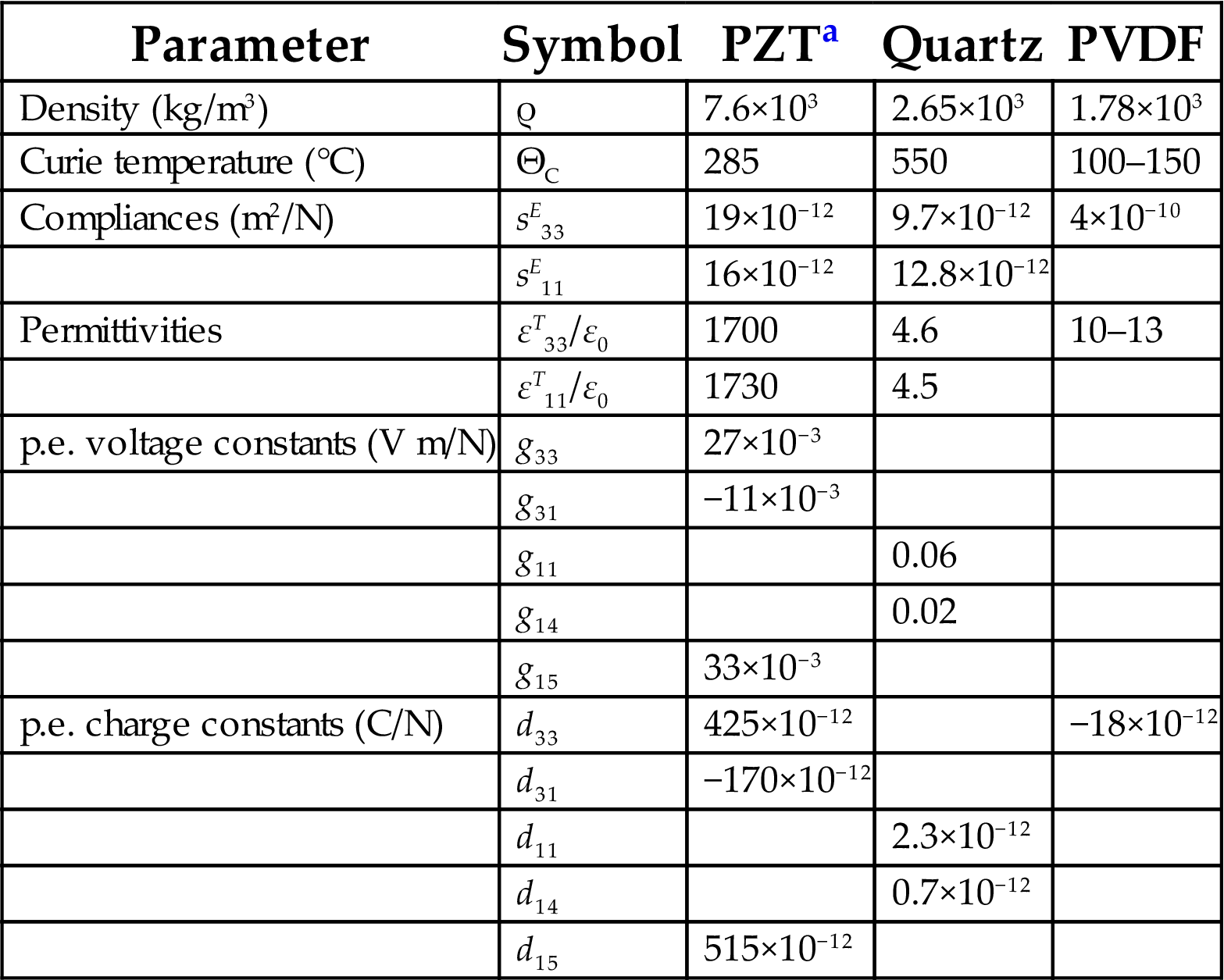
From data sheets of various manufacturers.
aData for a modified form of lead–zirconate–titanate; small modifications have a large effect on most piezoelectric properties.
8.2 Force, pressure, and acceleration sensors
8.2.1 Construction
Most force sensors are based on an elastic or spring element: the force generates a deformation that is measured by some displacement sensor (as discussed in previous chapters). The elasticity of the spring element determines the sensitivity of such sensors. A high sensitivity requires a large deformation, which is achieved by a low stiffness of the spring element. Such a large displacement, however, could unintentionally affect the structure in which the force has to be measured. A piezoelectric force sensor, on the other hand, responds directly to an applied force: the associated deformation is in most cases negligibly small, assuring small loading errors in the force measurement. Although force is the primary quantity that is measured by a piezoelectric sensor, other quantities such as pressure, strain, and acceleration can easily be measured as well, using a proper construction.
Piezoelectric sensors have disadvantages, too. The surface charge produced by an applied force might be neutralized easily by charges from the environment (airborne charges), by current leakage (due to a non-zero conductivity of the dielectric) or just by the input resistance of the connected electronics (discussed further in Section 8.3). This makes the sensor behave as a high-pass filter for input signals, impeding pure static measurements.
A further point of attention is the temperature sensitivity. There are various causes for this temperature effect. First piezoelectric materials are pyroelectric, so they also respond to temperature changes. Secondly a temperature change may induce crystal deformation and hence an electrical output as well. Further when materials connected to the piezoelectric crystals have different thermal expansion coefficients (for instance clamping parts and electrodes), the crystal experiences unwanted forces. Fortunately as long as these changes are slow, they would not limit the applicability because of the previously discussed intrinsic high-pass character.
Usually the elements of the transducer are kept together by clamping rather than by gluing. A consequence is that the crystals become preloaded. Fig. 8.5 shows in a very schematic way some basic constructions.
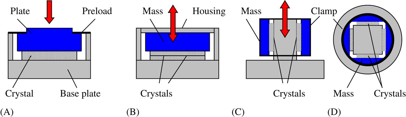
In a force sensor (Fig. 8.5A) the force to be measured is directly transferred to the piezoelectric crystal. Obviously the construction provides a means to connect the electrodes of the crystal to an external connector (not shown in the figure). Usually the case acts as the ground terminal.
In a piezoelectric pressure sensor the pressure to be measured is applied to a thin metal membrane. The total force on the membrane – that is the pressure times the active area of the membrane – is mechanically transferred to the crystal. Piezoelectric pressure sensors are also sensitive to acceleration, because the mass of the housing produces an inertial force on the crystal when accelerated. For applications where pressure has to be measured in a vibrating or otherwise moving environment, special pressure sensors are designed with a compensating crystal, to minimize the acceleration sensitivity.
An accelerometer consists basically of one or more piezoelectric crystals and a proof mass (or seismic mass). Here, also, the mass is fixed by a preload onto the crystal. Fig. 8.5B shows a compression mode accelerometer. This example comprises two crystals, mounted back to back between the seismic mass and the base plate. One electrode is connected to the common surface of the crystals, the other to the housing. In this configuration the crystals are electrically in parallel and mechanically in series, resulting in a doubled sensitivity. Moreover some compensation for common interferences is achieved. The shear-type accelerometer shown in Fig. 8.5C and D contains four crystals mounted on a rectangular post. The masses and crystals are fixed between a centre post and a clamping ring (as preload).
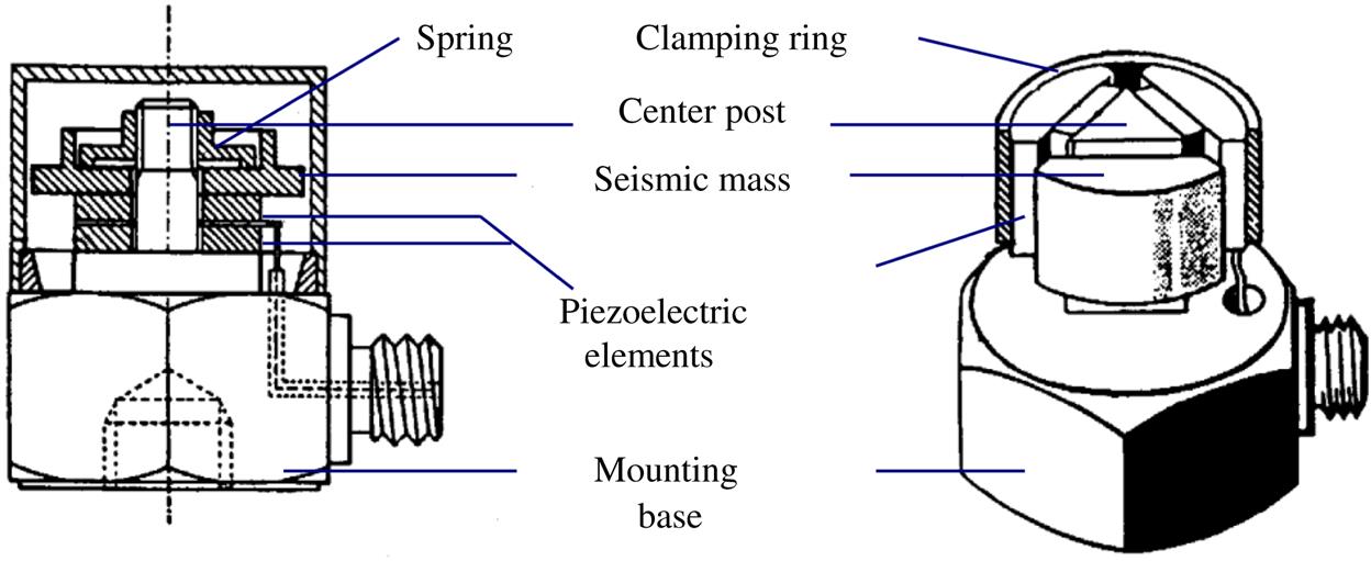
The absence of moving parts allows a piezoelectric sensor to be mounted in a robust package and hermetically sealed. Fig. 8.6 gives an impression of the real construction of the two accelerometer types shown in Fig. 8.5.
In both cases the main axis is in the vertical direction, where the sensitivity has a maximum value. Ideally the sensitivity in the orthogonal direction is zero. Commercial sensors have a non-zero sensitivity in directions perpendicular to the main axis, due to construction tolerances (not well-aligned crystals) or the cross sensitivity of the crystal itself. The crystal type and orientation should be chosen such that the highest value of d is in line with the main axis and zero for all other directions. For instance when d15 in the shear type is responsible for maximum output (in the 1-direction), the values of d12 and d13 should be zero, since these forces normal to the crystal may not generate an electrical output in that direction. Commercial accelerometers have a cross sensitivity that is just a few percent of the main sensitivity.
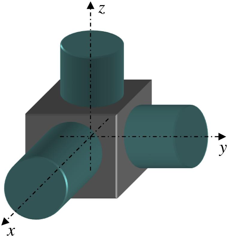
When two or all three components of a force or acceleration vector have to be measured, multi-axis sensors should be applied. The earlier three-axes versions usually consist of three separate sensors, mounted orthogonally in a single housing, as shown schematically in Fig. 8.7. The smallest dimensions of such sensors are comparable with a die and have a weight down to 20 g, and sensitivities of around 10 mV/g, where g is the gravitational acceleration in m/s2. More recently MEMS tri-axial accelerometers have flooded the market, mainly for consumer products (e.g. cameras and games). They are also available with integrated interface circuits. Typical sensitivities are 10–100 mV/g, and are 10–50 g in weight.
8.2.2 Characteristics of accelerometers
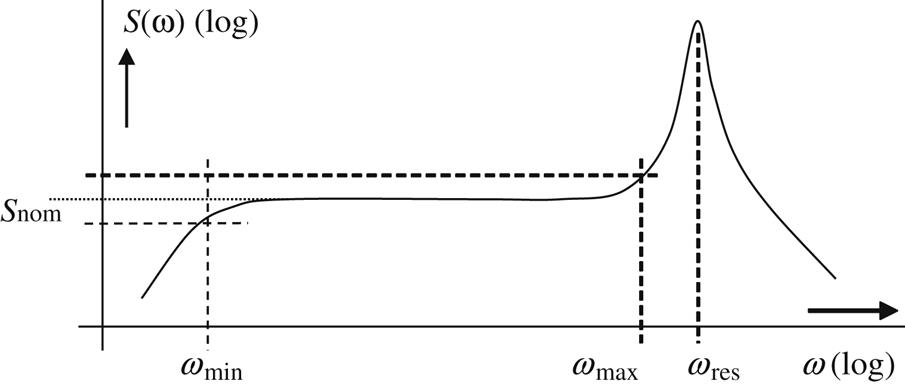
The frequency band of a piezoelectric accelerometer is limited at the lower side of the spectrum by the shunt resistance of the crystal (Section 8.2.1). At the upper side of the spectrum it is limited by the resonance frequency. Fig. 8.8 shows the useful frequency range of a standard type piezoelectric accelerometer. Here S(ω) is the sensitivity, that is the ratio between applied acceleration and electrical output, and Snom is the nominal sensitivity.
A piezoelectric accelerometer consists of a base plate, a seismic mass and a (preloaded) crystal. The mechanical characteristics of this spring-mass system follow from the equation of motion:
(8.29)
where m is the seismic mass, α the damping constant and k the spring constant (between seismic mass and base). The natural frequency of the system (i.e. the resonance frequency for α=0) equals:
(8.30)
The damping constant of a piezoelectric accelerometer is usually very small; in that case the (damped) resonance frequency ωres in Fig. 8.8 is close to ωo. A high resonance frequency requires a small mass m and a large stiffness k. The mass determines the sensitivity in the nominal frequency range and is chosen in accordance to the application. The resonance frequency of commercial accelerometers ranges from 1 to 250 kHz: the smaller the size, the higher the resonance frequency.
Many different types of piezoelectric sensors exist, for various applications. The smallest commercial accelerometers have a weight of 0.2 g and a resonance frequency at 50 kHz.
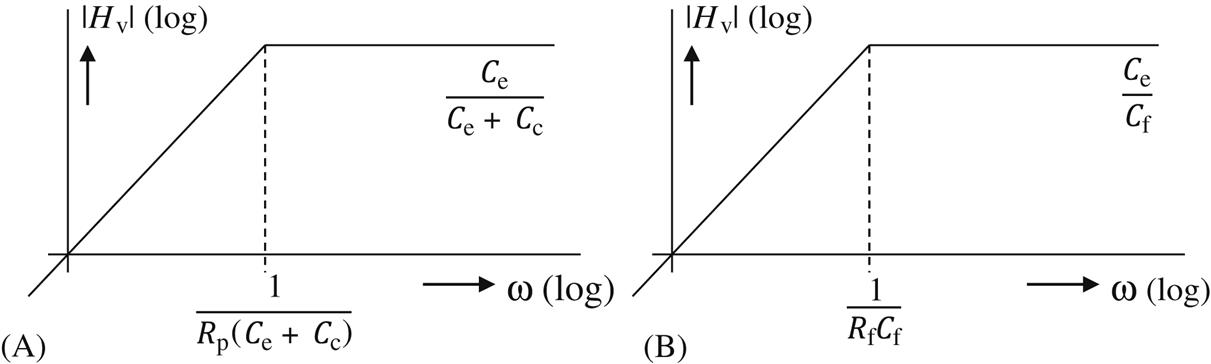
Table 8.3 lists the major properties of several groups of accelerometers and Table 8.4 shows some maximum ratings.
Table 8.3
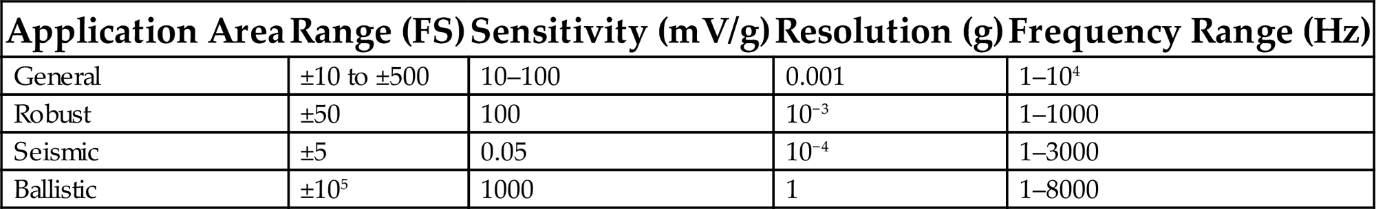
Table 8.4
| Type | Range (FS) | Sensitivity | Tmax (°C) |
|---|---|---|---|
| Acceleration | 103–106 m/s2 | 0.1–50 pC/ms−2 | 500 |
| Force | 102–106 N | 2–4 pC/N | 300 |
| Pressure | 107–108 Pa | 20–800 pC/MPa | 200 |

When applying piezoelectric sensors the following points should be considered:
- • Material properties depend on the electric load (open or closed electrical terminals); hence all sensor properties (sensitivity S, resonance frequency ωa) depend on the load too.
- • When mounting a sensor on an object, the latter is loaded mechanically, resulting in a change of acceleration a and resonance frequency ωa.
When M is the mass of the object and m the mass of the accelerometer, the acceleration is lowered by a factor 1+m/M, and the resonance frequency by a factor √(1+m/M), according to Eq. (8.30):
(8.31)
 (8.31)
where subscripts o and L denote the unloaded and loaded situation, respectively. These equations allow quick assessment of the loading effects when applying an accelerometer.
8.3 Interfacing
The primary signal of a piezoelectric sensor is charge Q. The sensor impedance behaves as a capacitance Ce, corresponding to the electrical capacity of a flat-plate capacitor with (piezoelectric) dielectric. This simple impedance model can be extended by a resistance Rs, modelling leakage currents (Fig. 8.9).
The charge signal can be measured in two different ways. The first method is based on the relation between charge and voltage over a capacitor: Q=C·V. Hence the interface circuit consists of a voltage amplifier. In the second method the charge is allowed to flow through an impedance, preferably a capacitor. The voltage across this capacitor is proportional to the charge. This type of interface is commonly called a charge amplifier; a better name would be charge–voltage converter.
Fig. 8.10 shows examples of these interface circuits, together with models for the sensor and the connecting cable (the part between the dotted lines). It will be shown that the cable capacitance can have a substantial influence on the signal transfer of the system, due to the capacitive character of the sensor. The sensor is modelled by the voltage source model of Fig. 8.9B.

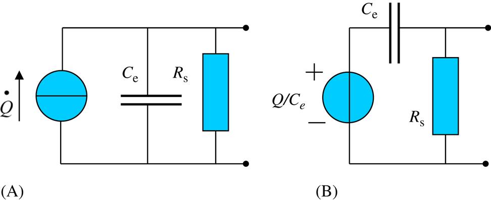
We calculate, for both interface circuits, the total signal transfer, using the formula for operational amplifier configurations in Appendix C. First we consider the voltage readout (Fig. 8.10A). The transfer of this circuit is given by
(8.32)
where Rp=Rs//Rc (parallel connection) and A=1+R2/R1, the gain of the non-inverting amplifier. Obviously the transfer shows a high-pass character (Fig. 8.11A): for frequencies satisfying ωRp(Ce+Cc)![]() 1 the transfer equals Ce/(Ce+Cc), so it is frequency independent. The cable capacitance Cc causes signal attenuation. Hence the total signal transfer depends on the length of the cable. This requires recalibration each time the connection cable is replaced.
1 the transfer equals Ce/(Ce+Cc), so it is frequency independent. The cable capacitance Cc causes signal attenuation. Hence the total signal transfer depends on the length of the cable. This requires recalibration each time the connection cable is replaced.
The interface circuit of Fig. 8.10B is better, in this respect. Due to the virtual ground of the operational amplifier the voltage across the sensor and the cable is kept at zero: neither the cable impedance nor the input impedance of the amplifier influences the transfer, and hence can be ignored. Assuming an ideal operational amplifier, its output voltage is −Z2/Z1. Without resistor Rf, Z1=1/jωCe and Z2=1/jωCf, hence the output voltage equals Vo=− (Ce/Cf)(Q/Ce) which, indeed, does not depend on cable properties.
Ideally the circuit with a capacitor in the feedback path behaves as an integrator: the input current flows through Cf resulting in a voltage equal to (1/Cf)∫Idt. Here the input current is generated by the piezoelectric sensor and equals dQ/dt, that is the time derivative of the piezoelectrically induced charge Q. Hence the voltage across Cf is just Q/Cf explaining the name charge amplifier.
Unfortunately the integrator does not only integrate the input charge, but also the unavoidable offset voltage and bias current of the operational amplifier. To prevent the amplifier from overloading, the feedback resistor Rf cannot be left out. This results in a transfer given by
(8.33)
Just as in Eq. (8.32), this transfer has a high-pass characteristic (Fig. 8.11B): the cut-off frequency is set by the components of the amplifier only: for ωRfCf![]() 1 the voltage transfer is −(Ce/Cf). When using a high quality operational amplifier (low offset, low bias current), the value of the cut-off frequency can be chosen down to 0.01 Hz. A true static measurement of acceleration or force, however, is not possible.
1 the voltage transfer is −(Ce/Cf). When using a high quality operational amplifier (low offset, low bias current), the value of the cut-off frequency can be chosen down to 0.01 Hz. A true static measurement of acceleration or force, however, is not possible.
8.4 Applications
Piezoelectric force sensors and accelerometers are available for a wide range of applications. They can be mounted on proper places of the mechatronic construction, taking into account mechanical loading and direction of sensitivity. If only little space is available for mounting a commercial device, single piezoelectric crystals could be used, taking note of the polarization direction, the orientation of the electrical contact surfaces and a proper interfacing. Charge amplifiers are preferred in most cases.
In this section we present some examples of special designs of piezoelectric sensors for various applications.
8.4.1 Stress and pressure
Axially stressed and poled PVDF shows a rather strong piezoelectric effect (Table 8.2). A straightforward design of a pressure sensor using this property is a sheet of PVDF on top of a rigid backing, making use of lateral deformation. However the flexibility of PVDF allows the material to bend easily, so it can serve as a membrane, resulting in a much higher pressure sensitivity. Two pressure sensors designed according to this concept are presented in Ref. [15]. A circularly shaped sheet of piezoelectric PVDF 5 mm in diameter and about 25 μm thickness, with metallization layers on both sides, is clamped between two parts of a likewise circular housing made up of PVDF. The sensor is applied in pneumatic and hydraulic systems, for pressures up to 200 kPa and temperatures up to 125°C and is resistant to a wide range of chemicals. Many properties of the prototype have been determined experimentally: sensitivity to temperature and humidity, response time (less than 100 μs), frequency range and stability over time (i.e. aging and creep). As outlined in preceding sections, the sensor element is also pyroelectric, so it responds to temperature changes as well, and shows a high-pass characteristic that depends on the temperature-dependent loss factor (resistance) of the membrane.
Ice deposition, for instance on overhead power transmission lines and power pylons, may cause much damage, and it is useful to study the adhesion at different conditions. In Ref. [16] PVDF is used to measure interfacial stress between an ice layer deposited on an aluminium substrate. Clearly the small thickness of PVDF as well as its flexibility makes this sensing material an excellent candidate for this task. It is shown that an embedded PVDF layer provides useful information about ice de-bonding stress and propagation.
Many examples can be found in literature illustrating the versatility of PVDF as a means to measure pressure and obtain pressure images. For instance Ref. [17] describes a system for measuring the dynamic (normal) pressure between a car’s tyre and the ground, and in Refs [18,19] the material is used for automatic verification of hand-written signatures.
8.4.2 Acceleration
Most piezoelectric accelerometers for industrial application are designed according to Fig. 8.5. The present market offers a vast variety of types for almost any application. However proposals for alternative designs aiming at even better performances or for particular applications appear on a regular basis in scientific literature. For instance the advent of piezoelectric PVDF and the fast development of microtechnology motivate researchers for looking to new solutions for both old and new measurement problems.
Soon after its discovery piezoelectric PVDF was recognized as being a suitable sensing material. Moreover the light-weight film-shaped material allows the construction of small and cheap accelerometers. An early attempt to create a PVDF-based accelerometer is found in Ref. [20], which shows a sensor for accelerations up to an acceleration of 50,000 g. An angular acceleration sensor can be created as well, as shown in Ref. [21]. By a special geometric arrangement of four piezoelectric elements (PVDF) and two seismic masses, an angular sensitivity of about 0.1 pC/rad/s2 has been achieved.
By suspending a seismic mass on a sheet of PVDF, a very sensitive accelerometer has been achieved, to be used for very low frequencies as a replacement for a geophone [22]. The resonance frequency (Fig. 8.8) amounts to 265 Hz for a particular choice of the parameters; the sensitivity is almost constant up to 100 Hz.
Another way to realize small, sensitive accelerometers is the use of thin films of PZT (typically 1–5 μm). In this case the piezoelectric material is one of a sandwich of thin layers deposited on a silicon substrate [23]. Other layers serve as electrodes and isolation. The seismic mass is formed by selective etching of the substrate, resulting in a mass-spring system similar to the one shown in Figure 4.18. The structure is sensitive in three directions, 22 pC/g for transversal and 8 pC/g for in-plane acceleration. An extensive FEM analysis of such thin-film piezoelectric accelerometers is given in Ref. [24], providing guidelines for the design of devices with specified properties.
A different approach is followed in Ref. [25], in which the PZT is deposited in a thick layer (typically 50 μm), on an alumina substrate. This device is composed of two sensing elements, to compensate for temperature effects. They also serve as seismic mass. The sensitivity can be set by an additional amplifier and is constant between 1 Hz and 10 kHz.
The reversibility of the piezoelectric effect provides solutions with a combination of actuation and sensing. In Ref. [26] such a combined piezoelectric sensor–actuator system is used to reduce vibrations that may occur in precision mechatronic systems, in this example a waver stepper. A piezoelectric ceramic sensor (1 mm thickness) measures vibrations in a particular part of the construction, and a stack of piezoelectric actuators (4 mm thickness) generates a counter-movement in the same part of the construction. With a proper design of the control loop, the amplitude of the dominant vibration mode is reduced by a factor of 7.
8.4.3 Tactile sensors
Piezoelectricity is one of the many physical effects that have been explored for the realization of tactile sensors. In particular the piezoelectric polymer PVDF has attracted much attention. The small dimensions in the direction of the force, as well as the flexibility of the material, simplify integration of PVDF tactile sensors in a robot gripper, even on the fingers of a dextrous gripper [27]. One drawback of the material is the charge leakage (preventing the measurement of static images). Moreover the material is also pyroelectric, which makes the sensor sensitive to temperature changes and gradients as well; hence this property could be put to use in robotics when thermal data about objects (i.e. temperature and thermal conductivity) add useful information to the control system, somewhat similar to the human skin [28–30].
Like other tactile sensors discussed in preceding chapters, piezoelectric tactile sensors too are used for two important tasks: contour recognition and improving gripper control [31,32]. In Ref. [32] a study on a thick (1 mm) piezoelectric tactile sensor is presented. The sensor is modelled as a second-order system and shows a frequency characteristic similar to the one given in Fig. 8.8, with a resonance frequency of 6.1 kHz. In applications where dynamic performance matters (for instance as an active rate of force sensor described in Ref. [33]), PVDF sensors appear to be suitable devices.
A common problem in tactile sensing for contour measurement is the low spatial resolution. Piezoelectric sensors suffer from this problem too, although sensors have been realized that are able to determine the orientation of objects on a test bed equipped with a piezoelectric polymer [30].
Piezoelectric ceramics and polymers are also applied in the acoustic domain. Application examples, including tactile sensors, will be discussed in the next chapter on acoustic sensors.
The integration of polymer technology and silicon technology offers interesting prospects for future developments of compact, high-resolution tactile sensors with integrated electronics.