
Basic interface circuits
In this appendix, we review the transfer functions of some basic electronic circuits, to facilitate the understanding of the interface circuits as used throughout the text. All circuits are built up with operational amplifiers. Circuits and associated transfer functions are given for the current-to-voltage converter, inverting and noninverting amplifiers, differential amplifier, integrator, differentiator and some analogue filter circuits. In the first instance, the operational amplifier is considered to have ideal characteristics. Where appropriate the consequences of a deviation from the ideal behavior are given, as well as measures to reduce such unwanted effects.
C.1 Operational amplifier
The symbol for an operational amplifier is given in Fig. C.1A. Usually the power supply connections are left out (which will be done hereafter). The model in Fig. C.1B shows the major deviations from the ideal behavior.
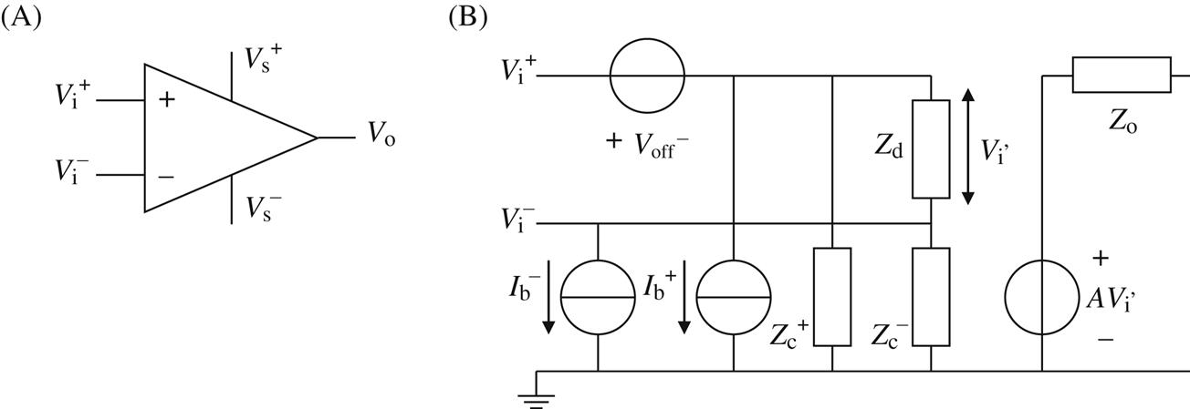
The meaning of these circuit elements is as follows:
- A: voltage gain (frequency dependent); A0: low-frequency voltage gain,
- Voff: input offset voltage,
- Ib+ and Ib−: input bias currents through the plus and minus terminals,
- Ioff=|Ib+−Ib−|: input offset current,
- Zc− and Zc+: common input impedances from either input to ground,
- Zd: differential input impedance (between the two input terminals), and
- Zo: output impedance.
Further, the common mode rejection ratio (CMRR) accounts for the suppression of pure common mode signals relative to differential mode signals. Finally, amplifier noise is specified in terms of (spectral) voltage noise and current noise. For white noise these error sources are specified in terms of V/√Hz and A/√Hz, respectively. In Fig. C.1, the noise voltage can be modeled with a voltage source in series with the offset voltage, and the noise current by a current source in parallel to the bias current. For an ideal operational amplifier A, Zc, Zd and H are infinite, and Voff, Ib and Zo are all zero. Any deviation of these ideal values is reflected in the transfer properties of interface circuits built up with operational amplifiers.
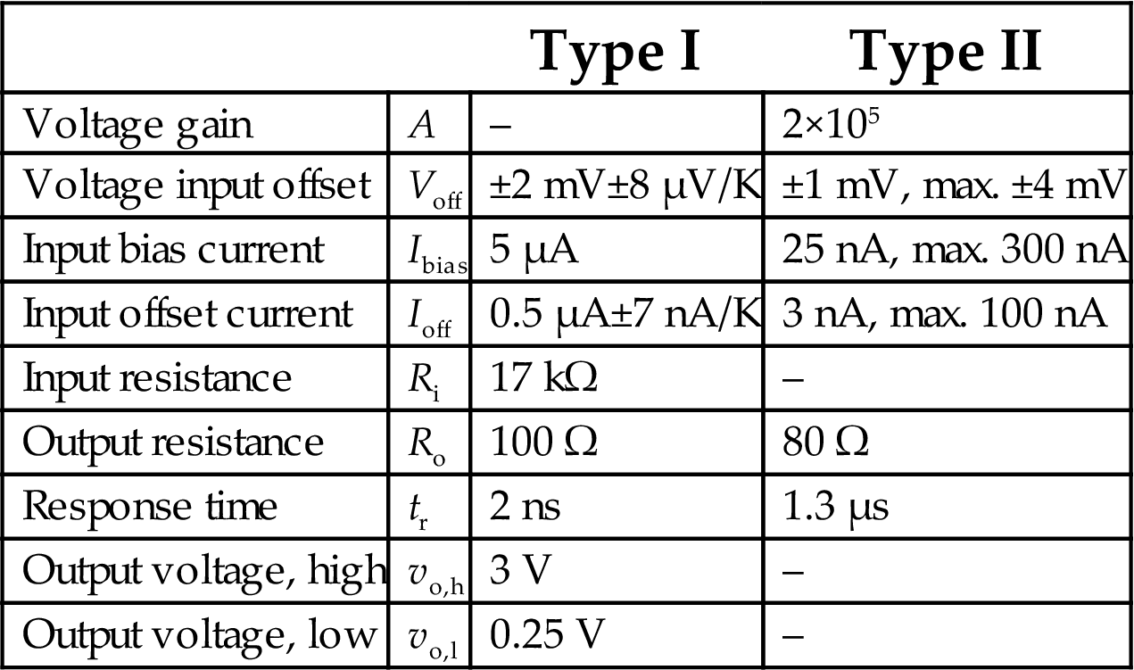
There are numerous types of operational amplifiers on the market with widely divergent specifications, and for a broad spectrum of applications. Table C.1 shows the major specifications for three types of operational amplifiers: types I and II are general purpose low-cost operational amplifiers, one with bipolar transistors at the input side (type I) and the other with JFETs at the input (type II). Type III is designed for high-frequency applications, with MOSFET transistors at the input. Also included are the temperature coefficient (tc) of the offset voltage, the CMRR, the supply voltage rejection ratio (SVRR), the slew rate, the DC gain A0 and the unity gain bandwidth ft.
Table C.1

In the analysis that follows we distinguish two types of errors: additive and multiplicative errors. Offset and bias currents cause additive errors. Multiplicative errors are caused by the finite gain and the first-order frequency dependence of the gain; in the analysis of the frequency dependence it is assumed that the DC loop gain is much larger than unity: A0β![]() 1.
1.
For a number of interface circuits we give, without any further derivation, their performance in terms of transfer function and input resistance, taking into account the nonideal behavior of the operational amplifier. Knowing the input impedance of an interface circuit, the error due to loading the sensor can easily be estimated.
C.2 Current-to-voltage converter
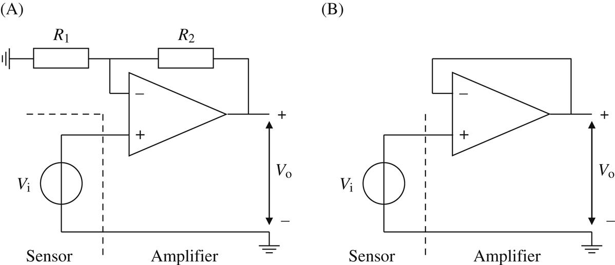
Most AD converter types require an input voltage with a range from 0 to the ADC’s reference voltage. When the ADC converts the output of a sensor with current output (such as a photo detector), that current must first be converted into a proper voltage that matches the ADC’s input range. The basic configuration that accomplishes this task is given in Fig. C.2A.

Assuming the operational amplifier has ideal properties, the transfer of this I–V converter is simply Vo=−IiR and the input resistance is zero. The bias current of the operational amplifier sets a lower limit to the input range, the supply voltages an upper limit. The transfer including additive errors results in:
(C.1)
To reduce the effect of bias current, a current compensation resistance with value R is inserted in series with the noninverting input terminal (Fig. C.2B). The transfer becomes:
(C.2)
which shows that current compensation reduces the error due to the bias current by about a factor of 5 (see Table C.1). The transfer including multiplicative errors due to finite gain A0 is:
(C.3)
which means that the scale error is about the inverse of the DC gain of the amplifier. The first-order approximation of the transfer of an operational amplifier is:
(C.4)
with τA the first-order time constant of the amplifier. Amplifiers with this transfer have a constant gain-bandwidth product: in feedback mode, the overall gain decreases as much as the bandwidth increases. At unity gain the bandwidth equals the “unity gain bandwidth” which is the value specified by the manufacturer, as in Table C.1. Apparently ft=ωt/2π=A0/2πτA. Taking this into account the transfer of the I–V converter is:
(C.5)
Note that the bandwidth of the converter equals the unity gain bandwidth of the operational amplifier. The input resistance in terms of input admittance results in:
(C.6)
In general, 1/Ri![]() A0/R so the input impedance Rin=1/Gin is about R/A0; in most cases a sufficiently low value to guarantee that the whole input current flows through the feedback resistor.
A0/R so the input impedance Rin=1/Gin is about R/A0; in most cases a sufficiently low value to guarantee that the whole input current flows through the feedback resistor.
C.3 Noninverting amplifier
With a voltage amplifier the output voltage range of a sensor can be matched to the input range of an ADC. Voltage amplification is accomplished by either an inverting or a noninverting amplifier configuration, depending on the required signal polarity. Fig. C.3A shows a noninverting amplifier with gain 1+R2/R1 and infinite input resistance. Hence the gain can be arbitrarily chosen by the two resistances, and the sensor experiences no electrical load. For R2/R1=0, the configuration is called a buffer (Fig. C.3B).
In the following formulas the feedback portion R1/(R1+R2) is abbreviated by β according to the notation in Chapter 3, Uncertainty aspects. For the buffer amplifier, β=1 (unity feedback). The transfer of the noninverting amplifier including additive errors equals:
(C.7)
The lower limit of the signal voltage range is set mainly by the offset voltage and to a lesser degree the bias current. After nullifying the offset, it is the temperature dependency of the offset that limits the range. The transfer shows a scale error (multiplicative error) due to the finite gain:
(C.8)
The scale error is the inverse of the loop gain A0β. Taking into account the frequency-dependent gain as in Eq. (C.4), the transfer of the noninverting amplifier is:
(C.9)
Obviously the bandwidth is proportional to β, and the transfer is inversely proportional to β. Hence the product of gain and bandwidth has a fixed value: the gain-bandwidth product. This relationship is shown in Fig. C.4.

Numerical example. A0=104, β=0.01, so A0β=100; unity gain bandwidth A0/τA=106 rad/s, so the operational amplifier’s cutoff frequency is 1/τA=100 rad/s and the noninverting amplifier bandwidth is 104 rad/s.
Fig. C.5 shows a simulation1 of the transfer characteristic using a general purpose, low-cost operational amplifier for three gain factors: 1 (buffer), 100 and 10,000. Clearly the product of gain and bandwidth is constant. At higher frequencies the second-order behavior of the operational amplifier becomes apparent.

Finally, the input resistance of the noninverting amplifier is found to be:
(C.10)
which is sufficiently high in most applications.
C.4 Inverting amplifier
Fig. C.6 shows the inverting amplifier configuration. Its voltage transfer is –R2/R1 and the input resistance is R1, a much lower value than in the case of the noninverting amplifier.

The transfer including additive errors amounts:
(C.11)
The contribution of the bias current Ib− can be reduced by inserting a resistance R3 in series with the noninverting input terminal, with a value equal to R1//R2, that is the parallel combination of R1 and R2. With this bias current compensation, the term Ib− in Eq. (C.11) is replaced by Ioff.
The transfer including multiplicative errors due to a finite gain is:
(C.12)
which, again, introduces a scale error equal to the inverse of the loop gain. The frequency-dependent gain is given by
(C.13)
Here too, the product of gain and bandwidth is constant. The frequency characteristics are similar to those in Fig. C.4. The input resistance becomes:
(C.14)
a value that is almost equal to R1. Note that this value can be rather low, resulting in an unfavorable load on the transducer.
C.5 Comparator and schmitttrigger
C.5.1 Comparator
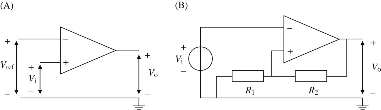
A voltage comparator (or short comparator) responds to a change in the polarity of an applied differential voltage. The circuit has two inputs and one output (Fig. C.7A). The output has just two levels: high or low, all depending on the polarity of the voltage between the input terminals. The comparator is frequently used to determine the polarity in relation to a reference voltage.
It is possible to use an operational amplifier without feedback as a comparator. The high gain makes the output either maximally positive or maximally negative, depending on the input signal. However, an operational amplifier is rather slow, in particular when it has to return from the saturation state. Table C.2 gives the specifications for two different types of comparators, a fast type and an accurate type.
Table C.2
Purpose-designed comparators have a much faster recovery time with response times as low as 10 ns. They have an output level that is compatible with the levels used in digital electronics (0 and +5 V). Their other properties correspond to a normal operational amplifier and the circuit symbol resembles that of the operational amplifier.
C.5.2 Schmitttrigger
A Schmitttrigger can be conceived as a comparator with hysteresis. It is used to reduce irregular comparator output changes caused by noise in the input signal. A simple Schmitttrigger consists of an operational amplifier with positive feedback (Fig. C.7B). The output switches from low to high as soon as Vi exceeds the upper reference level Vref1, and from high to low as soon as Vi drops below the lower level Vref2. For proper operation the hysteresis interval Vref1−Vref2 must exceed the noise amplitude. However, a large hysteresis will lead to huge timing errors in the output signal.
In Fig. C.7B a fraction β of the output voltage is fed back to the noninverting input: β=R1/(R1+R2). Suppose that the most positive output voltage is E+ (usually just below the positive power supply voltage) and the most negative output is E−. The voltage at the noninverting input will be either βE+ or βE−. When Vi is below the voltage on the noninverting input, then Vo equals E+ (because of the high gain). This remains a stable situation as long as Vi<βE+. If Vi reaches the value βE+, the output will decrease sharply and so will the noninverting input voltage. The voltage difference between both input terminals decreases much faster than Vi increases. So, within a very short period of time, the output becomes maximally negative E−. As long as Vi>βE−, the output remains Vo=E−, a new stable state.
The comparator levels of the Schmitttrigger are apparently βE+ and βE−. In conjunction with the positive feedback, even a rather slow operational amplifier can have a fast response time. Evidently, a special comparator circuit is even better. The switching levels can be adjusted by connecting R1 to an adjustable reference voltage source Vref instead to ground. Both levels shift by a factor VrefR1/(R1+R2).
C.6 Integrator and differentiator
Velocity information can be derived from an acceleration sensor (for instance a piezoelectric transducer) and displacement from velocity (for instance from an induction-type sensor) by integrating the sensor signals. The reverse is also possible, by differentiation, but this approach is not recommended because of an increased noise level. Basic integrator and differentiator circuits are shown in Fig. C.8. Ideally the transfers in time and frequency domains are given by:
(C.15)
(C.16)

However, these circuits will not work properly. The integrator runs into overload because the constant offset voltage and bias current will be integrated too. This is prevented by limiting the integration range, simply by adding a feedback resistor in parallel to the capacitance C. The differentiator is unstable because of the (parasitic) second-order behavior of the operational amplifier. This too is prevented by adding a resistor, in series with the capacitance C, resulting in a limitation of the differentiation range.
C.6.1 Integrator
Fig. C.9 shows the modified or “tamed” integrator. Taking into account the finite gain of the operational amplifier A, the transfer function of this integrator is:
(C.17)
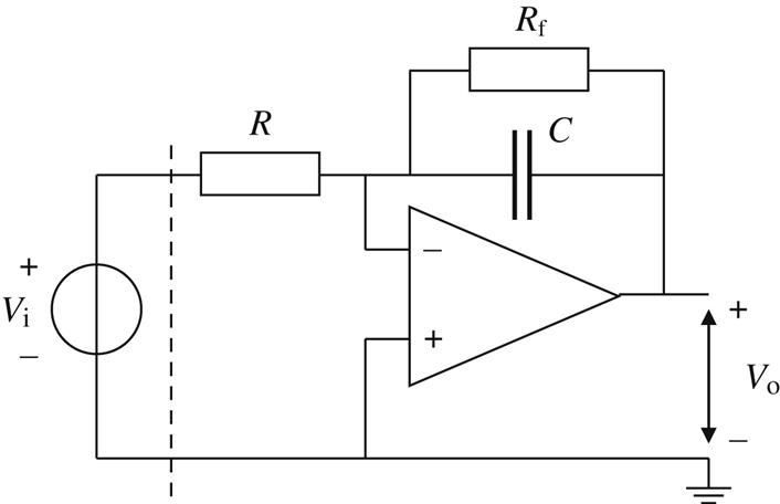
Assuming a frequency-independent amplifier gain: A=A0, the transfer function becomes:
(C.18)
The condition for the last approximation is valid for A0![]() 1 (which is always the case) and A0R
1 (which is always the case) and A0R![]() Rf (which is usually the case). The inclusion of resistance Rf limits the LF transfer to Rf/R, whereas the lower limit of the integration range is set to fL=1/(2πRfC).
Rf (which is usually the case). The inclusion of resistance Rf limits the LF transfer to Rf/R, whereas the lower limit of the integration range is set to fL=1/(2πRfC).
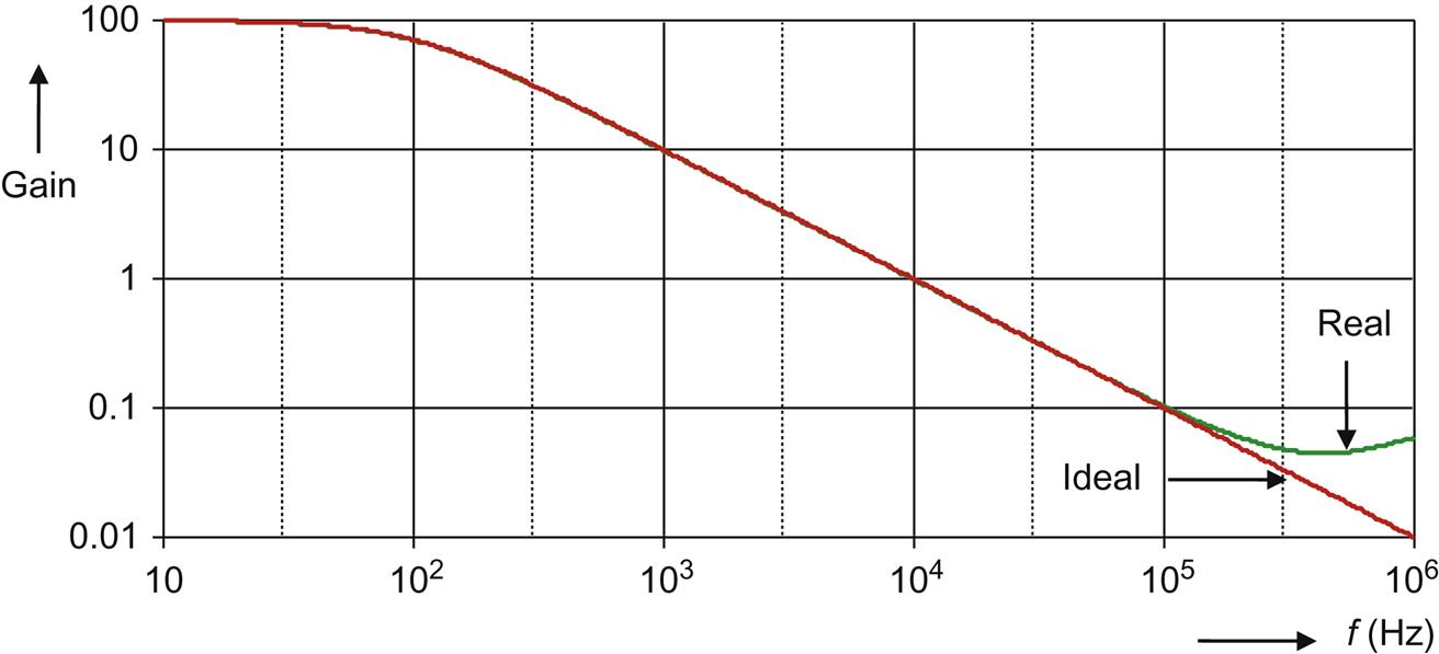
Numerical example. Assume that a lower limit of the integration range of 100 Hz and a DC gain of 100 are required. The component values should satisfy Rf/R=102 and RfC=1/200π, accomplished by, for instance Rf=100R=100 kΩ and C=16 nF. Fig. C.10 shows the frequency characteristic for this design, based on a simulation with an ideal and a real operational amplifier. Clearly the higher limit of the integration range is set by the frequency-dependent gain of the operational amplifier.
C.6.2 Differentiator
The transfer of the basic differentiator, taking into account the finite gain of the operational amplifier, is given by:
(C.19)
For A=A0 and A0![]() 1 this is:
1 this is:
(C.20)
This corresponds to a first-order high-pass characteristic with cutoff frequency at ω=A0/RC. The differentiation range is limited to this frequency. For much lower frequencies, the transfer function is just −jωRC and corresponds to that of an ideal differentiator.
However, when the frequency dependence of the operational amplifier gain according to Eq. (C.4) is taken into account, the transfer function becomes:
(C.21)
This characteristic shows a sharp peak at ω2τARC≈A0, for which value the transfer is about A0RC/(RC+τA).
Numerical example. The required gain is 0.1 at 1 rad/s. So the component values R and C should satisfy 1/RC=10 rad/s. Suppose the amplifier properties are: A0=105, unity gain bandwidth 105 rad/s. Fig. C.11 presents the calculated characteristic for this example. The transfer shows a peak of ≈104 at the frequency 103 rad/s.

Fig. C.12 shows a simulation for a general purpose operational amplifier with frequency compensation (i.e. it behaves almost as a first-order system). Component values in this simulation are R=100 kΩ, C=1 μF. Differences compared to Fig. C.11 are due to different amplifier parameters A0 and τA of the real amplifier.

If the operational amplifier has a second-order cutoff frequency (and most do have), instability may easily occur. Therefore the differentiating range should be limited to some upper frequency, well below the cutoff frequency of the operational amplifier. This is accomplished by inserting a resistor Rs in series with the capacitor C, as shown in Fig. C.13.
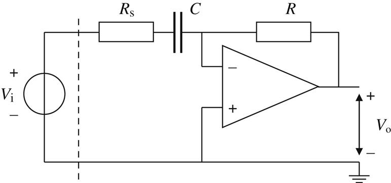
With the “taming resistor” Rs the transfer becomes:
(C.22)
Taking into consideration the finite and frequency-dependent gain of the operational amplifier according to Eq. (C.4) and assuming A0![]() 1, the transfer is modified to:
1, the transfer is modified to:
(C.23)
For R![]() Rs and RsC
Rs and RsC![]() (RC+τA)/A0 this can be approximated by:
(RC+τA)/A0 this can be approximated by:
(C.24)
Numerical example. Same values as for the uncompensated differentiator and Rs=R/100. The transfer is calculated from Eq. (C.24) and displayed in Fig. C.14. It shows that the peak is reduced by inserting resistance Rs. The differentiation range runs from very low frequencies up to about 1000 rad/s.

The simulation in Fig. C.15 shows the effect of a taming resistor, here 100 Ω. Note that the sharp peak has completely disappeared. Further, note the big difference between an ideal operational amplifier and a real type.

C.7 Filters
Removing unwanted signal components (noise, interference, intermodulation products, etc.) can be accomplished by (analogue) filters. Simple filters consist of passive components only. However, loading such filters (at both input and output) may easily affect the performance. In such cases active filters (with operational amplifiers) are preferred, providing independent choices for various filter parameters (input and output impedance, cutoff frequency, gain). The first-order integrator and differentiator of the preceding section are essentially a low-pass and a high-pass filter, respectively. Fig. C.16 shows an active band-pass filter.

Assuming ideal operational amplifier characteristics the transfer function is:
(C.25)
so this is is a combination of gain (−R2/R1), low-pass filter (fl=1/2πR2C2) and high-pass filter (fh=1/2πR1C1). Fig. C.17 shows the transfer function (frequency characteristic) obtained by simulation with an ideal and a low-cost operational amplifier. In this design, the pass-band gain is set to 100 and the high-pass and low-pass frequencies are set at 100 Hz and 1 kHz, respectively, a combination that can be obtained with the component values R1=1 kΩ, R2=100 kΩ, C1=1600 nF and C2=1.6 nF. Both curves are almost identical, since the unity gain bandwidth of the (real) operational amplifier is much higher than the filter gain over the whole frequency range.
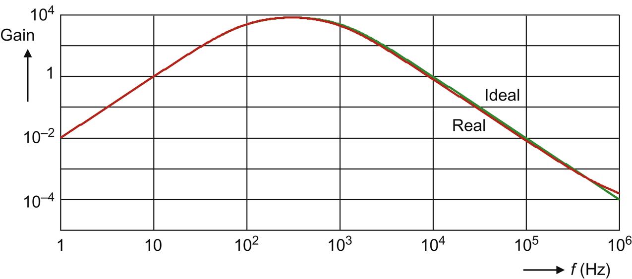
Fig. C.18 shows a second-order low-pass filter of the “Sallen-Key” configuration.
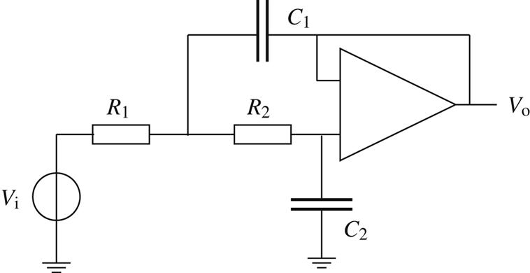
Its transfer function equals:
(C.26)
Under particular conditions for the resistance and capacitance values this filter has a Butterworth characteristic, which means a maximally flat amplitude characteristic in the pass-band. The general transfer function of a Butterworth filter of order 2n is:
(C.26)
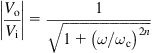 (C.26)
For n=1 the Butterworth condition is C1/C2=(R1+R2)2/2R1R2. When R1=R2=R, then C1=2C2. The cutoff frequency is fc=1/2πRC1. Fig. C.19 depicts a simulation of such a filter, with a cutoff frequency of 1 kHz (by making R1=1 kΩ and C1=160 nF).
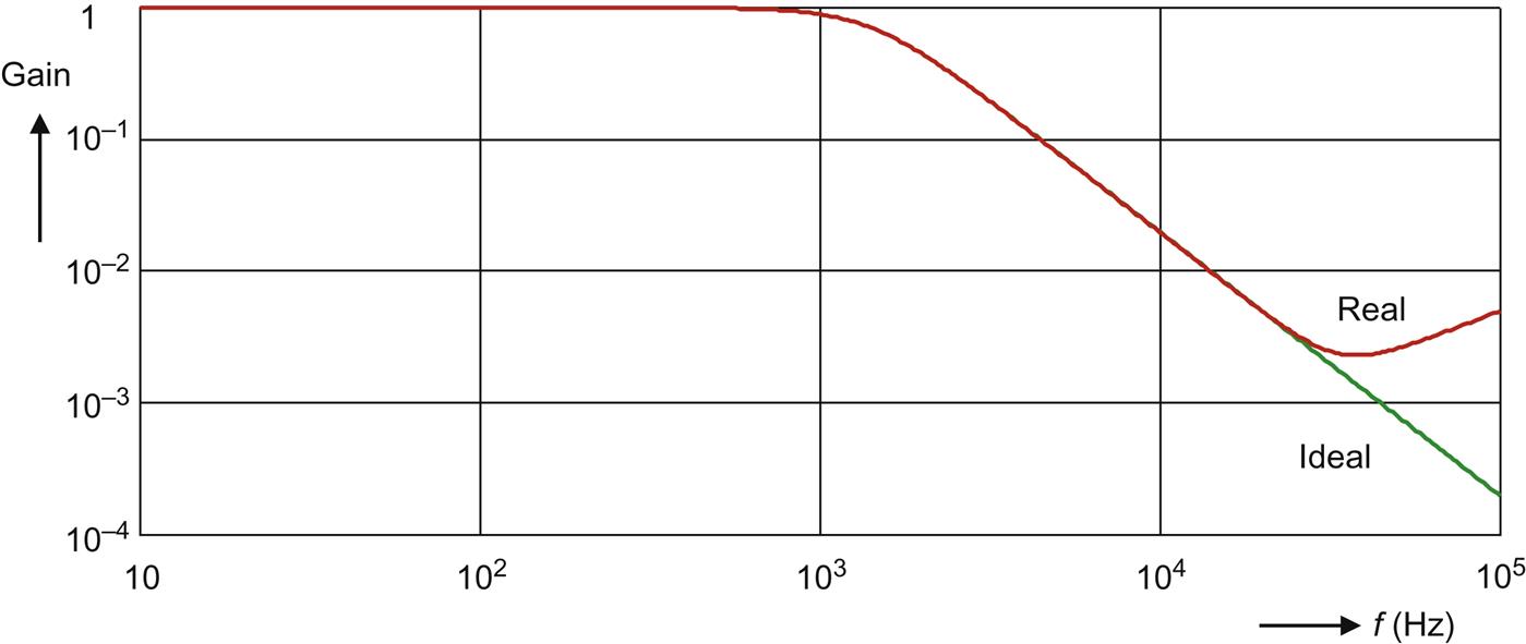
Here, the influence of the finite unity gain bandwidth of the operational amplifier is clearly visible and limits a proper filter function to about 20 kHz in this example.
The slope of the stop-band characteristic of a first-order low-pass filter is −6 dB/octave or −20 dB/decade. To obtain better selectivity, higher order filters can be obtained by simply cascading (putting in series) filters of lower order. The slope of the characteristic in the stop-band results in −6n dB/octave for a low-pass filter of order n. Note that the attenuation in the pass-band is also n times more compared to that of a first-order filter. For instance, cascading three second-order Butterworth filters of the kind shown in Fig. C.18 results in a slope of −36 dB/octave.