
Chapter 8. Low-Noise Amplifiers
8.1 Introduction
A low-noise amplifier is generally placed at the front end of a receiver and plays the role of amplifying received signals that are weak. As shown in Figure 8.1, the input signal of the low-noise amplifier consists of both signal Ps and noise Ns that are amplified together. The impedance Zo at the source and load has a typical value of 50 Ω, which is determined by a coaxial connector. In addition, the internal noise sources of the low-noise amplifier also contribute to output noise power No. As a result, the signal-to-noise ratio at the output is worse than that at the input. Thus, the low-noise amplifier should be designed so that its internal noise sources minimally contribute to the output noise power, and it should amplify the received signal to the extent that the next-stage signal processing components can process the signal.
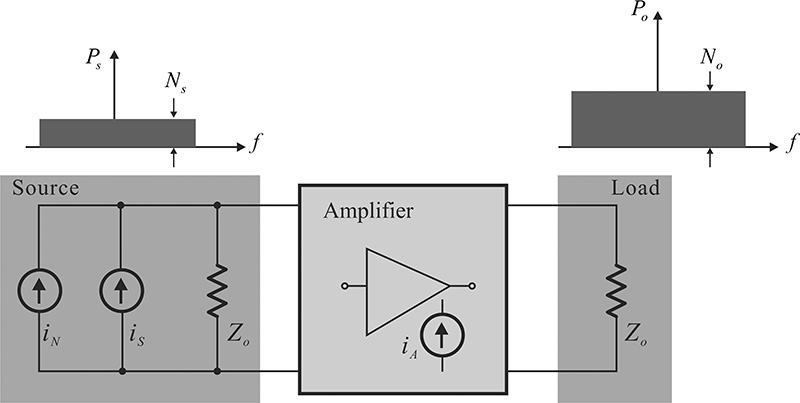
Figure 8.1 Low-noise amplifier design concept. The signal and noise powers Ps and Ns are represented by the current sources iS and iN, and Po and No are the delivered signal and noise powers to the load. The current source iA in the amplifier represents the amplifier’s internal noise source. The impedance Zo at the source and load side has a typical value of 50 Ω.
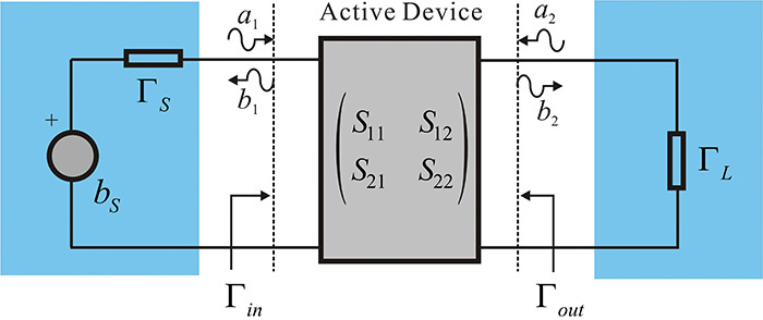
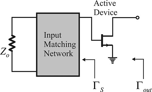
The amplifier shown in Figure 8.1 can be generally represented as shown in Figure 8.2. Thus, the design of a typical low-noise amplifier must address the problem of determining the impedance looking into the source and load from the active device. In this chapter, we will first explain the gain that is an important measure of a low-noise amplifier as a function of the source and load reflection coefficients, ΓS and ΓL, shown in Figure 8.2, and we will also look at the ΓS and ΓL that give maximum gain from a design perspective. However, in designing a low-noise amplifier, not only the gain but also the noise figure must be taken into consideration. We will discuss how to select ΓS and ΓL by considering the noise figure and gain.
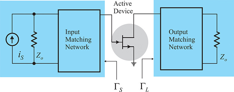
Figure 8.2 The definition of the source and load reflection coefficients ΓS and ΓL. Usually ΓS and ΓL are defined using the same reference impedance as those used for the S-parameters of the active device.
In addition, because the active device has some inherent degree of feedback, it shows a negative resistance for specific ΓS and ΓL, and because of this, the amplifier can turn into an oscillator. Therefore, the method for examining whether or not the active device yields a negative resistance at a given frequency will be presented, and then the method of stabilizing the active device in that situation will be explored.
8.2 Gains
8.2.1 Definition of Input and Output Reflection Coefficients
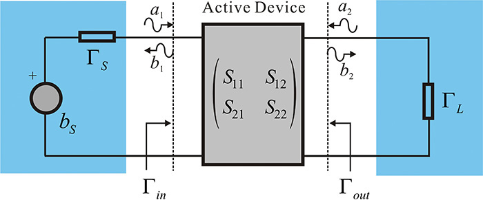
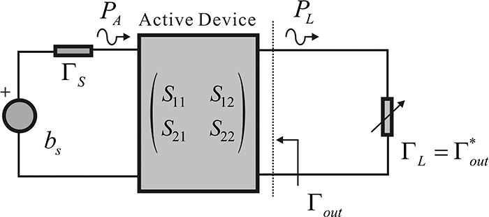
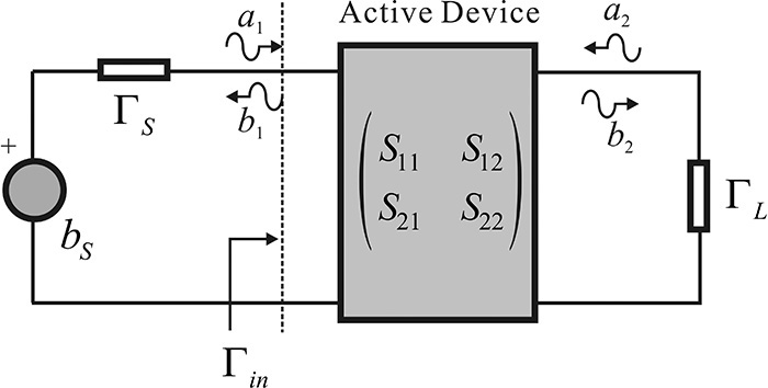
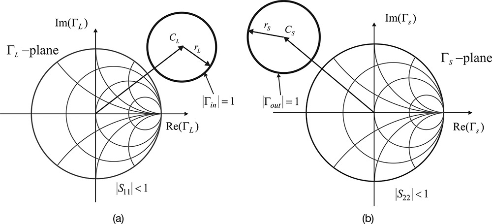
The source and load impedances are generally fixed as RS = RL = Zo. However, the optimum gain and noise figure of an active device are rarely obtained for the fixed source and load impedances RS = RL = Zo. The gain and noise figure of the active device depend significantly on the load and source impedances. Thus, the fixed-value source and load impedances should be converted into the appropriate impedances using the matching circuits. Due to the inclusion of the matching circuits, the active device generally sees the converted source and load impedances that are different from Zo. This is shown in Figure 8.3. Here, ΓS represents the reflection coefficient looking into the input matching circuit from the active device, while the reflection coefficient looking into the output matching circuit from the active device is denoted as ΓL. Note that the reference impedance is required in order to measure ΓS and ΓL, and it is assumed to be the same as the reference impedance used to measure the S-parameters of the active device.
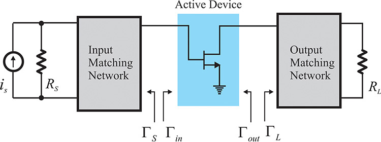
The reflection coefficient seen from the active device input when a load ΓL is connected to the active device output is denoted as Γin; similarly, the reflection coefficient seen from the active device output when a source ΓS is connected to the active device input is denoted as Γout. Therefore, using the S-parameters of the active device, the input and output reflection coefficients are expressed in Equations (8.1) and (8.2).
8.2.2 Thevenin Equivalent Circuit
Figure 8.4 shows a circuit for measuring the reflection coefficient of a Thevenin equivalent circuit, which is often used to represent a one-port network containing internal sources. In Figure 8.4, the Thevenin equivalent circuit is shown in the shaded area and has an open-circuit voltage ET and impedance ZT.
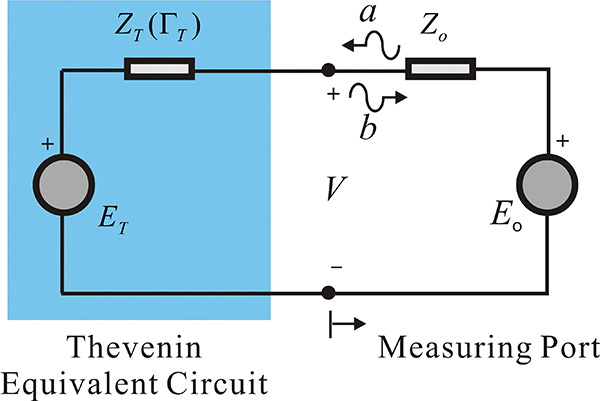
Figure 8.4 Wave representation of Thevenin equivalent circuit that has an open-circuit voltage of ET and impedance ZT. The measurement port has a voltage Eo and Zo.
The port is connected to the Thevenin equivalent circuit to measure its reflection coefficient. Here, Eo and Zo represent the port voltage and impedance, respectively. Using superposition, voltage V in Figure 8.4 can be determined as
Voltage V is the sum of the incident and reflected voltages as shown in Equation (8.3). The incident voltage is given by
Therefore, substituting Equation (8.4) into Equation (8.3), reflected voltage V– from Equation (8.3) is given by
Expressing reflected voltage V– in Equation (8.5) in terms of a normalized incident and reflected voltages a and b, we obtain Equations (8.6) and (8.7).
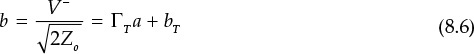
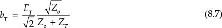
Reflected voltage b in Equation (8.6) consists of two terms. The first term is the reflection coefficient looking into the Thevenin circuit when ET = 0. The second term is the reflection coefficient that depends on the voltage source ET that can be interpreted as the voltage appearing across the port impedance Zo when Eo = 0. In circuit theory, ET is determined by measuring the open-circuit voltage of a one-port network. Similarly, impedance ZT is obtained by measuring the impedance of the one-port network with all the internal sources in that network turned off. The reflection coefficient given by Equation (8.6) corresponds to this circuit theory. The reflection coefficient ΓT is obtained by measuring the reflection coefficient with source ET turned off. Similarly, the reflection coefficient due to source ET is found by measuring the voltage delivered to the port impedance Zo instead of measuring the open-circuit voltage. The sum of the two reflections constitutes the total reflection in Equation (8.6). The difference is in measuring the internal source contribution by using a termination Zo instead of an open circuit.
Prove that, |bT|2, obtained from Equation (8.7), is the power delivered to the port resistance Zo when Eo = 0.
Solution
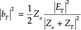
Because
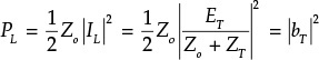
it can be seen that PL = |bT|2.
Now, the amplifier in Figure 8.3 can be represented by the simple schematic that uses the Thevenin equivalent circuit shown in Figure 8.5. The input can be represented by the Thevenin equivalent circuit, while the output can be represented by a simple load. The active device is represented by the S-parameters, and the incident and reflected voltages (a1, a2) and (b1, b2) are defined using the reference impedances that measured the S-parameters of the active device.
Next, we examine the power delivered to the load when a source represented by a Thevenin equivalent circuit is connected to an arbitrary load ΓL, as shown in Figure 8.6. Note that both the reflection coefficients of the load and source represented by the Thevenin equivalent circuit are measured based on the same reference impedance Zo.
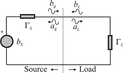
Figure 8.6 The circuit where the source is connected to the load. The source and load reflections are measured using the same reference impedances.
From Equation (8.6), the reflected voltage bg toward the load in Figure 8.6 is expressed in Equation (8.8)
while the reflected voltage from the load is shown in Equation (8.9).
Since bg = aL, and ag = bL, the incident voltage toward the load aL can be obtained from Equations (8.8) and (8.9), as shown in Equation (8.10).
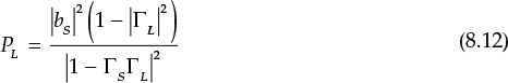
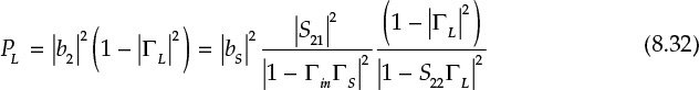
Thus, the power delivered to the load is
Substituting Equation (8.10) into Equation (8.11), PL can be expressed with Equation (8.12).
In addition, the available power from the source is delivered to the load when the source and the load impedances are conjugate matched, that is, when ΓS = (ΓL)*. Substituting ΓS = (ΓL)* into Equation (8.12),
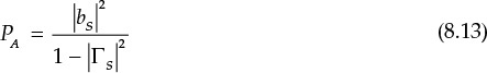
To verify that the result given by Equation (8.13) is the available power, Equation (8.7) is substituted into Equation (8.13), and the manipulation of PA results in
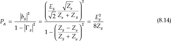
We can see that PA in Equation (8.14) is equal to the available power that can be obtained from the source having internal resistance ZS. This is expressed in Equation (6.5) of Chapter 6. In addition, using Equations (8.12) and (8.13), the ratio of power delivered to the load to available power can be computed as
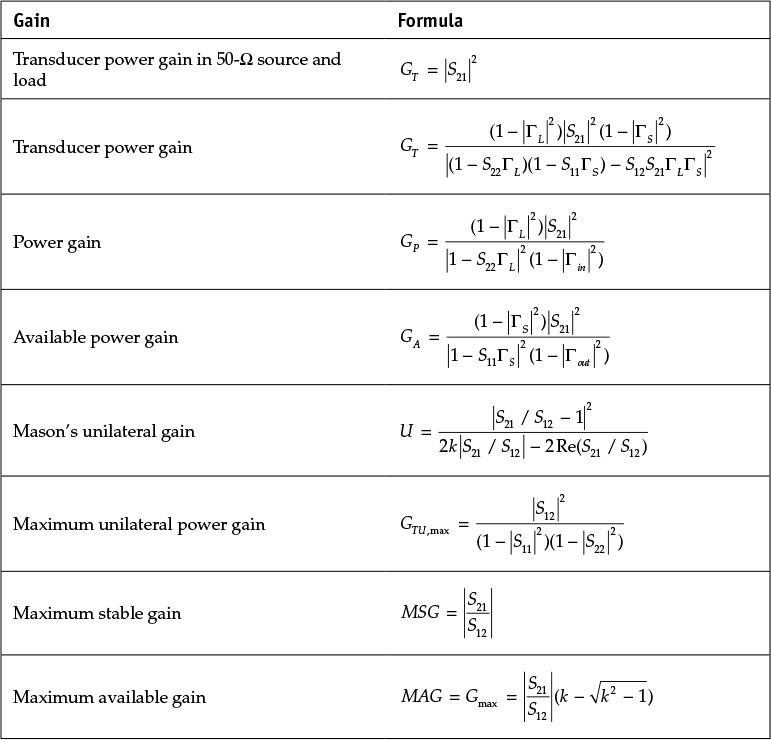
8.2.3 Power Gains
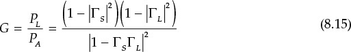
Gain is one of the key performance indicators for amplifiers and is defined in various ways depending on measurement and design purposes. Among these gains is the transducer power gain that is frequently used in measurements and is defined in Equation (8.16).
In measuring the transducer gain, the available power from a source with a 50-Ω internal resistance is measured by connecting a power meter (with a 50-Ω internal resistance) to the source. Then, inserting the amplifier between the meter and the source, and measuring the delivered power to the power meter, the ratio of power delivered to the load to available power can be obtained and the ratio can be interpreted as the transducer gain given by Equation (8.16).
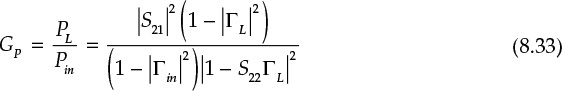
On the other hand, from a design perspective, when the output impedance of the amplifier is conjugate matched by varying the load impedance, the available power at the output can be obtained. The ratio of the available output power to the available power from the source is called available power gain and is defined in Equation (8.17).
Using the simplified schematic shown in Figure 8.7, the available power gain GA is found to be equal to the ratio of PL/PA. Since the input matching network is assumed to be lossless, the available power from the active device input is equal to that from the source. In addition, the tuning of the load impedance for the maximum power delivery is equivalent to the tuning of ΓL. Thus, the available power gain is equal to PL/PA.
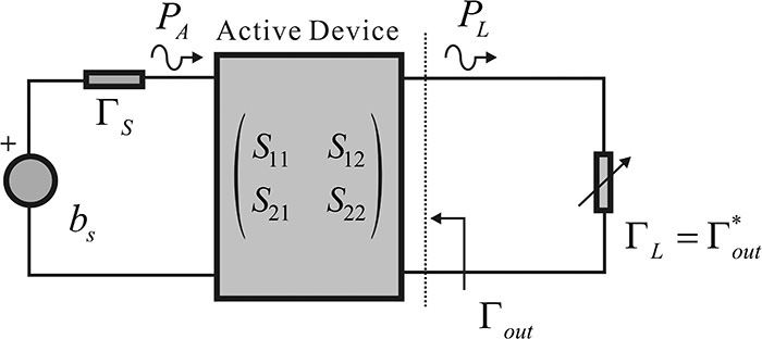
Figure 8.7 The concept of available power gain. The load ΓL is tuned for the maximum power delivery and the available power gain is then the ratio of PL/PA at the maximum power delivery.
The available power gain is the maximum gain derived from the output for a given source impedance, which is a function of the source impedance only. Therefore, the available power gain represents the degradation of the gain due to the fixed source impedance.
Based on the symmetrical concept for a fixed load, when the source impedance is adjusted to deliver maximum power to the load as shown in Figure 8.8, then the ratio of the input power to the delivered load power is called power gain. Using the simplified schematic, power gain can be defined as
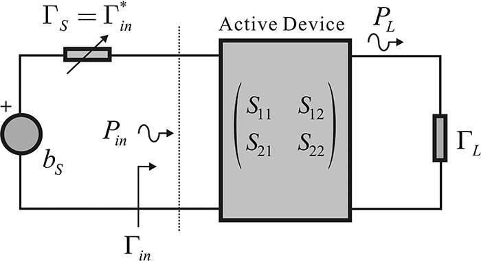
Figure 8.8 The concept of power gain. The source is tuned for the maximum PL. The power gain is the ratio of PL/Pin at the maximum PL.
The power gain, as an indicator of the degradation of the gain due to a chosen fixed load, is commonly used in design. The previous three power gains can be expressed in terms of the two-port S-parameters and the source and load reflection coefficients or impedances at the device plane. This will be discussed further in the next section.
8.2.3.1 Transducer Power Gain
Figure 8.9 shows again a simplified schematic representation of the amplifier.
In Figure 8.9, the one-port circuit seen from the load ΓL can be represented by the Thevenin equivalent circuit that includes the active device and the input circuit, and the previously developed power relationship in Equations (8.13) and (8.15) can be applied. At the device output plane, the Thevenin reflection coefficient ΓT is shown in Equation (8.18).
The Thevenin reflected voltage bT is the reflected voltage that appears across the reference impedance Zo when the load ΓL is replaced by Zo. From Figure 8.10, bT is given by Equation (8.19).
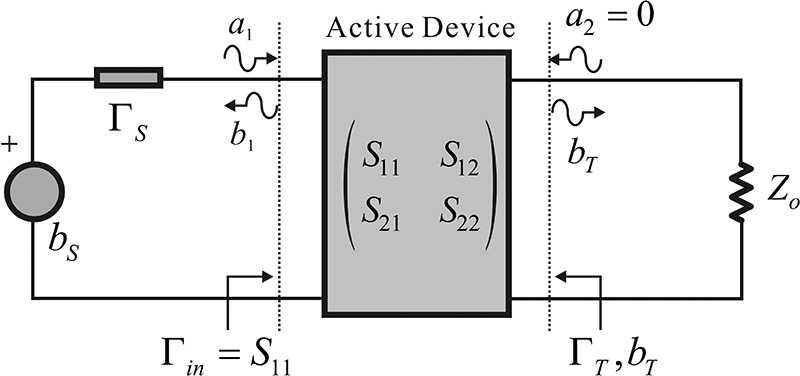
Note that Γin = S11 because a2 = 0. Applying Equation (8.10), a1 is given by
Thus, from Equation (8.20), the Thevenin reflected voltage bT is shown in Equation (8.21).
Therefore, the equivalent circuit seen from the load ΓL can be represented as shown in Figure 8.6.
Applying Equation (8.12), the power delivered to the load ΓL is given by Equation (8.22).
Since the available power from the source is the same as in Equation (8.13), the transducer power gain GT is expressed as
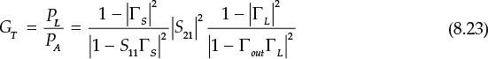
The transducer gain in Equation (8.23) is derived at the device output plane, but it can also be derived at the device input plane. The derived transducer gain is expressed as
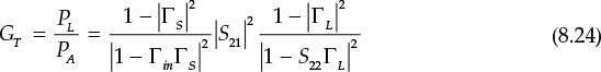
Although GT in Equation (8.24) is different from that in Equation (8.23), GT in Equation (8.24) is the same as that in Equation (8.23).
8.2.3.2 Available Power Gain
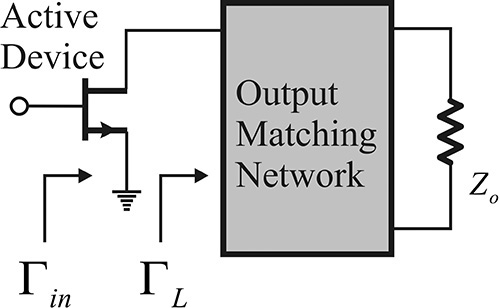
Available power gain is defined as the ratio of available power at the device input to available power at the output. Figure 8.11 again shows how to derive the available power gain, which is accomplished by using the previously derived transducer power gain.
Note that the transducer power gain is defined in terms of the available power at the input and the delivered power to the load. The available power at the output is the power when the load impedance is conjugate matched to Γout, as shown in Figure 8.11. This condition is ΓL = (Γout)*. Then, the available power gain can be obtained by substituting ΓL = (Γout)* into the transducer gain in Equation (8.23). Therefore, the available power gain is given by Equation (8.25).
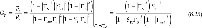
The available power gain can also be interpreted as the maximum gain for a fixed ΓS.
8.2.3.3 Power Gain
The power Pin delivered to the input of the device shown in Figure 8.12 is given by Equation (8.26).
Using Equation (8.10), Pin results in Equation (8.27).
In addition, a1 and a2 in Figure 8.12 are given by
Substituting a1 and a2 of Equations (8.28) and (8.29) into b2 gives Equation (8.30).

Then, b2 can be computed as Equation (8.31).
Thus, the power delivered to the load is given by Equation (8.32).
Therefore, based on the definition of power gain, the ratio of the input power Pin to the power delivered to the load PL is given by Equation (8.33).
The power gain is the ratio of input power to the power delivered to the load. However, the power gain can be interpreted in another way. The maximum power is delivered to the device’s input when the source impedance is conjugate matched to the device’s input impedance. The ratio of the input power at the conjugate matching condition to the power delivered to the load leads to the same result given by Equation (8.33). This is found in problem 8.4 at the end of this chapter. Thus, another way of interpreting the power gain is that it represents the maximum gain of the active device for a specific fixed load ΓL.
8.2.3.4 Unilateral Gain
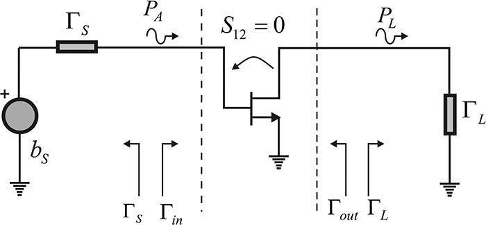
In general, S12 ≠ 0 and the active device has some feedback. However, S12 can generally be made 0 by adding the appropriate feedback circuit. In this case, there will be no feedback from output to input. This condition is then said to be unilateral. The resulting gain is called Mason’s gain, U, which is expressed in Equations (8.34a) and (8.34b).
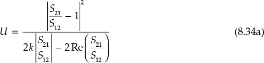
Since Mason’s gain is the gain measured after the active device has been completely stabilized by removing feedback, it can be considered as the true gain of the active device. Therefore, it is used as the criterion for determining whether a measured device at an arbitrary frequency is active or passive.
Since S12, which represents the feedback from output to input, is generally less than 1, a unilateral approximate expression for the transducer gain is often used in amplifier design and active device assessment. To obtain the unilateral transducer power gain, S12 = 0 is substituted into Equation (8.25). In this case, since Γin = S11 and Γout = S22, the transducer power gain is expressed in Equation (8.35).
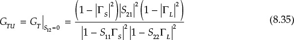
When the input and output reflection coefficients in Figure 8.13 are each conjugate matched (ΓS = (Γin)*, ΓL = (Γout)*), maximum gain is then obtained and the maximum unilateral gain GTU,max is shown in Equation (8.36).
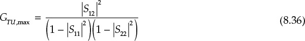
The calculation of the unilateral gain in Equation (8.35) is simple compared to the computations for other gains and it was commonly used in the past to evaluate the maximum gain of active devices when computers were not readily available.
8.3 Stability and Conjugate Matching
Active devices generally have feedback from output to input, however small. Due to this feedback, some load impedance values yield a negative resistance at the input. Similarly, a negative resistance can appear at the output for some values of the source impedance. When the negative resistance at the input or output appears at certain out-of-band frequencies, a designed amplifier may turn into an oscillator. In the case that the negative resistance appears at in-band frequencies, it limits the matching of an amplifier and must be eliminated through a stabilization method. For a stabilized device, the maximum gain occurs at the source and load impedances of the conjugate matching. In this section, we will discuss how to find the stable regions of the source and load impedances, and the mathematical derivation of the conjugate matching source and load impedances.
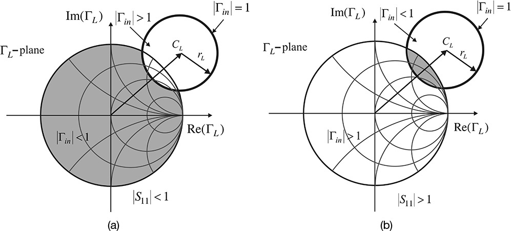
8.3.1 Load and Source Stability Regions
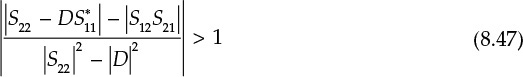
The input or output impedances of an active device may have a negative resistance for a particular load or source impedance, so the region of the load and source impedances that induce a negative resistance must first be found. When a negative resistance is induced at the input or output of an active device, the magnitude of the input or output reflection coefficients are mathematically greater than 1. That is, |Γin| > 1 and |Γout| > 1. Therefore, the problem of finding the stability regions requires determining two conditions:
1. A region of ΓL that gives |Γin| ≤ 1; and
2. A region of ΓS that gives |Γout| ≤ 1.
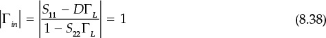
Condition 1 limits the range of load selection and is called the load stability region, and condition 2 limits the range of source selection and is thus called a source stability region. After determining the locus of the boundary (|Γin| = 1 and |Γout| = 1), the locus divides a region of ΓL or ΓS into two regions. Once a stable region is found between those two regions, the remaining region becomes automatically unstable, which gives rise to a negative resistance. From Figure 8.14, the input reflection coefficient is expressed by Equation (8.37)
where D = S11S22 – S21S12.
The reflection coefficient Γin for the impedance of a passive device satisfies |Γin| ≤ 1. However, for the impedance that has a negative resistance, |Γin| > 1. From Equation (8.37), ΓL that satisfies |Γin| = 1 is
Multiplying both sides of Equation (8.38) by |S22/D| and rewriting, the following expression is obtained:
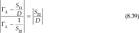
Equation (8.39) can also be represented as Equation (8.40).
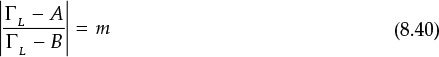
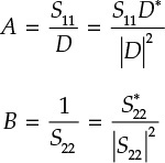
Constants A and B represent two points on the ΓL plane and are expressed as follows:
From Equation (8.40), m represents the ratio of the distances from a point ΓL to two points, A and B. The locus satisfying Equation (8.40) is well-known and is represented by the circle shown in Figure 8.15. The internal (I) and external (E) division points with the division ratio m:1 can be obtained from points A and B. The center of the circle becomes their midpoint between I and E. Half of the distance between points I and E becomes the radius of the circle.
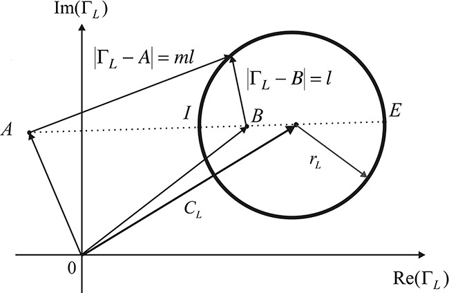
Points I and E are determined as
The center of the circle CL and the radius rL are then determined from points I and E as
Substituting A, B, and m into Equations (8.41a) and (8.41b), the center CL and the radius rL in the ΓL plane are given by
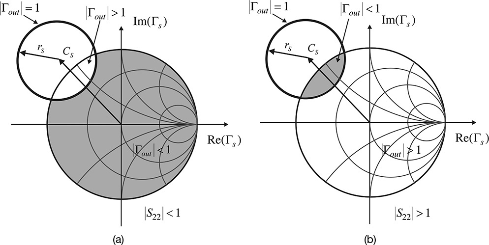
Load stability circles drawn using Equations (8.42a) and (8.42b) are shown in Figure 8.16. In order to determine the region of stability between the two regions divided by the load stability circle, one test point is necessary. The load of ΓL = 0 provides a good test point. Setting ΓL = 0 results in the input reflection coefficient Γin = S11. If |S11| < 1, it implies that |Γin| < 1 for ΓL = 0. Since |Γin| < 1 for ΓL = 0, the stable region is located inside the unit Smith-chart circle that includes the origin, as shown in Figure 8.16(a). Otherwise, the region that includes the origin is unstable.
Similarly, the region of ΓS giving |Γout| < 1 can be determined. The output reflection coefficient Γout in Figure 8.17 is expressed as

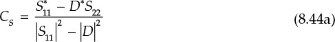
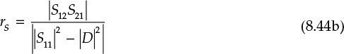
If Γout is set to |Γout| = 1, the source stability circles can be determined. Equation (8.43) can be obtained when the subscripts 1 and 2 in Equation (8.37) are interchanged. Therefore, by interchanging those subscripts in Equation (8.42), the center CS and radius rS of the source stability circle giving |Γout| = 1 in the ΓS–plane are given by Equations (8.44a) and (8.44b).
The stability circles drawn with the center CS and radius rS are shown in Figure 8.18 and, similar to our reasoning in the case of the load stability circle, when |S22| < 1, the region inside the unit Smith chart that includes the origin is the stable region shown in Figure 8.18(a). Otherwise, the region that includes the origin is the unstable region. In Figures 8.18(a) and (b), the resulting stable regions inside the unit Smith chart are represented by the shaded area.
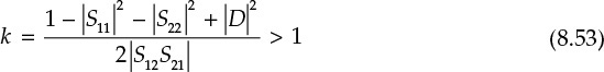
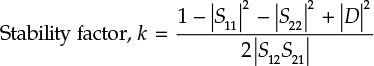
8.3.2 Stability Factor
From Figures 8.16(a) and 8.18(a), in order for the entire region |ΓS| ≤ 1and |ΓL| ≤ 1 on the Smith chart to be the region of stability, Equations (8.45) and (8.46) should be satisfied from Figure 8.19.
Substituting the center and radius of the load stability circle obtained from Equation (8.42) into Equation (8.45), we obtain
Equation (8.47) can be rewritten as Equation (8.48).
Expanding Equation (8.48), we obtain Equation (8.49).
Note that the following identity holds:
Squaring each term of Equation (8.49) and substituting Equation (8.50) into Equation (8.49), and then rewriting, Equation (8.51) is obtained.

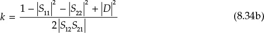
Thus, the necessary condition for Equation (8.51) is
Dividing both sides of Equation (8.52) by 2|S12S21| yields the stability factor k, which is used to examine the unconditional stability of the two-port network, as shown in Equation (8.53).
The other required condition can be obtained from Figures 8.16(b) and 8.18(b). The radius is large enough to include the Smith chart. The condition is rL – |CL| > 1. Substituting the center and radius results from Equation (8.42) into this condition gives Equation (8.54).
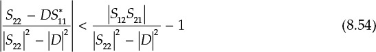
This requires that the right-hand side of the equation be positive, which is expressed in Equation (8.55).
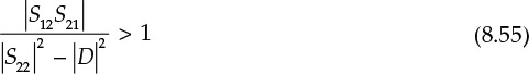
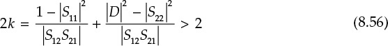
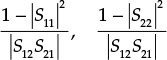
is obtained. However, since the second term of Equation (8.56) is less than 1, from Equation (8.55), the first term must be greater than 1. Therefore,
Equation (8.57) is an additional condition that must be satisfied. In addition, from the source stability circles, the following condition is obtained with Equation (8.58):
In conclusion, the necessary and sufficient conditions for the unconditional stability of a two-port circuit are expressed in Equations (8.59a)–(8.59c).
These are the three conditions that must be simultaneously satisfied.
Using the 3 V, 10 mA S-parameters of the FHX35LG/LP in ADS, plot the stability factor k and the following terms for the frequency range of 1–18 GHz:
Draw the source and load stability circles at 1 GHz.
Solution
Set up the circuit as shown in Figure 8E.1 using the two-port S-parameters of the ADS FHX35LG/LP. Perform the simulation and enter the equations in the display window to plot the stability factor and the two terms as shown in Measurement Expression 8E.1. The plot is shown in Figure 8E.2.
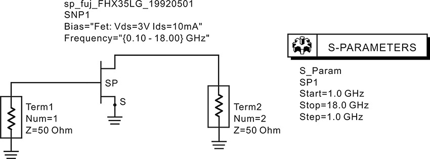
Figure 8E.1 Circuit for determining the stability of FHX35LG/LP. SNP1 is the data component and the DC bias circuit is not necessary.
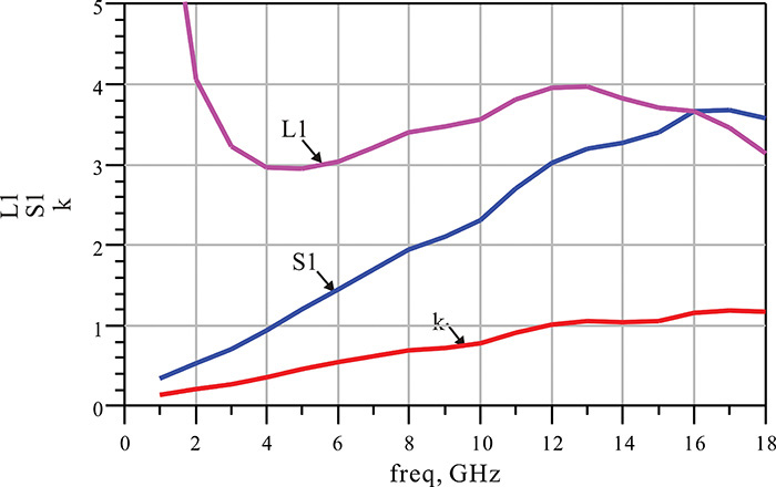
Figure 8E.2 Simulation results. The stability factor k is the smallest of the stability factors L1, S1, and k. Thus, the stability can be determined using k alone.
In Figure 8E.2, S1 and L1 are observed to be greater than k. Since the two terms are mostly greater than k, the stability factor k is critical to determining the stability of the circuit. The relationship that S1 and L1> k is generally true. In addition, as can be seen from the figure, above the 12-GHz frequency, k > 1 and the device is found to be stable while it is unstable at frequencies lower than 12 GHz.
![]() S1=(1-(mag(S11))**2)/(mag(S12*S21))
S1=(1-(mag(S11))**2)/(mag(S12*S21))
![]() L1=(1-(mag(S22))**2)/(mag(S12*S21))
L1=(1-(mag(S22))**2)/(mag(S12*S21))
Measurement Expression 8E.1 Equations for stability in the display window
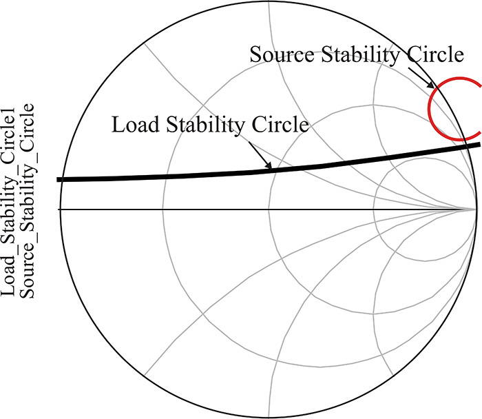
Since k < 1 at a frequency of 1 GHz, the device is found to be unstable at 1 GHz. In order to find the stable region, the equations in Measurement Expression 8E.2 are also entered in the display window to plot the load and source stability circles at 1 GHz.
![]() Source_Stability_Circle=s_stab_circle(S[0], 51)
Source_Stability_Circle=s_stab_circle(S[0], 51)
![]() Load_Stability_Circle=l_stab_circle(S[0],51)
Load_Stability_Circle=l_stab_circle(S[0],51)
Measurement Expression 8E.2 Equations for drawing the stability circles
The function s_stab_circle(S[0], 51) is the function for drawing the source stability circle given by Equation (8.44). The S-parameter index is set to [0] for the selection of S-parameters at a frequency of 1 GHz. The number 51 at the end represents the number of points used in plotting the circle. Similarly, l_stab_circle(S[0],51) is a function for plotting the load stability circle. The circles plotted on the Smith chart using these functions are shown in Figure 8E.3, where it can be seen that since |S11| < 1 and |S22| < 1, the region including the origin of the Smith chart is the region of stability.
8.3.3 Conjugate Matching
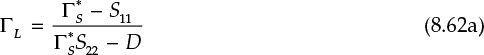
Figure 8.20 shows the amplifier whose input and output are conjugate matched. The objective of conjugate matching is to obtain maximum gain from the active device. When the input is conjugate matched, maximum available power is transferred from the source to the input of the active device. Simultaneously conjugate matching the output ensures that the maximum power that is amplified by the active device is delivered to the load. Therefore, maximum gain is obtained when the input and output are conjugate matched as shown in Equations (8.60a) and (8.60b).


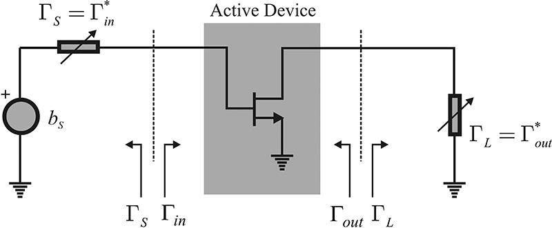
Figure 8.20 Simultaneous conjugate matching conditions. When ΓS = (Γin)* and ΓL = (Γout)*, the maximum gain occurs.
Equations (8.61a) and (8.61b) are obtained by rewriting Equations (8.60a) and (8.60b).
To solve the simultaneous equations, ΓL is expressed in terms of ΓS using Equation (8.60a) and vice versa, which yields
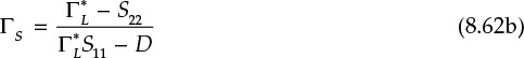
Substituting Equation (8.62a) into Equation (8.61a) and manipulating the results in the quadratic equation of ΓS as shown in Equation (8.63),
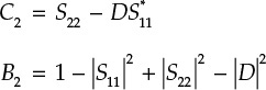
where
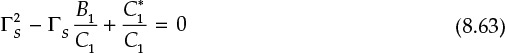
The solution to this quadratic equation is obtained in Equation (8.66).
Here, B1/(2|C1|) is a real number and can be expressed as shown in Equation (8.67).
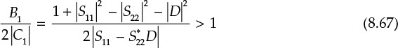
The term B1/(2|C1|) is greater than 1 when k > 1. To prove this, the denominator is expressed as shown in Equation (8.68).
Squaring the right-hand side of Equation (8.67) and using Equation (8.68) gives Equation (8.69).
This can be simplified into Equation (8.70).
Making use of the identity (a + b)2 – 4ab = (a – b)2 and rewriting Equation (8.70) yields Equation (8.71).
Thus, B1/(2|C1|) is greater than 1 when k > 1.
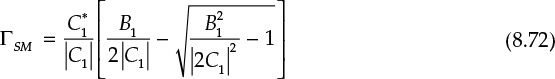
This implies that when the transistor is stable, that is, when k > 1, the term inside the square root is positive. In the selection of the sign of the square root in Equation (8.66), the sign must be selected such that |ΓSM| ≤ 1 because ΓSM cannot be implemented using a passive circuit for |ΓSM| ≥ 1. Since the magnitude of (C1)*/C1 outside the bracket [•] in Equation (8.66) is 1, the terms in the bracket [•] must therefore be less than 1. The terms in the bracket [•] can be considered in the form x – (x2 – 1)½ and x + (x2 – 1)½. The term x + (x2 – 1)½ becomes greater than 1 for x ≥ 1. Therefore, the realizable solution of ΓSM with a passive circuit is expressed in Equation (8.72).
Similarly, ΓLM can be obtained as shown in Equation (8.73)
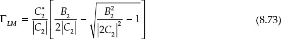
where
When k < 1, |ΓSM| = 1 and |ΓLM| = 1. The source and load impedances have purely imaginary values, and real power is not delivered. That is, when k < 1, conjugate matching with Equations (8.72) and (8.73) is not possible.
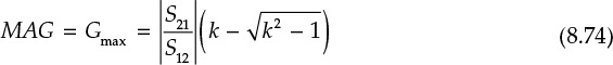
The maximum gain is obtained by substituting ΓSM and ΓLM, given in Equations (8.72) and (8.73), into the transducer power gain, but the calculation is a fairly complicated process and reference 1 at the end of this chapter can be consulted for details. The gain thus obtained is known as the maximum available gain (MAG), Gmax and is expressed in Equation (8.74).
In the case of instability, k < 1, meaningful gain can be derived up to the boundary of the stability condition. Thus, substituting k = 1 into Equation (8.74), the maximum meaningful gain is derived while maintaining stability. This is also known as the maximum stable gain (MSG) and is expressed as
Using the previous S-parameters in Example 8.2, plot the MSG, the MAG, and |S21|2 for FHX35LG/LP in the 1 GHz–20 GHz band. Also, find ΓSM and ΓLM at 12 GHz.
Solution
Enter the following equation in the display window to obtain the MSG and the MAG.
![]() MaxG=max_gain(S)
MaxG=max_gain(S)
Measurement Expression 8E.3 Equation for MSG and MAG
The function max_gain(S) returns MSG for k < 1 and returns the MAG for k > 1. Using the values of k that depend on frequency, it is possible to know whether max_gain(•) represents the MAG or the MSG. Thus, by simultaneously plotting k values together, the max_gain(•) values can be distinguished. The plot is shown in Figure 8E.4. As can be seen from the plot, above 12 GHz, the max_gain plot represents the MAG, while below 12 GHz, it represents the MSG. |S21|2 is also plotted for frequency. By comparing the MAG with |S21|2, the gain improvement by simultaneous conjugate matching can be found.
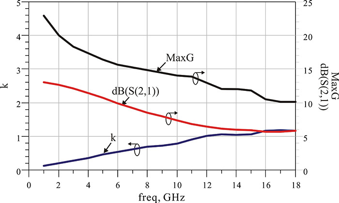
Now we can find ΓSM and ΓLM at a frequency of 12 GHz where the selected device is stable. The ADS functions sm_gamma1(S) and sm_gamma2(S) are used to find ΓSM and ΓLM. The function sm_gamma1(S) gives ΓSM in Equation (8.72), while the function sm_gamma2(S) gives ΓLM in Equation (8.73). In addition, these two functions give 0 when k < 1, and they give the correct values only when k > 1. The function find_index(•) is added to find the corresponding index number to the frequency 12 GHz.
![]() m=find_index(freq, 12G)
m=find_index(freq, 12G)
![]() g1=sm_gamma1(S[m])
g1=sm_gamma1(S[m])
![]() g2=sm_gamma2(S[m])
g2=sm_gamma2(S[m])
Measurement Expression 8E.4 Equations for obtaining the conjugate matching points
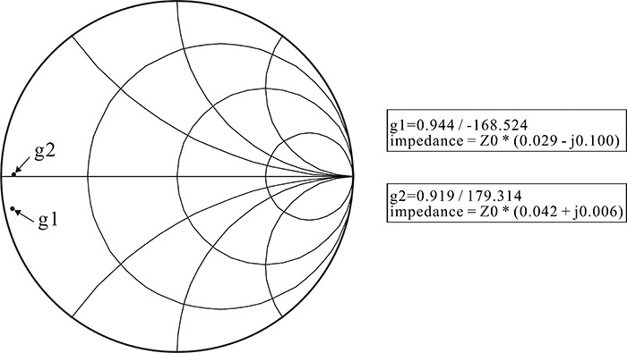
Figure 8E.5 shows g1 and g2 in Measurement Expression 8E.4. The conjugate matching reflection coefficients ΓSM and ΓLM at 12 GHz are read as
ΓSM = 0.944∠ –168.5°
ΓLM = 0.919∠179.3°
8.4 Gain and Noise Circles
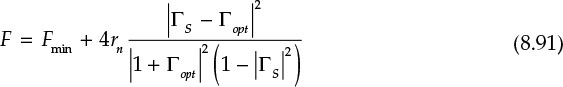
The previously explained ΓSM and ΓLM for the conjugate matching of source and load reflection will yield a maximum gain. However, from a design perspective, other aspects of performance must also be considered, and the source and load reflection coefficients are often set to values other than ΓSM and ΓLM, which can result in decreased gain. We will consider two cases; one when the source reflection coefficient cannot be selected as ΓSM and the other when the load reflection coefficient cannot be selected as ΓLM. In these two cases, the remaining reflection coefficient is usually set to meet the conjugate matching condition. We often need to estimate the subsequent decrease in gain for the two cases. In this section, we will examine constant gain circles as well as constant noise-figure circles.
8.4.1 Gain Circles
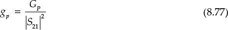
The previously determined power gain in Equation (8.33) can be expressed as Equation (8.34)
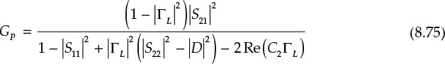
where C2 is defined in Equation (8.76).
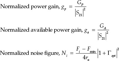
In addition, for ease of mathematical computation, a normalized gain parameter gp is defined as in Equation (8.77).
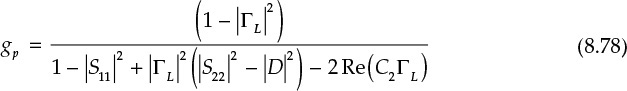
The locus of ΓL giving the same power gain implies that gp is a constant. For a constant gp, Equation (8.75) can be rewritten as Equation (8.78).
With the following definitions expressed in Equations (8.79) and (8.80),
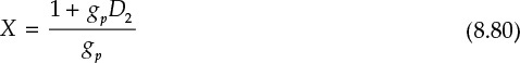
Equation (8.78) can be rewritten as
Then, rewriting Equation (8.81), we obtain
Using Equation (8.82), we can then obtain Equation (8.83) for a circle.
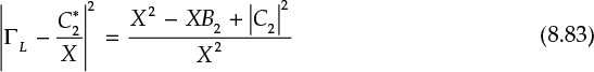
Therefore, the center Cp and radius rp of the circle giving the same power gain are expressed in Equations (8.84) and (8.85).
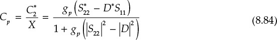
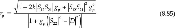
The circle thus obtained is called a power gain circle.
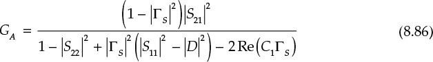
In addition, when ΓL is changed to ΓS and the subscripts 1 and 2 are interchanged in Equation (8.75), it becomes the equation for the available power gain expressed in Equations (8.86) and (8.87).
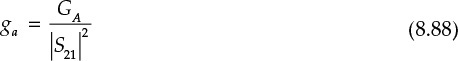
Similarly, to obtain the locus of ΓS with the same available power gain, the following normalized gain is defined in Equation (8.88).
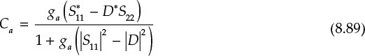
Interchanging the subscripts 1 and 2 in Equations (8.84) and (8.85) will yield the radius ra and center Ca for the available gain circle expressed in Equation (8.89).
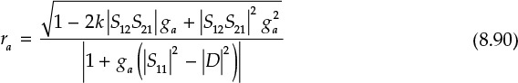
The circles thus obtained are called available gain circles and they have the same available power gain.
8.4.2 Noise Circles
The noise figure obtained in Chapter 4 in terms of the noise parameters depends only on the source reflection coefficient ΓS that is expressed in Equation (8.91).
To obtain the locus of ΓS having the same noise figure, a new noise figure is defined for computational simplicity, as shown in Equation (8.92).
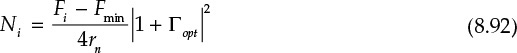
The noise-figure equation can then be written as Equation (8.93).
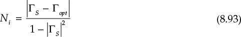
Expanding that equation, it can be written as Equation (8.94).
Equation (8.94) can then be rewritten as
Multiplying both sides of Equation (8.95) by 1 + Ni results in Equation (8.96).
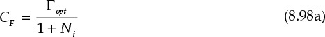
Thus, the locus of ΓS having the same Ni is given in Equation (8.97).
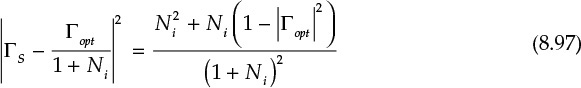
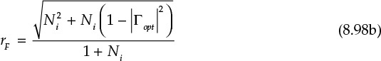
Therefore, the radius rF and center CF of the noise circle are expressed in Equations (8.98a) and (8.98b).
Using the FHX35LG/LP, draw the noise circles and the available power gain circles at 12 GHz.
Solution
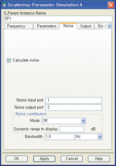
To calculate the noise parameters, open the S-parameter controller, check Calculate noise, and then specify the noise input and output ports as shown in Figure 8E.6. Simulate and then enter the following equations in Measurement Expression 8E.5 in the display window to draw the circles.
![]() ga1=ga_circle(S[m])
ga1=ga_circle(S[m])
![]() ns1=ns_circle({0,1,2,3}+NFmin[m], NFmin[m], Sopt[m], Rn[m]/50, 51)
ns1=ns_circle({0,1,2,3}+NFmin[m], NFmin[m], Sopt[m], Rn[m]/50, 51)
Measurement Expression 8E.5 Equations for drawing the locus of the available power gain circles and the noise circles
The function ns_circle(•) is used for drawing the noise circles given by Equation (8.98), while the function ga_circle(•) is used for drawing the available power gain circles given by Equations (8.89) and (8.90). The function ga_circle(•) draws the available power gain circles lower than the MAG by {1,2,3} dB as the default. The available gain circles plotted by the function ga_circle(•) are shown on the Smith chart in Figure 8E.7. The maximum point of the available power gain circle in the figure is ΓSM.
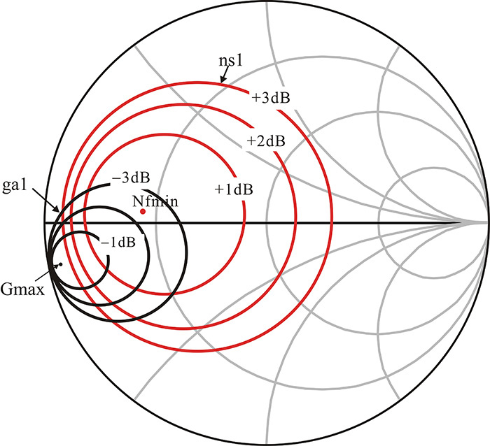
In the variables of the function ns_circle(), {0,1,2,3}+NFmin[m] represents a noise figure lower than the minimum noise figure by {1,2,3} dB. As previously mentioned, m represents the frequency index. To plot the noise circles, the corresponding noise parameters NFmin[m], Sopt[m] and Rn[m]/50 are required. It must be noted that the function ns_circle(•) uses rn, the normalized noise resistance by 50 Ω. The number 51 represents the number of points used for drawing a circle.
8.5 Summary of Gains and Circles
8.5.1 Summary of Gains
Transducer power gain GT is defined as the ratio of the power delivered to the load to the available power from the source, and corresponds to the gain of an amplifier by the usual measurement. In the case of a 50-Ω source and load, ΓS = ΓL = 0, the transducer power gain becomes |S21|2. Thus, |S21|2 is the transducer power gain for a 50-Ω source and load.
First, the available power gain is the gain for a given source reflection coefficient with a conjugate matched load. The available power gain represents the gain degradation due to the specific source reflection coefficient and it is used to evaluate the gain decrease by the source mismatch. Similarly, the power gain is the gain for the selected load with the conjugate matched source, and it represents the gain degradation for selected load reflection coefficient.
Next, the maximum gain appears when the simultaneous conjugate matching at both the input and output of an active device is achieved. The maximum available power gain, MAG, can be obtained if the active device is stable. When it is unstable, the maximum stable gain, MSG, can be obtained at the stability boundary k = 1. The unilateral approximation is applied to estimate the gain. The maximum unilateral gain is an approximate maximum power gain. This clearly shows the extent of the improvement in the transducer power gain |S21|2 by conjugate matching. The passivity or activity of an active device can also be found using the Mason’s gain, which determines whether an active device can amplify or not. The Mason’s gain is the gain that is obtained after the removal of feedback from the output to the input of an active device. The previously described gains are summarized in Table 8.1.
8.5.2 Summary of Circles
The previously derived center and radius for drawing circles on the Smith chart are summarized in Table 8.2. The available power gain circle is the locus of the source reflection coefficient ΓS yielding the same available power gain. Note that the load is assumed to be conjugate matched to the output reflection coefficient Γout given by ΓS. Conversely, the power gain circle is the locus of the load reflection coefficient ΓL yielding the same power gain. In plotting the circles, it is assumed that the source reflection coefficient ΓS is conjugate matched to the input reflection coefficient Γin given by ΓL. The power gain circle shows a gain degradation for a selected load reflection coefficient. Together with the available power gain circles, the power gain circles are commonly used to evaluate gain degradation from the MAG for the selected load or source reflection coefficients in the course of design. Noise circles are used to evaluate the degradation of the noise figure when the source reflection coefficient is not selected for the minimum noise figure, and they are commonly used together with the available gain circles mentioned previously in low-noise amplifier design.
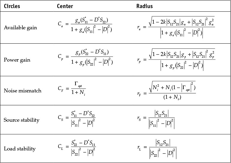
The stability circles help us to determine whether negative resistance appears at the input or output for the selected load or source reflection coefficients, and to know whether or not there is the possibility of oscillation. Accordingly, we are able to identify the region of stability where the load or source reflection coefficients do not induce negative resistance at the input or output. Source stability circles determine whether or not the selected source reflection coefficient is in the region of stability, while the load stability circles determine whether or not the selected load reflection coefficient is in the region of stability.
8.6 Design Example
A low-noise amplifier is an amplifier that has a low noise figure and it is usually located at the front end of a receiver. According to the Frii’s formula, the overall noise figure not only depends on the noise figure of the front-end amplifier, but is also related to the noise figure of subsequent stages. Thus, the overall noise figure depends on both the noise figure and gain of the low-noise amplifier. Because of these facts, the design of the low-noise amplifier can be viewed as a trade-off between the noise figure and the gain. The design involves a process of 1) the appropriate active device selection, 2) the selection of optimal source and load impedances, 3) a design of input and output matching circuits, 4) the addition of DC bias circuits to the matching circuits, and 5) the determination of stability. The selected active device is sometimes unstable at the design frequency. In this case, stabilization is achieved through feedback or by adding small losses to the selected active device. Reference 1 at the end of this chapter provides details of the stabilization method. In addition, considerable attention to the last step of the stability check is recommended since a designed low-noise amplifier often oscillates at frequencies other than the design frequency. This section explains low-noise amplifier design using ADS and is based on the theories previously developed in this book.
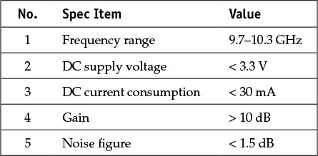
8.6.1 Design Goal
This section presents the design goal of a single-stage low-noise amplifier. As an example, the design specifications for the low-noise amplifier operating in the X-band (8–12 GHz frequency band) are selected, as shown in Table 8.3. The appropriate active device that can satisfy the design specifications must then be selected. It is important that an active device has a minimum noise figure, Fmin, lower than the design goal at the design frequency. Also, the selected active device should have a maximum gain, MAG, greater than the desired gain. An appropriate active device satisfying the design goal may not be available. In that case, the gain can be increased to meet the design goal by cascading a number of stages. Therefore, the key parameter is the noise figure. The active device ATF-36077 is selected to meet the required gain and noise figure and the S-parameters of this device are provided in ADS.
8.6.2 Active Device Model
The active device models can be categorized as a large-signal model and a measured S-parameter data model at a given DC bias, and they can be used in the low-noise amplifier design. The large-signal model of a chip-type active device generally shows a good agreement; however, the S-parameters generated using the large-signal model of a packaged active device at a given DC bias do not generally show a good agreement with the measured S-parameters due to the inaccuracy of the large-signal model. As explained in Chapter 5, the large-signal model of a packaged active device generally does not show sufficient accuracy due to the complexity of the equivalent circuit. Thus, the design of a low-noise amplifier using a packaged device is generally carried out using the measured S-parameter data model. The data models are sometimes already available in the ADS library; otherwise, a user needs to construct the specific data model using given measured data.
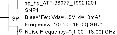
Figure 8.21 shows the S-parameter data model of the ATF-36077 provided in ADS. The model has S-parameter values for 0.5 GHz to 18 GHz at Vds = 1.5 V and Id = 20 mA. No separate DC bias circuit is required to operate the data model and it can be simulated just for the RF signal. In the case of the design that uses a large-signal model, the S-parameters at a given DC bias should be computed by first using the large-signal model, and a similar design can then be carried out using the computed S-parameters following the design shown below.
8.6.3 Device Performance
Figure 8.22 shows an S-parameter simulation set up for determining the stability and maximum gain (MSG or MAG) as well as the minimum noise figure with respect to frequency. In the previous Examples, the determination of the MAG and stability was done in the display window using the built-in measurement expressions. It is also possible to do this in the schematic window, as shown in Figure 8.22. After the simulation, the MAG and stability factor are directly available as variables MaxGain1 and StabFact1 in the dataset.
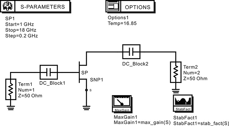
Figure 8.22 Determination of the gain and stability of the ATF-36077. The components MaxGain and StabFact directly yield the MAG and the stability factor in the dataset after the simulation.
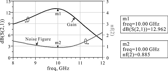
The simulated stability factor, MAG, and the minimum noise figure are shown in Figure 8.23. From Figure 8.23, k is greater than 1 above 16 GHz but k is less than 1 in the design frequency band. The MaxGain1 corresponding to MAG or MSG shows a gain above 15 dB at the design frequency of 10 GHz, as shown in Figure 8.23. Note that MaxGain1 in the design frequency band becomes the MSG because k is less than 1. The minimum noise figure, NFmin is constant as 0.3 dB below 6 GHz. This is not a simulation error. The device data itself is 0.3 dB. In the author’s opinion, because a noise figure below 0.3 dB could not be accurately measured, the data are entered as constant 0.3 dB. However, the minimum noise figure is found to be about 0.5 dB at the design frequency of 10 GHz. Thus, the low-noise amplifier that meets the design specifications can be designed using the selected ATF-36077.
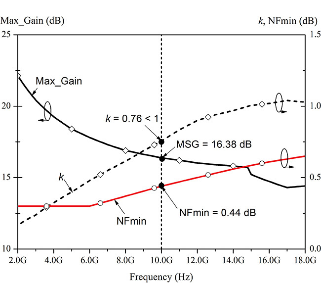
Figure 8.23 Stability factor k, maximum gain, and NFmin with respect to frequency. At 10 GHz, k = 0.76 < 1 and is unstable. The MSG and NFmin at 10 GHz are 16.38 dB and 0.44 dB, respectively.
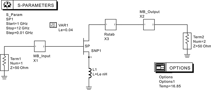
Since the selected device is unstable at the design frequency band, stabilization is necessary to make k greater than 1 at 10 GHz. One way of improving the stability is shown in Figure 8.24. A series feedback inductor Le is connected to the source terminal. To some extent, the inductor added to the source terminal generally increases the stability factor. Figure 8.24 is a circuit setup in which the inductance is swept from 0 to 0.3 nH at a fixed frequency of 10 GHz to evaluate the change in k.
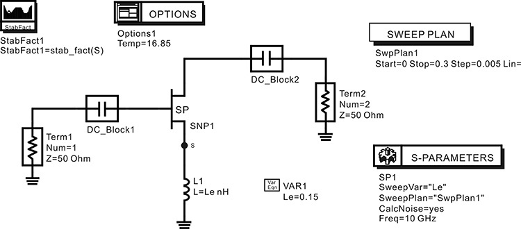
Figure 8.24 Schematic for evaluating the variation of k with the series feedback inductor as a parameter
Figures 8.25(a) and (b) show the simulated stability factor. Figure 8.25(a) shows the stability factor change for Le. From Figure 8.25(a), k has a maximum value of 1.031 at 10 GHz when Le is approximately 0.05 nH, and the stability is thus achieved. Therefore, Le is set to 0.05 nH and k is plotted with respect to frequency as shown in Figure 8.25(b), which shows k greater than 1 at the design frequency. The improvement in the k value is achieved by the addition of Le. However, the bandwidth is narrow and the k value is too close to 1. A slight error in the implementation of Le may cause the active device to be unstable even at 10 GHz and further stabilization would be necessary. There are several other ways to improve the stability of the circuit further. The addition of resistors is one of the methods commonly used (see reference 1 at the end of this chapter). The method of improving k by the addition of a shunt resistor to the drain terminal is used in this book. The reason for the connection to the drain terminal is to minimize the impact of the amplifier on the noise figure.
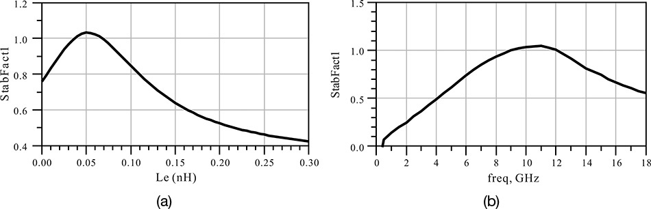
Figure 8.25 (a) Stability factor with respect to the value of Le at 10 GHz and (b) the frequency response of k for Le = 0.05 nH
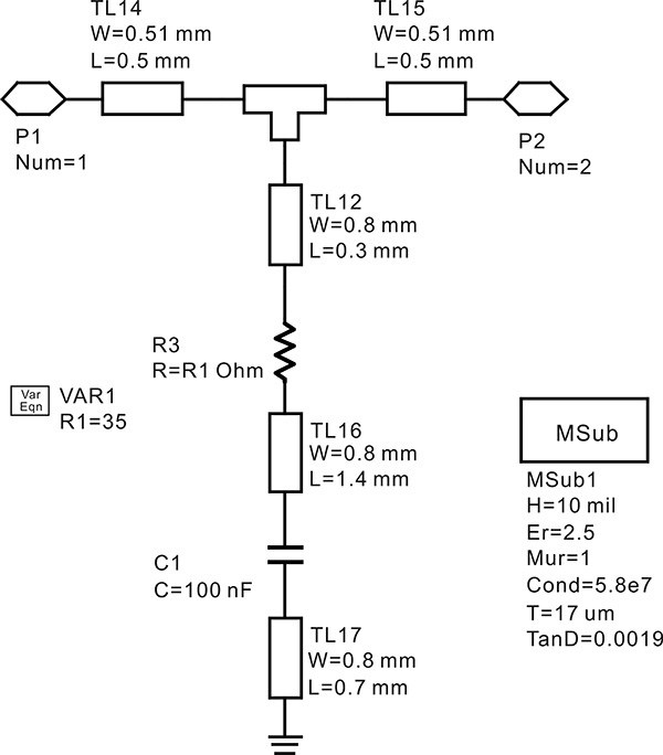
Figure 8.26 shows a shunt stabilizing circuit added to the drain terminal. An R1 = 35 Ω chip resistor (for improving the value of k) is connected in series to a 100 nF DC block capacitor. The microstrip lines represent connecting lines and land patterns for mounting the chip resistor and DC block capacitor. The shunt stabilizing circuit in Figure 8.26 is configured as a subcircuit that is named R_stab. Thus, the amplifier circuit can be represented by a simple schematic, which avoids the necessity of a complex schematic during the design.
The R_stab subcircuit is added to the stability evaluation circuit in Figure 8.24 and a parameter-swept S-parameter simulation for the resistor value R1 in Figure 8.26 is performed to determine the change in k. The value of R1 is swept from 0 to 50 Ω. Figure 8.27(a) shows the k for R1. The value of resistor R1 is selected as 36 Ω. For the value of 36 Ω, Figure 8.27(b) shows the plot of the stability factor for a frequency range of 1–18 GHz. The stability factor k is found to be greater than 1 for wider frequency range. However, the gain slightly decreases due to the resistor added for stabilization, and the effect is slightly compensated by modifying Le = 0.04 nH.
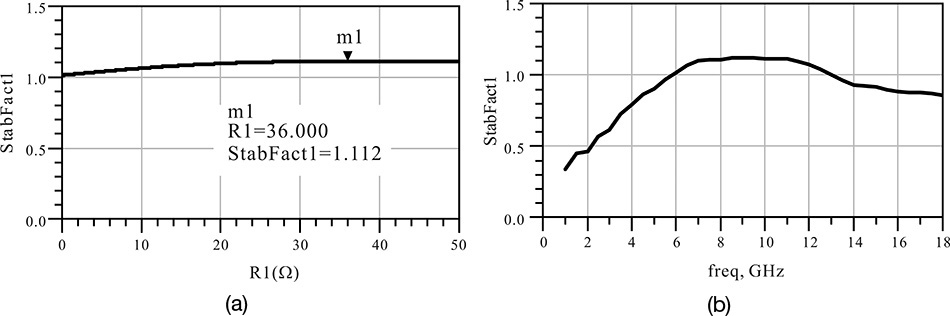
Figure 8.27 The change of k due to the added R_stab subcircuit: (a) the stability factor with respect to resistance R1 at 10 GHz; (b) frequency response of k when the resistance R1 is 36 Ω
8.6.4 Selection of Source and Load Impedances
In this section, we will examine the selection of the source and load impedances to satisfy the design goals. Figure 8.28 is a circuit setup in which the feedback inductor Le and the R_stab subcircuit are added to the active device. To plot the available power gain and the noise circles at 10 GHz, we use the Measurement Expressions in the schematic window shown in Figure 8.28. As previously explained, this can also be done in the display window. In Figure 8.28, three available gain circles whose gain reduces by a 1-dB step from the MAG and three noise circles whose noise figure increases by a 0.2-dB step from the minimum noise figure NFmin are specified. After the simulation, the available gain and noise circles are stored as GaCircle1 and NsCircle1 in the dataset, respectively. The available gain and noise circles are shown in Figure 8.29.
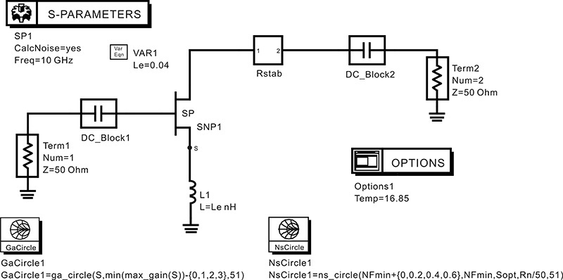
Figure 8.28 Circuit setup for measuring available power gain and noise circles. The available gain circles and noise circles can be directly obtained through the circuit simulation.
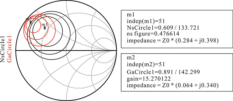
Marker m1 reads the minimum noise figure of 0.47dB, while marker m2 reads the maximum available gain of 15.27 dB. The gain and noise figure performances depend on the choice of the source reflection coefficient, which must be properly selected in accordance with the design goal. Considering the given specifications of a 10-dB gain and a 1.5-dB noise figure, the source reflection coefficient ΓS is selected as marker m1 that has a minimum noise figure of 0.47 dB. The selected source reflection coefficient in Figure 8.29 will give a noise figure of 0.47 dB and a gain above 13 dB.
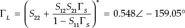
The source reflection coefficient thus selected is ΓS = m1 = 0.609∠133.7°. The corresponding conjugate matching load reflection coefficient is given by
The determined ΓS and ΓL are converted to the impedances, and they are given by
Zsource = (Zin)* = 50*(0.285 + j0.398)
Zload = (Zout)* = 50*(0.301 – j0.169)
To confirm that the selected impedances give the estimated gain and noise figure at the design frequency, the circuit in Figure 8.30 is set up. Since the source and load impedances have the selected impedances, the gain and noise figure should show a gain above 13 dB and a noise figure of 0.47 dB.
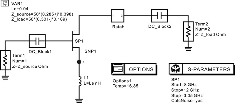
Figure 8.30 Schematic for confirming the selected source and load impedances. The computed impedances are Z_source and Z_load in the variable block named VAR1.
The simulated gain and noise figure are shown in Figure 8.31. As expected, the gain is found to be more than 13 dB and the noise figure is about 0.47 dB at 10 GHz. Thus, the selected impedances yield the gain and noise figure that satisfy the design specifications in the design frequency band. Therefore, the selected source and load impedances are found to be appropriate for the desired low-noise amplifier.
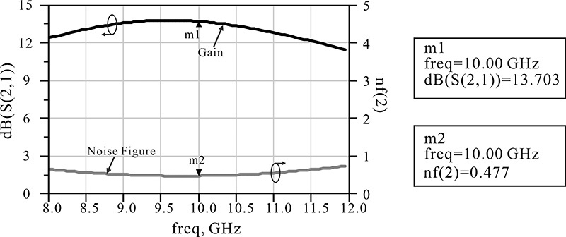
Figure 8.31 Gain and noise figure results for the selected source and load impedances. As expected from Figure 8.29, the gain is above 13 dB and the noise figure is 0.47 dB.
8.6.5 Matching Circuit Design
We found that the desired gain and noise figure can be obtained when the previously selected source and load impedances are connected to the active device. However, actual source and load impedances are 50 Ω, and the matching circuits are necessary to convert the 50-Ω source and load impedances to the previously selected impedances. The lumped-element matching circuits can be designed using the theories previously explained in Chapter 6. However, the optimization is available in ADS and the lumped-element matching circuits can be conveniently designed by the optimization technique. In this section, the lumped-element matching circuits will be primarily designed using the optimization technique. However, for the matching circuits that employ distributed elements such as transmission lines, it is more realistic to implement them on a PCB-like substrate at a frequency of 10 GHz. When microstrip lines are used, impedance matching may be limited by discontinuities, which make it difficult to determine whether or not the matching actually works. Therefore, in this section we will first present the lumped-element matching circuit designs; then, the distributed matching circuits will be designed by replacing the lumped elements with microstrip lines.
8.6.5.1 Lumped-Element Matching Circuits
Figure 8.32 shows a lumped-element input matching circuit. The circuit is set up to determine the values of the lumped-element input matching circuit at 10 GHz using optimization. Port 1 represents the source with a 50-Ω impedance while port 2 represents the input impedance of the active device. The active device’s input impedance is the complex conjugate of the previously selected source impedance. When the maximum power transfer condition is achieved, the impedance seen from port 2 must be the complex conjugate of the port 2 impedance, which is equal to the selected source impedance. Therefore, the matching circuit that gives the desired source-impedance value can be determined.
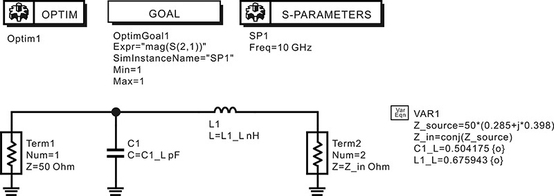
Figure 8.32 Lumped-element input matching circuit setup. Since the impedance seen from port 2 should be the selected Z_source, the impedance of Term2 is set to the conjugate of the Z-source.
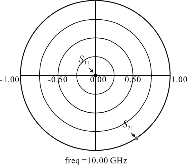
In Figure 8.32, the values of capacitor C1_L and inductor L1_L are optimized for maximum power transfer. The goal is set using |S21| and the maximum power transfer is implemented by setting |S21| = 1. Note that |S21| = 1 is a sufficient condition for conjugate matching. Since the matching circuit consists of lossless elements, the S-parameters satisfy the relation |S11|2 + |S21|2 = 1. Thus, S11 = 0 when |S21|2 = 1. In addition, as the lumped-element matching circuit is a passive circuit, S21 = S12, by invoking the lossless condition it can also be seen that S22 = 0. After the optimization, the values of the lumped-element matching circuit in Figure 8.32 are updated by the optimized values. The value of C1_L is 0.504 pF and that of L1_L is 0.675 nH. Figure 8.33 shows the S-parameters of the lumped-element matching circuit with updated values. It can be seen that |S21| is close to 1 while |S22| is close to 0, which indicates successful impedance matching.
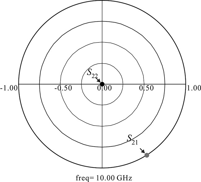
Figure 8.33 Simulation results of the input matching circuit at a frequency of 10 GHz. S11 and S22 are close to 0, while S21 is close to 1. This indicates that the matching is successful.
Similarly, the lumped-element output matching circuit is set up as shown in Figure 8.34. After optimization, the values of the lumped-element output matching circuit are determined as C1_L = 0.478 pF and L1_L = 0.231 nH. The simulated S-parameters for the determined values are shown in Figure 8.35, where |S21| = 1, while |S11| = |S22| = 0 and the successful impedance matching is achieved.

Figure 8.34 Schematic for the lumped-element output matching circuit simulation. Similar to the lumped-element input matching circuit, the impedance of Term1 is set to the conjugate of Z_load.
The lumped-element input and output matching circuits are configured as subcircuits. Using these subcircuits, the low-noise amplifier circuit is configured as shown in Figure 8.36 to confirm the designed matching circuits.
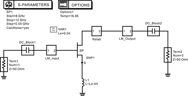
Figure 8.36 The low-noise amplifier circuit composed of the designed lumped-element input and output matching circuits
Figure 8.37 is the simulated gain and noise figure. The gain from Figure 8.37 is found to be more than 13 dB, while the noise figure is below 1.5 dB in the desired frequency band. Due to the frequency-dependent matching circuits, the difference arises as the frequency moves away from the design frequency of 10 GHz.
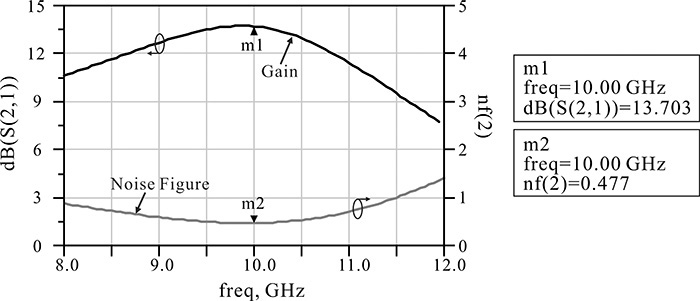
Figure 8.37 Simulation results of the low-noise amplifier composed of lumped-element input and output matching circuits. The gain and the noise figure have almost same values as those in the impedance confirmation.
8.6.5.2 Transmission-Line Matching Circuits
The lumped-element matching circuit discussed in the previous section is intuitive and provides numerous options for design. However, excepting an MMIC, it is generally difficult to implement on a PCB. On the other hand, a matching circuit that uses transmission lines is easy to implement on a PCB-like substrate at high frequency. We will first present the approximate transformation of the previously designed lumped-element matching circuits into the transmission-line matching circuits, and then we will examine a matching circuit design that uses transmission lines.
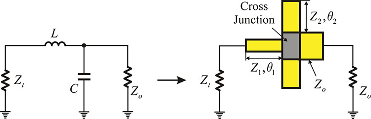
The approximate transformation can be done by replacing the lumped elements with transmission lines. Figure 8.38 shows the transmission-line circuit that can replace the designed lumped-element matching circuit. The transmission line with characteristic impedance Z1 and length θ1 can act as a series inductor, while the two parallel-connected open transmission-line stubs having characteristic impedance Z2 and length θ2 can act as the shunt capacitor. The values of Z1, θ1, Z2, and θ2 can be approximately determined using Equations (8.99a) and (8.99b).
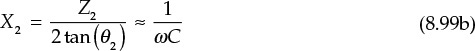
It is worth noting that because the variables in Equation (8.99a) are Z1 and θ1, there are two degrees of freedom in implementing the value of an inductor. The higher Z1 is, the closer it can be implemented as a series inductor. However, considering that the packaged active device is mounted and soldered on top of the inductor transmission line, there should be no problem soldering the active device. Thus, the inductor transmission line has a width wider than that of the active device’s terminal. In addition, the two degrees of freedom are also true for Equation (8.99b), and the lower Z2 is, the closer to a capacitor it will be. However, because increasing the transmission line’s width shortens its length, the implemented transmission-line circuit is close to two cascaded transmission lines with step-discontinuity rather than a cross-junction connection. To avoid this, the lengths of the transmission lines connected at the cross-junction are made greater than their widths.
In addition, when an external circuit is connected directly to the matching circuit, the field of the cross-junction shown in Figure 8.38 may be affected, especially when a coaxial connector is directly connected to the matching circuit. To prevent this, the transmission line with the same value of characteristic impedance Zo is inserted. The output transmission line has no function when viewed from the load side. In addition, the length must be sufficiently long to adequately attenuate the higher-order modes arising in the cross-junction.
Figure 8.39 shows a schematic to determine through optimization the input matching circuit composed of microstrip lines. As previously explained, the microstrip line provides two degrees of freedom, such as the width and length. Of these two, the width is fixed as previously described. The matching circuit is configured by simply changing the length. The width of the transmission line for the shunt capacitor is set slightly wider than the width of a 50-Ω line as W_C = 1.0 mm, while the width of the transmission line for the series inductor is set slightly smaller than the width of a 50-Ω line as W_L = 0.5 mm. With the widths thus fixed, the lengths of the two transmission lines, l_L and l_C are adjusted in a way similar to that of the lumped-element matching circuit until maximum power is delivered. The optimized dimensions are also shown in Figure 8.39.
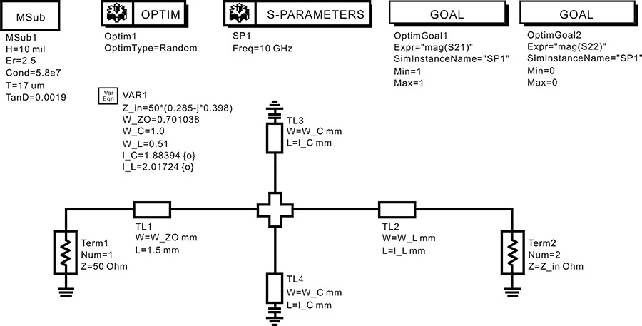
Figure 8.39 Input matching circuit employing microstrip lines. The variable W_ZO represents the 50-Ω width of the microstrip line. W_C and W_L represent the widths of the open-stub and series matching line, respectively. The widths of microstrip lines are fixed and only the lengths are optimized for conjugate matching.
The optimized S-parameters are shown in Figure 8.40, where |S21| = 1 while |S22| = 0, and the successful impedance matching is achieved. Thus, the microstrip-line matching circuit with the optimized dimensions can be used in place of the lumped-element input matching circuit. Similarly, the microstrip-line output matching circuit is set up as shown in Figure 8.41. The length of the microstrip lines l_L and l_C are optimized for the maximum power transfer. The impedance of port 1 is the complex conjugate of the load impedance, while the impedance of port 2 is 50 Ω.
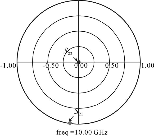
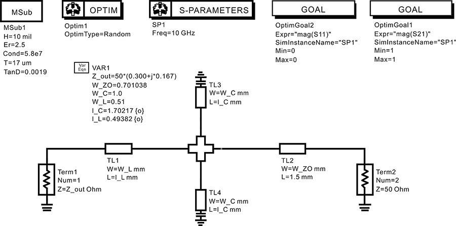
Figure 8.41 Output matching circuit employing microstrip lines. The widths are similarly defined and only the lengths are optimized for conjugate matching.
The S-parameters for the optimized dimensions are shown in Figure 8.42. From the results, |S21| is approximately 1 while |S11| and |S22| are approximately 0, which indicates successful matching. Thus, the microstrip-line matching circuit with the optimized dimensions can be used in place of the lumped-element output matching circuit.
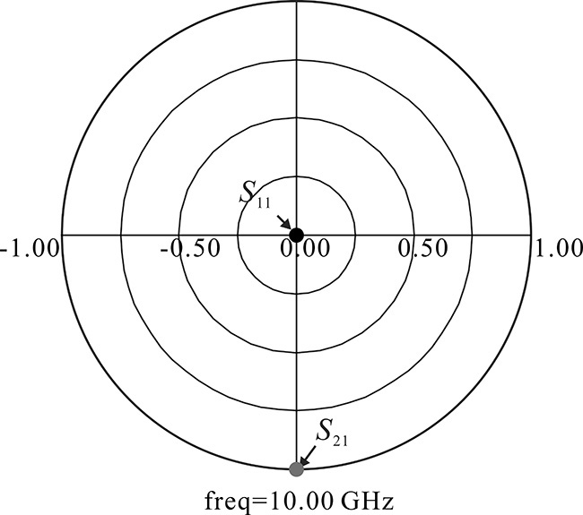
Figure 8.42 Optimization results of microstrip-line output matching circuit at a frequency of 10 GHz
Figure 8.43 shows the simulation results for the low-noise amplifier with the microstrip-line input and output matching circuits. It can be seen that the gain of 13.6 dB and the noise figure of 0.54 dB have been achieved. The values of the gain and the noise figure are close to those that result from using the lumped-element matching circuits. However, the gain is found to be reduced by about 0.1 dB and the noise figure increases by 0.07 dB. This is caused by the losses of the input and output microstrip-line matching circuits.
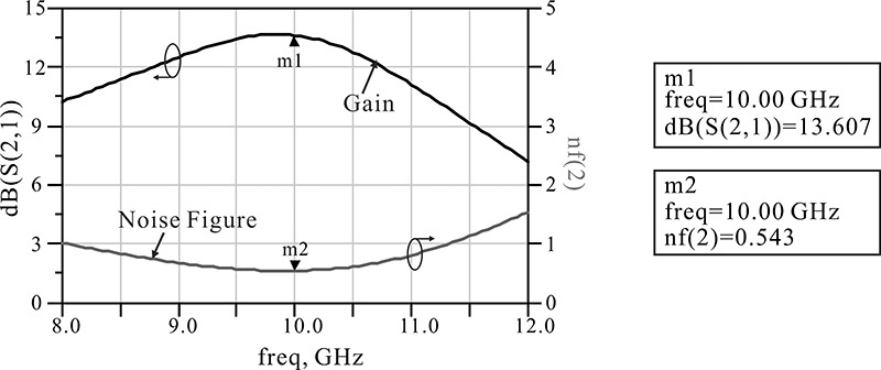
Figure 8.43 Simulation results of the low-noise amplifier composed of microstrip-line matching circuits. The gain is reduced by about 0.1 dB and the noise figure increases by 0.07 dB compared with the gain and the noise figure of the amplifier using the lumped-element matching circuits.
8.6.6 DC Supply Circuit
For the designed low-noise amplifier, an appropriate DC voltage must be applied to the active device through DC supply circuits. These supply circuits must have as minimal an effect on the designed RF matching circuits as possible. Generally, the DC supply circuits will have effects on the matching circuits, and those circuits will have to be redesigned to take into consideration the effects of the DC supply circuits. In this section, we will present a matching circuit design that includes DC supply circuits.
A DC block and an RFC are usually required for DC biasing. Taking into consideration the parasitic inductance discussed in Chapter 2, it is difficult to use chip capacitors as a DC block in the current design’s frequency band. Therefore, the coupled lines shown in Figure 8.44 are usually used as a DC block. However, the spacing between the coupled lines generally tends to be too narrow to be fabricated. In addition, the bandwidth of the coupled-line DC block can also be too narrow. As a result, the values of the previously determined matching circuits can sometimes change significantly due to the coupled-line DC block. Although the redesign of the matching circuits due to the inclusion of the coupled-line DC block is similar to the previous design of the matching circuit, the discussion of the coupled-line DC block will not be covered here.
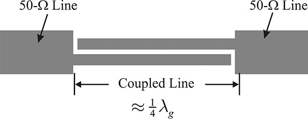
Recently, a high-frequency chip DC block capacitor has been developed and widely commercialized. The advantage of this capacitor is that it generally does not cause any significant changes to the designed matching circuit compared with the coupled-line DC block shown in Figure 8.44. In this section, we will illustrate a process to redesign the matching circuits, including the chip DC block capacitor. ATC’s 1-pF chip DC block capacitor is used as a DC block capacitor.1 The S-parameters of the chip DC block capacitor are provided by the manufacturer and are shown in Figure 8.45, where the 1-pF chip DC block capacitor operates as a DC block from 5 GHz to 26.5 GHz. Using the S-parameters of the chip DC block capacitor that are provided, the chip DC block capacitor can be configured using the S2P data item of ADS. Refer to the datasheet for more details on its frequency characteristics.
1. American Technical Ceramics Corporation, ATC 500S Series BMC Broadband Microwave Millimeter-Wave 0603 NPO SMT Capacitors, available at www.atceramics.com.
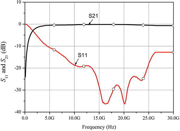
Figure 8.46 shows the redesigned input matching circuit. The chip DC block capacitor is configured as a data item, and the RFC is composed of a quarter-wavelength microstrip line (see Chapter 3) and a radial stub. The dimensions of the radial stub MRSTUB are determined through a separate simulation. The parameters Wi and Angle are fixed, and the length is determined to yield its input impedance 0. The DC gate voltage is applied to the DC bias point shown in Figure 8.46. The radial open stub and DC block capacitor have effects on the designed input matching circuit but they are not significant. Thus, it is necessary to carry out a new optimization. The goals are similar to the previous optimization. The microstrip line lengths l_C and l_L are selected as the optimizing parameters of the input matching circuit, as in the case of the previous optimization process. The other variables such as the line width and length of the RF choke, except length l_C and l_L, are set to be constant and the optimization is carried out. The optimized S-parameters are shown in Figure 8.47. As in the previous optimization, S11 and S22 are both 0, while |S21| is close to 1, indicating successful matching. Note that S21 is slightly less than 1 due to the loss of the microstrip lines and the DC block capacitor.
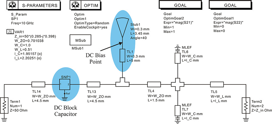
Figure 8.46 Input matching circuit that includes the DC supply circuit. The S-parameter data component is employed for the DC block capacitor. The parameters of the radial stub, Stub1, and choke line, TL1, are separately simulated and fixed. The DC bias point represents the point at which the DC voltage is supplied.
Figure 8.47 Optimization results for the input matching circuit that includes the DC supply circuit. S11 is not shown but it is as close to 0 as S22. Note that S21 has some loss although S11 and S22 are matched. This is due to the loss of the microstrip lines and the DC block capacitor.
Similarly, the output matching circuits are set up as shown in Figure 8.48. The DC block is configured using the data item and the same RFC as in the input matching circuit. The DC drain voltage is supplied at the DC bias point shown in Figure 8.48. The simulation results are shown in Figure 8.49. Similar to the input matching circuit, S11 and S22 are both 0, while |S21| is 1, indicating successful matching.

Figure 8.48 Output matching circuit that includes the DC supply circuit. The circuit is similar to the input microstrip matching circuit.
Figure 8.49 Optimization results for the microstrip output matching circuit that includes the DC supply circuit
Figure 8.50 shows the gain and noise figure of the low-noise amplifier with the determined input and output matching circuits that include the DC supply circuits. The gain at 10 GHz is about 13.7 dB, which is about 0.1 dB less than that of the previous low-noise amplifier. The noise figure increases by approximately 0.3 dB from the previous value of about 0.48 dB. This is believed to be due to the loss of the DC block capacitor.
8.6.7 Stability
The designed low-noise amplifier is obviously stable at the design frequency but the stability at low frequencies is not certain and should be checked. To determine the stability, the source and load stability circles of the active device should first be plotted on the Smith chart with frequency as a parameter. Then, the loci of ΓS and ΓL of the designed matching circuits with frequency as a parameter are plotted together with the corresponding stability circles. The stability can then be determined as to whether or not ΓS and ΓL for each frequency lie in the stable region. Although the process is not difficult, it is very cumbersome.
Alternatively, the stability at low frequency can be checked using the S-parameters of the low-noise amplifier rather than those of the active device. The frequency-dependent stability circles of the low-noise amplifier can be similarly plotted on the Smith chart. In this case, the source and load impedances ΓS and ΓL become the port impedances that result in ΓS = ΓL = 0. Therefore, the stability at low frequency can be checked by determining whether or not the origin of the Smith chart is in the stable region at each frequency. In the latter method, since the source and load stability locus is fixed as ΓS = ΓL = 0, the origin of the Smith chart that repeatedly determines whether or not the origin is in the stable region is visually much easier compared to the former method that checks the stability at the active device plane.
Sometimes, the unstable frequency can be missed because the source and load stability circles are drawn at many discrete frequency samples. The stability of the designed low-noise amplifier means that Γin and Γout for the selected ΓS and ΓL do not show negative resistances. Therefore, |Γin| < 1 and |Γout| < 1 must be satisfied for the selected ΓS and ΓL. In the latter method, Γin = S11 and Γout = S22 and so |S11| < 1 and |S22| < 1 must also be satisfied. Therefore, the determination of low-frequency stability based on the S-parameters of the low-noise amplifier is dependent on:
1. Checking the frequency range in which |S11| > 1 and |S22| > 1.
2. Plotting the stability circles and checking whether their origins are stable or unstable for the frequency range in which |S11|>1 and |S22|>1.
This procedure significantly reduces the work required to check the stability of the designed low-noise amplifier. When the designed matching circuits for the low-noise amplifier are unstable at some low frequencies, the matching circuits should be readjusted until they move out of the unstable region. The circuit shown in Figure 8.51 is set up to determine stability at frequencies other than the design frequency. Note that the matching circuits include the DC bias supply circuits shown in Figures 8.46 and 8.48.
After simulating the S-parameters, |S11| and |S22| are plotted. Fortunately, |S22| < 1 for all frequencies; however, at around 1 GHz, |S11| > 1, as shown in Figure 8.52. Note that |S11| can be greater than 1 because the load ΓL lies in the unstable region. Thus, the load stability circle at 1 GHz is also drawn with S11. The stable region can be determined by using the ADS function l_stab_region(S), which identifies whether or not the inside of the stability circle is stable. The load’s stable regions at 1 GHz are inside the stability circle. This means that the load at the origin of the Smith chart is unstable at 1 GHz. As a result, |S11| is greater than 1 at a frequency of 1 GHz. Therefore, the designed amplifier is unstable at 1 GHz.
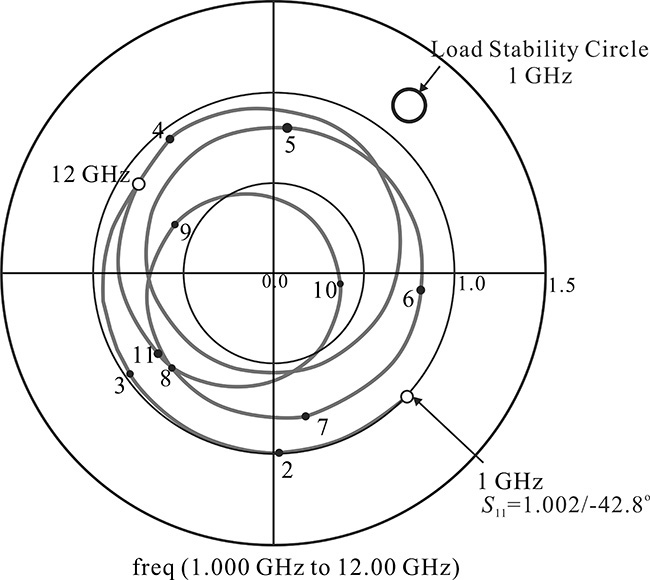
Figure 8.52 Frequency dependence of S11 and load stability circle at 1 GHz. The load is placed at the origin, irrespective of frequency changes. The stable region at 1 GHz is inside the stability circle. As a result, the load is in the unstable region at 1 GHz. The load is stable at other frequencies and the stability circles are not drawn. Also, because |S22| < 1 and the source placed at the origin is stable for all frequencies, they are not drawn.
The reason for the appearance of |S11| > 1 at low frequencies could be attributed to the DC block capacitors inserted in the matching circuits, which open at low frequencies. Therefore, to solve the stability problem, the impedance of the input or output matching circuit seen from the active device is set close to 50 Ω at low frequencies. This looks somewhat like a trial-and-error approach but it is the commonly used method. Usually, the S-parameters of most active devices are measured using 50-Ω reference impedances and the S11 or S22 of active devices is usually less than 1 for most cases; consequently, the devices are stable in these situations. Therefore, for any frequency at which the active device is unstable, setting the impedance seen from the active device into the source or load close to 50 Ω at that frequency will achieve stability. In this sense, the impedance seen from the active device is set close to 50 Ω at low frequencies. Most stabilizing circuits can essentially be regarded as the application of this concept. It is worth noting that the insertion of the low-frequency stabilizing resistors can affect the DC bias voltage or the flow of current, and this must be prevented when inserting the resistors.
In the case of the instability in the designed low-noise amplifier, the modification of the input matching network may be efficient for solving the stability problem. The change in ΓS at 1 GHz will cause changes in the load stability circle’s center and radius at this frequency. Thus, the load at the origin of the Smith chart will be stable. To change the load stability circle’s center and radius, a 50-Ω resistor is inserted in the input matching circuit, as shown in Figure 8.53. The capacitor C1 acts as a bypass capacitor. For the modified input matching circuit, the S-parameters of the amplifier are simulated again with the output matching circuit remaining unchanged. The stability circles S11, and S22 are shown in Figure 8.54.
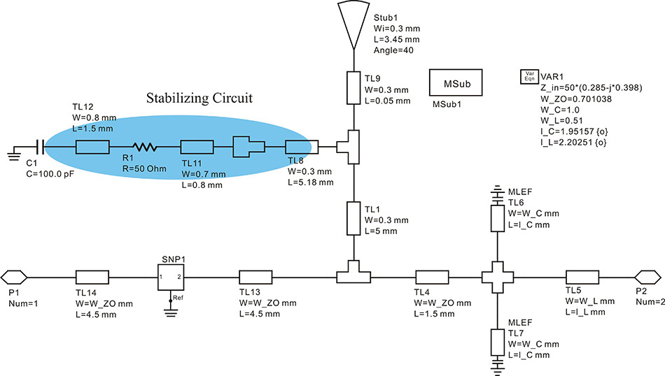
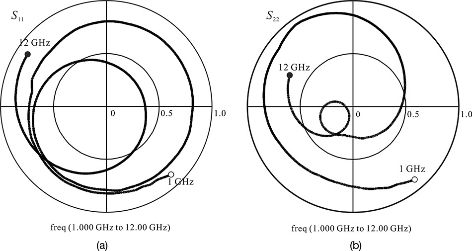
Figure 8.54 S11 and S22 after stabilization. Both S11 and S22 are inside the unit circle and the stabilization is successful.
As can be seen in that figure, both S11 and S22 lie in the unit circle. In conclusion, the low-frequency instability is solved by inserting a low-frequency stabilizing resistor in the DC supply circuit; this must be done carefully so as not to affect the matching circuit at the design frequency. In this way, the instability at low frequencies can be largely eliminated.
8.6.8 Fabrication and Measurements
A layout for the previously designed low-noise amplifier is required in order to fabricate that amplifier. A direct layout for the low-noise amplifier circuit is possible using the autolayout utility in ADS. Note that the layout of the matching circuit generally includes numerous discontinuities that are approximately modeled in the circuit simulation. Consequently, the measured results of the designed low-noise amplifier may differ from the circuit simulation results. A final validation of the amplifier’s layout through EM simulation is necessary for the first pass of the design. In this section, we will begin by describing the implementation of the source inductor at the design frequency. Then, we will discuss the tuning of the matching circuit layouts in Momentum simulation.
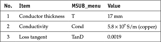
The substrate used for the implementation of the microstrip matching circuits has an inherent dielectric loss as well as a conductor loss due to the finite conductivity of the conductor material. Table 8.4 shows the loss-related parameters of the selected substrate, which is Taconic’s TLX-9;2 the reader may refer to the corresponding datasheet. Note that the substrate losses are not considered in the previously designed low-noise amplifier. The substrate losses can be included in the ADS circuit simulation. It is also possible to include the substrate losses in the settings of the MSUB in the circuit simulation.
2. Taconic Advanced Dielectric Division, TLX, available at www.taconic-add.com/en--index.php.
Careful consideration of the substrate loss is particularly important because the loss degrades the noise figure, especially the substrate loss at the input matching circuit because it degrades the noise figure of the designed low-noise amplifier. Similar optimization techniques can be applied to further refine the values of the matching circuits and take into consideration the substrate loss.
8.6.8.1 Source Inductor
So far, the circuit simulations have been carried out by treating the source inductor as an ideal inductor. However, it is necessary to replace the source inductor by more easily implemented circuit elements such as vias. Since the source inductor is an important element that determines the overall stability of the low-noise amplifier, a careful implementation is required. Figure 8.55 shows the via dimension that is compliant with the manufacturer’s design guidelines. The via dimensions may change depending on those guidelines.
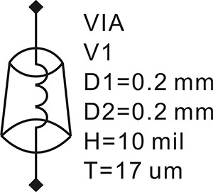
Figure 8.56 shows the distributed inductor circuit for the source inductor. This inductor is implemented using a microstrip line and four vias. The ATF-36077 transistor has two source terminals. Thus, the value of the distributed inductor circuit in Figure 8.56 must have twice the inductance value of the source inductor, so its value is 0.08 nH.
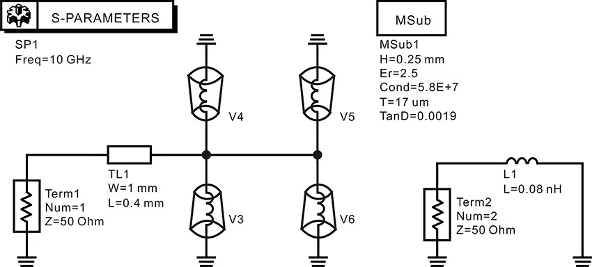
Figure 8.56 Distributed inductor circuit implemented with a microstrip line and four vias. The right-side circuit is the reference inductor circuit.
In Figure 8.56, the reference inductor circuit is shown on the right side and it has an inductance value of 0.08 nH. The reference inductor circuit provides an impedance reference of 0.08 nH. The inductance of a single via is about 0.08 nH. To implement the source inductor, the number of vias is 4, and the inductance of 0.08 nH can be obtained adjusting the microstrip-line length. Sweeping the length of the microstrip line TL1, the appropriate microstrip-line length can be found that makes the impedance of the distributed inductor circuit equal to that of the reference inductor circuit. The value of the microstrip-line length thus obtained through the circuit simulation is shown in Figure 8.56. Then, the layout for the distributed inductor circuit in that figure is generated using the autolayout utility of ADS and modified as shown in Figure 8.57. The layer settings for Momentum simulation are configured by importing the MSUB information in Figure 8.56.
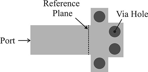
Figure 8.57 Layout implementation of the distributed inductor circuit using a microstrip line and four vias
A slight difference between the Momentum- and circuit-simulated impedances is observed at 10 GHz. In Momentum simulation, by reducing the microstrip-line length that is determined in the circuit simulation, the inductor value of 0.08 nH can be achieved. Figure 8.58 shows the comparison of Momentum- and circuit-simulated impedances with the reference impedance, which is the impedance computed from the reference inductor circuit. It can be seen that the three impedances show good agreement.
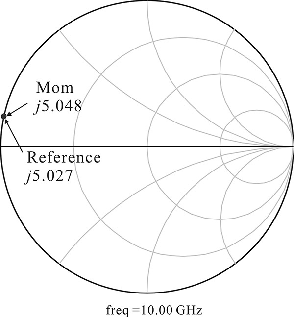
8.6.8.2 Matching Circuits
The matching circuit configurations are the same as the previously designed matching circuit configurations. As a result, the lengths of the matching circuits are slightly modified, but these matching circuits are still not accurate even though the substrate parameters are included in the circuit simulation. Since the approximate models for discontinuities such as T, cross junctions, and so on are used in the circuit simulation, the accurate matching circuits cannot be obtained using circuit simulation alone; thus, they should be verified using Momentum simulation.
The Momentum simulation of the whole matching circuit is still difficult to perform due to its limitations. In particular, Momentum cannot handle the DC block that has an unknown three-dimensional structure. Thus, the DC block and the load-side 50-Ω microstrip line are removed and the layout is prepared for the Momentum simulation. The input matching circuit layout for Momentum simulation is shown in Figure 8.59. Figure 8.60 compares the Momentum-simulated impedances to the circuit-simulated impedances. Here, the circuit-simulated impedance is computed using the circuit that corresponds to the input matching circuit layout in Figure 8.59. Figure 8.60(a) shows the comparison of the two source impedances seen from the active device. Similarly, the output matching circuit layout is prepared and Momentum simulated. Figure 8.60(b) shows the comparison of the load impedances seen from the active device.
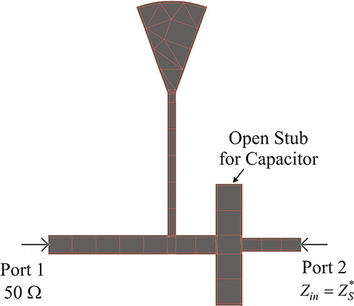
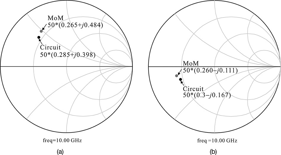
Figure 8.60 Circuit simulation results compared with Momentum simulation results for (a) input and (b) output matching circuit at frequency 10 GHz. They show some differences.
Due to the approximate models for discontinuities in the circuit simulation, the Momentum-simulated impedances are slightly different from the circuit-simulated impedances. Figure 8.61 shows the comparison of the two impedances for the input and output matching circuits after the length adjustments. They are found to show good agreements. The Momentum-simulated impedance is tuned by adjusting the lengths of both the inductor line and the open stub in the matching circuit. The length reduction by about 0.15 mm of the two open stubs in parallel and the reduction by about 0.12 mm for the input matching circuit make the circuit-simulated and Momentum-simulated input impedances coincide, as shown Figure 8.61(a). Similarly, the length reduction by about 0.07 mm of the two open stubs and the reduction by about 0.08 mm of the inductor line for the output matching circuit make the circuit-simulated and Momentum-simulated output impedances coincide, as shown Figure 8.61(b).
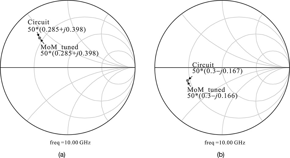
Figure 8.61 Comparison of results for (a) input and (b) output matching circuit after length adjustments are made at 10 GHz. For matching to circuit-simulated impedances, the lengths are adjusted in the Momentum simulation. In the case of the input matching circuit, two open-stub lengths and an inductor-line length are reduced by 0.15 mm and 0.12 mm, respectively. In the case of the output matching circuit, two open-stub lengths and an inductor-line length are reduced by 0.07 mm and 0.08 mm, respectively.
It is necessary to verify whether or not the Momentum-simulated impedances provide adequate performances for the low-noise amplifier. The matching circuits as well as the source inductor obtained from Momentum simulation are represented by the S-parameter data shown in Figure 8.62. Note that the DC block is the same as the circuit simulation and it is also included as a data item. Figure 8.62 shows the circuit setup to confirm the Momentum-simulated results.
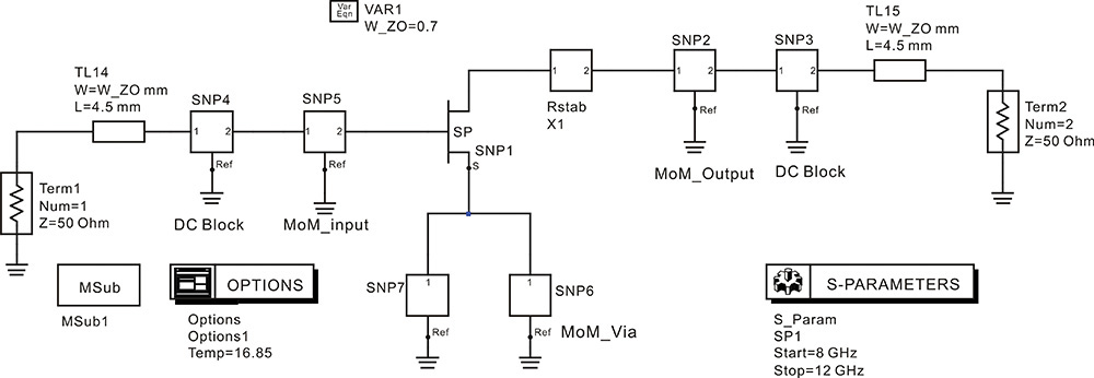
Figure 8.62 Circuit for a low-noise amplifier confirmation using data components. Momentum-simulated results are represented by S-parameter data items.
Figure 8.63 shows the simulated gain and noise figure. The gain is about 13 dB and the noise figure is about 0.9 dB. Comparing the gain and noise figure with those of the circuit-simulation results, it can be seen that the gain has decreased while the noise figure has increased; in particular, the noise figure has increased by 0.2 dB. This is thought to be due to the substrate loss included in the Momentum simulation. However, the gain is found to be more than 12 dB and the noise figure is found to be less than 1.5 dB, which satisfies the design specifications.
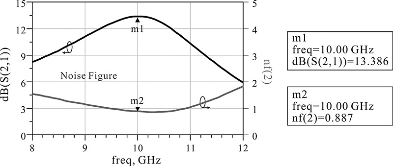
8.6.8.3 Fabrication and Measurement
Figure 8.64 is a photograph of the actual low-noise amplifier fabricated with the settings and simulations described above. The substrate used in the fabrication is Taconic’s 10-mil-thick TLX-9 substrate, which has a dielectric constant of 2.5. ATC’s 1 pF broadband 0603 type 500S was used for the DC block capacitors. The gate bias was applied to the connection point of a 100-pF capacitor and a 51-Ω chip resistor. A 100-pF chip capacitor was also attached in shunt for the drain bias. Next, to prevent the AC noise of the DC power supply, a 3.3 μF tantal capacitor was added to the gate and drain bias.
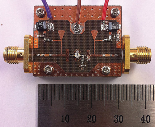
The gate bias voltage was adjusted from the pinch-off voltage until a specified drain current of 10 mA flowed. A gate voltage of VGS = –0.33 V provided the drain current close to 10 mA. The measured drain current was then 10.7 mA. After DC bias adjustment, the noise figure and gain were measured using a noise figure analyzer (NFA). In measuring the noise figure, an attenuator was inserted at the input of the low-noise amplifier. The internal function of the NFA was able to calibrate the inserted attenuator. This was done to reduce the mismatch between the low-noise amplifier and the noise source. After the calibration, the noise figure and gain of the low-noise amplifier was measured.
Figure 8.65 shows the measured and simulated noise figure and gain for the fabricated low-noise amplifier. The measured gain peak shifts downward about 300 MHz and shows the narrower bandwidth compared to the simulated gain. The measured noise figure does not show frequency shift but the noise figure is generally higher than the simulated noise figure. The measured noise figure at 10 GHz is about 1.1 dB, while the simulated noise figure is about 0.89 dB. The noise figure increases by about 0.2 dB. It can be seen that the measured results satisfy the design specifications. However, the measured noise figure and gain show a difference from the simulated noise figure and gain.
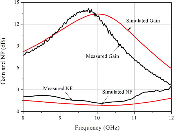
Figure 8.65 Measured gain and noise figure of 10 GHz LNA. The simulated and measured noise figures at 10 GHz are 0.89 dB and 1.1 dB, respectively.
8.6.8.4 Discussion
The reasons for the difference between the measured and simulated gain and noise figure can be a result of the following factors:
1. Substrate parameter variations such as permittivity and thickness.
2. Pattern tolerance in the PCB fabrication.
3. Inaccuracy in the simulation; the S-parameters and noise parameters of the active device may be different from the ADS data.
Factors 1 and 2 cannot explain the shift of the measured gain peak. Since the permittivity change is 2.45–2.55 in the datasheet, the shift of the gain peak is estimated at about
Since Δf is about 300 MHz, Δf cannot be explained using the permittivity change. Also, Δf cannot be explained by the thickness change. Similarly, the pattern tolerance is determined but it cannot explain Δf.
To determine the difference between the measured and simulated gain and noise figure, the S-parameters of the input and output matching circuits are measured. The S-parameters of both the active device with the series feedback inductor and the DC block capacitor are also measured. The measured S-parameters of the input and output matching circuits are close to the simulated S-parameters; however, the S-parameters of the active device show a significant difference compared with the generated S-parameters using the ADS data model. Thus, it can be concluded that the difference in the S-parameters of the active device is the key reason for the difference between the measured and simulated gain and noise figure. This may be caused by differences in the S-parameter measurement environment. In order to verify that the difference of the gains in Figure 8.65 is caused by the difference of the active device’s S-parameters, the gain is computed using the measured S-parameters of the active device and then compared with the measured gain. Figure 8.66 shows the comparison of the computed gain with the measured gain. Although there is still a slight difference, they show good agreement. In conclusion, before creating the design, it is better to measure the S-parameters and noise parameter in advance; the use of measured parameters in the design is also recommended.
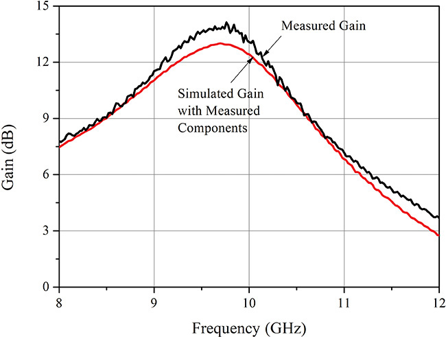
Figure 8.66 Comparison of the measured gain with that computed using the measured parameters. Instead of the ADS data model, the measured S-parameters of the active device are used to compute the gain.
8.7 Summary
• The gain of an amplifier is a function of ΓS, ΓL, and the S-parameters of active devices. Three expressions for gains are derived. The transducer power gain is the ratio of the delivered power to the load to the available power from the source, which represents the conventionally measured gain. The available power gain and power gain are derived for the purposes of the design. The available power gain represents the gain degradation by source mismatch, while the power gain represents the gain degradation by load mismatch.
• A stability check is required to prevent the designed amplifier from becoming an oscillator. A source stability circle is the locus of ΓS, which yields |Γout| = 1. The load stability is the locus of ΓL, which yields |Γin| = 1. Using the stability circles, the stable regions of ΓS and ΓL can be found.
• Stability is determined by using the stability factor k. In the case of unconditional stability, simultaneous conjugate matching is possible.
• Available gain and noise circles provide a convenient way to find the gain and noise figure degradations. Using these circles, we can determine the optimum source and load impedances that satisfy the design objective.
• A low-noise amplifier that satisfies the design objective can be fabricated by following the procedures described below:
1. Select an active device.
2. Perform a stability check at the design frequency. If unstable, stabilize the active device using stabilization circuits.
3. Draw the available gain circles and noise circles.
Determine the optimum source-load impedances.
4. Design input and output matching circuits that give the determined impedances.
5. Add DC bias circuits to the designed matching circuits. Modify the designed matching circuits to compensate for the effects of the DC bias circuit.
6. Perform a stability check at low frequencies. If unstable, modify the matching circuits to make them stable.
7. Perform a layout check with Momentum.
8. Complete fabrication and measurement.
References
1. G. Gonzalez, Microwave Transistor Amplifiers, 2nd ed. Englewood Cliffs, NJ: Prentice Hall, 1997.
2. D. M. Pozar, Microwave Engineering, 2nd ed. New York: John Wiley & Sons, Inc., 1998.
3. G. D. Vendelin, A. M. Pavio, and U. L. Rohde, Microwave Circuit Design Using Linear and Nonlinear Techniques, New York: John Wiley & Sons, Inc., 1990.
Problems
8.1 Referring to Figure 8P.1, determine the Thevenin equivalent circuit based on the reflection coefficient ΓT and bT of the circuit for a 50-Ω measurement reference impedance.
8.2 Prove the transducer power gain in Equation (8.24) using the input reflection coefficient of the active device.
8.3 Available power gain can be directly derived using the Thevenin equivalent circuit at the device output plane rather than using the conjugate matching condition described in Section 8.1.3.2. Derive the available power gain using the Thevenin equivalent circuit at the device output plane shown in Figure 8P.2.
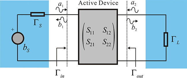
8.4 The power gain is the fraction of the input power delivered to the load. Using this definition, the power gain is derived in the text.
However, power gain can also be thought of as the ratio of the power delivered to the load to the input power when the input is matched for maximum power transfer. Referring to Figure 8P.3, prove the power gain using this definition.
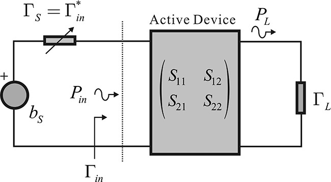
8.5 Solve the ten problems below by using the S-parameters of ATF-35076 in the S-parameter library in ADS shown in Figure 8P.4.
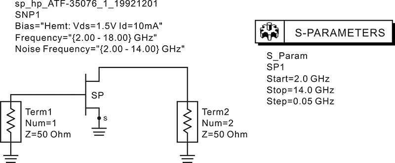
Figure 8P.4 Circuit for Problem 8.5
(1) Plot the stability factor and maximum gain for the frequency range of 2–14 GHz. Find the maximum gain Gmax at 8 GHz and identify this gain as either MSG or MAG.
(2) Find the minimum noise figure Fmin (dB) at 8 GHz. Also, determine if this device is adequate for amplifier design; does it satisfy the noise figure < 1 dB and the gain > 10 dB at 8 GHz?
(3) Figure 8P.5 is a schematic for the stabilization of a transistor using series inductive feedback. Find the value of inductor Ls that yields a maximum stability factor.
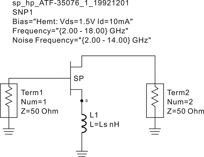
(4) For the selected Ls in Figure 8P.5, find the maximum gain and minimum noise figure at 8 GHz.
(5) Draw the available gain circles degraded by {1, 2, 3} dB from the maximum gain; then draw the noise-figure circles degraded by {0.1, 0.2, 0.3} dB from minimum noise figure.
(6) When source reflection coefficient ΓS is selected to yield the minimum noise-figure point, find the load reflection coefficient ΓL that yields the maximum gain for the selected ΓS. Also, find the corresponding impedances ZS and ZL in real and imaginary formats and find the expected gain Gex and noise figure Fex for the selected impedances.
(7) Plot the frequency response for the frequency range 2–14 GHz with a 0.05-GHz step. Verify the expected gain and noise figure that appear at 8 GHz.
(8) Design the low-pass input and output matching networks with lumped-element inductors and capacitors. Find the values of input and output inductors and capacitors Ci, Li, Co, and Lo.
(9) Using the matching circuits that have the values of inductors and capacitors determined in the preceding step, check the desired gain and noise figure that appear with the frequency response plots for the frequency range of 2–14 GHz with a 0.05-GHz step.
(10) Using DCFEED and DC_Block in ADS, add the bias circuit to the previous amplifier circuit. Find the frequency where the amplifier is unstable using the ADS function for the frequency range 2–14 GHz with a 1-GHz step.