Chapter 15
Unbalanced Outputs
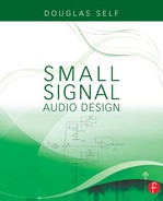
There are only two electrical output terminals for an unbalanced output – signal and ground. However, the unbalanced output stage in Figure 15.1(a) is fitted with a three-pin XLR connector, to emphasize that it is always possible to connect the cold wire in a balanced cable to the ground at the output end and still get all the benefits of common-mode rejection if you have a balanced input. If a two-terminal connector is fitted, the link between the cold wire and ground has to be made inside the connector, as shown in Figure 14.2 in the chapter on line inputs.
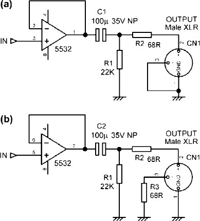
Figure 15.1: Unbalanced outputs. (a) Simple output. (b) Impedance-balanced output for improved CMRR when driving balanced inputs
The output amplifier in Figure 15.1(a) is configured as a unity-gain buffer, though in some cases it will be connected as a series-feedback amplifier to give gain. A non-polarized DC-blocking capacitor C1 is included: 100 μF gives a −3 dB point of 2.6 Hz with one of those notional 600 Ω loads. The op-amp is isolated from the line shunt capacitance by a resistor R2, in the range 47–100 Ω, to ensure HF stability, and this unbalances the hot and cold line impedances. A drain resistor R1 ensures that no charge can be left on the output side of C1; it is placed before R2, so it causes no attenuation. In this case the loss would only be 0.03 dB, but such errors can build up to an irritating level in a large system and it costs nothing to avoid them.
If the cold line is simply grounded as in Figure 15.1(a), then the presence of R2 degrades the CMRR of the interconnection to an uninspiring −43 dB even if the balanced input at the other end of the cable has infinite CMRR in itself and perfectly matched 10 kΩ input impedances.
To fix this problem, Figure 15.1(b) shows what is called an impedance-balanced output. There are now three physical terminals: hot, cold, and ground. The cold terminal is neither an input nor an output, but a resistive termination R3 with the same resistance as the hot terminal output impedance R2. If an unbalanced input is being driven, this cold terminal can be either shorted to ground locally or left open-circuit. The use of the word ‘balanced’ is perhaps unfortunate as when taken together with an XLR output connector it implies a true balanced output with anti-phase outputs, which is not what you are getting. The impedance-balanced approach is not particularly cost-effective, as it requires significant extra money to be spent on an XLR connector. Adding an op-amp inverter to make it a proper balanced output costs little more, especially if there happens to be a spare op-amp half available, and it sounds much better in the specification.
Zero-Impedance Outputs
Both the unbalanced outputs shown in Figure 15.1 have series output resistors to ensure stability when driving cable capacitance. This increases the output impedance and can lead to increased crosstalk in some situations. One such scenario that was fixed by the use of a so-called ‘zero-impedance’ output is described in Chapter 17 in the section on mixer insert points.
Figure 15.2(a) shows how the same technique is applied to an unbalanced output stage with 10 dB of gain. Feedback at audio frequencies is taken from outside isolating resistor R3 via R2, while the HF feedback is taken from inside R3 via C2 so it is not affected by load capacitance and stability is unimpaired. Using a 5532 op-amp, the output impedance is reduced from 68 to 0.24 Ω at 1 kHz – a dramatic reduction that would reduce capacitative crosstalk by 49 dB. Output impedance increases to 2.4 Ω at 10 kHz and 4.8 Ω at 20 kHz as op-amp open-loop gain falls with frequency. The impedance-balancing resistor on the cold pin has been replaced by a link to match the near-zero output impedance at the hot pin.
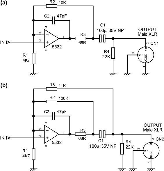
Figure 15.2: (a) Zero-impedance output. (b) Zero-impedance output with NFB around output capacitor
Figure 15.2(b) shows a refinement of this scheme with three feedback paths. In Chapter 2 we saw how electrolytic coupling capacitors can introduce distortion even if the time-constant is long enough to give a flat LF response. In Figure 15.2(b) most of the feedback is now taken from outside C1, via R5, so it can correct capacitor distortion. The DC feedback goes via R2, now much higher in value, and the HF feedback goes through C2 as before to maintain stability with capacitative loads. R2 and R5 in parallel come to 10 kΩ so the gain is the same. Any circuit with separate DC and AC feedback paths must be checked carefully for frequency response irregularities, which may happen well below 10 Hz.
Ground-Canceling Outputs
This technique, also called a ground-compensated output, appeared in the early 1980s in mixing consoles. It allows ground voltages to be canceled out even if the receiving equipment has an unbalanced input; it prevents any possibility of creating a phase error by mis-wiring, and it costs virtually nothing except for the provision of a three-pin output connector.
Ground canceling (GC) separates the wanted signal from the unwanted ground voltage by addition at the output end of the link, rather than by subtraction at the input end. If the receiving equipment ground differs in voltage from the sending ground, then this difference is added to the output signal so that the signal reaching the receiving equipment has the same ground voltage superimposed upon it. Input and ground therefore move together and the ground voltage has no effect, subject to the usual effects of component tolerances. The connecting lead is differently wired from the more common unbalanced-out balanced-in situation, as now the cold line is to be joined to ground at the input or receiving end.
An inverting unity-gain ground-cancel output stage is shown in Figure 15.3(a). The cold pin of the output socket is now an input, and has a unity-gain path summing into the main signal going to the hot output pin to add the ground voltage. This path R3, R4 has a very low input impedance equal to the hot terminal output impedance so if it is used with a balanced input, the line impedances will be balanced, and the combination will still work effectively. The 6 dB of attenuation in the R3–R4 divider is undone by the gain of 2 set by R5, R6. It is unfamiliar to most people to have the cold pin of an output socket as a low impedance input, and its very low input impedance minimizes the problems caused by mis-wiring. Shorting it locally to ground merely converts the output to a standard unbalanced type. On the other hand, if the cold input is left unconnected then there will be a negligible increase in noise due to the very low input resistance of R3.

Figure 15.3: (a) Inverting ground-canceling output. (b) Non-inverting ground-canceling output. (c) A true balanced output
This is the most economical GC output, and is very useful to follow an inverting summing amplifier as it corrects the phase. Obviously the phase inversion is not always convenient, and Figure 15.3(b) shows a non-inverting GC output stage with a gain of 6.6 dB. R5 and R6 set up a gain of 9.9 dB for the amplifier, but the overall gain is reduced by 3.3 dB by attenuator R3, R4. The cold line is now terminated by R7, and any signal coming in via the cold pin is attenuated by R3, R4 and summed at unity gain with the input signal. The stage must be fed from a very low impedance such as an op-amp output to work properly. There is a slight compromise on noise performance here because attenuation is followed by amplification.
Ground-canceling outputs are an economical way of making ground loops innocuous when there is no balanced input, and it is rather surprising they are not more popular; perhaps people find the notion of an input pin on an output connector unsettling. In particular, GC outputs would appear to offer the possibility of a quieter interconnection than the standard balanced interconnection because a relatively noisy balanced input is not required (see Chapter 14). Ground-canceling outputs can also be made zero-impedance using the techniques described earlier.
Figure 15.3(c) shows a balanced output, where the cold terminal carries the same signal as the hot terminal but phase-inverted. This can be arranged simply by using an op-amp stage to invert the normal in-phase output. The resistors R3, R4 around the inverter should be as low in value as possible to minimize Johnson noise, because this stage is working at a noise gain of 2, but bear in mind that R3 is effectively grounded at one end and its loading, as well as the external load, must be driven by the first op-amp. A unity-gain follower is shown for the first amplifier, but this can be any other shunt or series-feedback stage as convenient. The inverting output if not required can be ignored; it must not be grounded, because the inverting op-amp will then spend most of its time clipping in current limiting, probably injecting unpleasant distortion into the grounding system. Both hot and cold outputs must have the same output impedances (R2, R6) to keep the line impedances balanced and the interconnection CMRR maximized.
A balanced output has the advantage that the total signal level on the line is increased by 6 dB, which if correctly handled can improve the signal-to-noise ratio. It is also less likely to crosstalk to other lines even if they are unbalanced, as the currents injected via the stray capacitance from each line will tend to cancel; how well this works depends on the physical layout of the conductors. All balanced outputs give the facility of correcting phase errors by swapping hot and cold outputs. This is, however, a two-edged sword, because it is probably how the phase got wrong in the first place.
There is no need to worry about the exact symmetry of level for the two output signals; ordinary tolerance resistors are fine. Such gain errors only affect the signal-handling capacity of the interconnection by a small amount. This simple form of balanced output is the norm in hi-fi balanced interconnection, but is less common in professional audio, where the quasi-floating output described below gives more flexibility.
Quasi-Floating Outputs
The purely electronic output stage in Figure 15.4(a) emulates a floating transformer winding; if both hot and cold outputs are driving signal lines, then the outputs are balanced, as if a center-tapped output transformer were being used, though clearly the output is not galvanically isolated from ground. If, however, the cold output is grounded, the hot output doubles in amplitude so the total level hot-to-cold is unchanged. This condition is detected by the current-sensing feedback taken from the outside of the 75 Ω resistor R10, and the current driven into the shorted cold output is automatically reduced to a low level that will not cause problems.
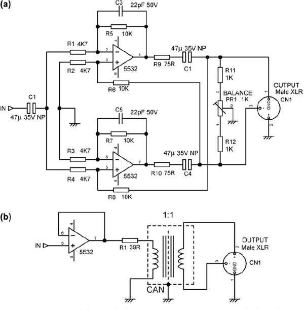
Figure 15.4: (a) Quasi-floating balanced output. (b) Transformer balanced output
Similarly, if the hot output is grounded, the cold output doubles in amplitude and remains out of phase; the total hot–cold signal level is once more unchanged. This system has the advantage that it can give the same level into either a balanced or unbalanced input, given an appropriate connector at the input end; 6 dB of headroom are, however, lost when the output is used in unbalanced mode. It is most useful in recording studios where various bits of equipment may be temporarily connected; it is of less value in a PA system with a fixed equipment line-up.
When an unbalanced output is being driven, the quasi-floating output can be wired to work as a ground-canceling connection, with rejection of ground noise no less effective than the true balanced mode. This requires the cold output to be grounded at the remote (input) end of the cable. Under adverse conditions this might cause HF instability, but in general the approach is sound. If you are using exceptionally long cable, then it is wise to check that all is well.
If the cold output is grounded locally, i.e. at the sending end of the cable, then it works as a simple unbalanced output, with no noise rejection. When a quasi-floating output stage is used unbalanced, the cold leg must be grounded, or common-mode noise will degrade the noise floor by at least 10 dB, and there may be other problems with increased distortion.
Quasi-floating outputs use a rather subtle mixture of positive and negative feedback of current and voltage. This performs the required function quite well, but a serious drawback is that it accentuates the effect of resistor tolerances, and so a preset resistor is normally required to set the outputs for equal amplitude; the usual arrangement is shown in Figure 15.4(a). If it is not correctly adjusted one side of the output will clip before the other and reduce the total output headroom. This is a set-and-forget adjustment unless it becomes necessary to change any of the resistors in the circuit.
Transformer Balanced Outputs
If true galvanic isolation between equipment grounds is required, this can only be achieved with a transformer. The technique is not that common, because of the cost, weight, and performance problems of transformers, but is sometimes found in touring PA systems (for example, in the mic-splitter box on the stage) and broadcast environments where huge RF field strengths are encountered. It is also used for test-gear outputs to prevent ground-loop formation. A basic transformer balanced output is shown in Figure 15.4(b).
Transformers have well-known problems with linearity at low frequencies. This is because the voltage induced into the secondary winding depends on the rate of change of the magnetic field in the core, and so the lower the frequency, the greater the change in magnitude must be for transformer action. The current drawn by the primary winding to establish this field is non-linear, because of the well-known non-linearity of iron cores. If the primary had zero resistance, and was fed from a zero source impedance, as much distorted current as was needed would be drawn and no one would ever know there was a problem. But… there is always some primary resistance, and this alters the primary current drawn so that distortion is introduced into the magnetic field established, and so into the secondary output voltage. Sometimes there is also series resistance such as R1 deliberately inserted into the primary circuit, presumably with the intention of avoiding HF in stability provoked by transformer winding and line capacitances; this makes the LF distortion problem worse, and a better means of isolation is a low-value inductor of say 4 μH in parallel with a low-value damping resistor of around 47 Ω.
The LF distortion can be reduced by applying negative feedback via a tertiary transformer winding. Another cure is to cancel out the transformer primary resistance by an electronically generated negative resistance; comprehensive details on this approach can be found in Bruce Hofer’s patent, which covers the transformer output of the Audio Precision System 1 [1]. DC flowing through the primary winding is also bad for linearity, and if necessary should be stopped by a DC-blocking capacitor.
The output stages described above assume that the load to be driven will not be less than 600 Ω and can be handled by a single 5532 op-amp section. If you want to keep optimal linearity then the lower limit is perhaps 700–800 Ω. There are many reasons to drive lower load resistance, such as headphone outputs, or driving special low-resistance circuitry designed to minimize noise.
Op-amps do exist with a greater load-driving capability – for example, the NJM4556A from JRC is capable of driving 150 Ω, but this device seems to have achieved little market penetration, possibly because its linearity even into light loads is distinctly inferior to that of the 5532. In 2009 none of the usual distributors is carrying it, and it is not clear if it is still in production.
In some circumstances paralleled 5532 stages are the simplest answer. In Figure 15.5 the upper trace shows a single 5532 section attempting to drive 5 Vrms into 220 Ω. The distortion is very high for a 5532, and it is clearly running out of current capability. Adding a second section in parallel with the outputs coupled by 10 Ω resistors, as shown in Figure 1.10 in Chapter 1, drops the THD back to almost nothing. The gains of the paralleled voltage-follower stages are very closely equal, so the small series output resistors can allow for minor gain mismatches and prevent currents passing from op-amp to op-amp.

Figure 15.5: One and two 5532 sections attempting to drive 5 Vrms into 220 Ω
This can be a very simple and cost-effective way to solve the problem of driving medium loads, and it can be extended by connecting more 5532 sections in parallel, apparently without limit. Figure 15.6 shows four parallel 5532 sections driving 100 Ω to 5 Vrms with very little distortion. An array of 12 parallel 5532 sections can drive a 25 Ω load with 5 Vrms very effectively, and I have experimentally driven 8 Ω speakers in the same way, at extremely low distortion. That does, however, require rather a lot of 5532s.

Figure 15.6: Four parallel 5532 sections driving 100 Ω with 5 Vrms. The THD plot is almost identical to that of two 5532 sections driving 220 Ω
As described in Chapter 1, paralleled op-amps not only increase drive capability but also reduce noise and allow a lower effective output impedance when driving capacitative loads.
For loads beyond the capabilities of the two halves of a 5532 in parallel, it may be more economical to adopt a hybrid circuit. (These are ‘hybrid’ circuits in that they combine IC op-amps with discrete transistors; the name does not refer to thick-film construction or anything like that.) The usual procedure is to add a Class-B output stage after the op-amp. A Class-A output stage is perfectly feasible if ultimate quality is required, though the power consumption is naturally much higher.
The arrangement in Figure 15.7(a) is economical and dependable, and I have used it to drive headphones in low-cost mixing consoles. The output stage is the simplest possible version of Class-B, but it really works quite well, though its distortion characteristics, as seen in Figure 15.8, are not comparable with a 5532’s. The output devices are TO-92 small-signal types with high beta, and this is crucial to an acceptable distortion performance; the bias is fixed by D1, D2. Gain is 3.2 times. Inserting extra stages into op-amp feedback loops must be done with care, to avoid adding extra phase-shifts that may cause HF instability; here there are no problems, and no extra stabilizing components are required. The output is AC coupled by C2 so that DC-offset protection is not required, and output resistor R7 takes care of short-circuit protection, and also does something to cater for the different levels of drive required by 600 and 30 Ω headphones; it seems to be generally accepted that headphones do not require a very low output impedance.

Figure 15.7: Two headphone amplifiers that combine a TL072 with a discrete Class-B output stage. (a) The basic version. (b) A superior variant giving greater output and lower distortion
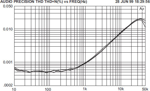
Figure 15.8: THD against load for TL072 with discrete Class-B output stage. No-load, 470R, and 220R loading. Gain 3×, output level 7.75 Vrms (before output series resistor)
The arrangement in Figure 15.7(b) is a deluxe version with lower distortion and greater output into lower impedances. I have deployed it in high-end mixing consoles and in preamplifiers with a headphone output. The gain is higher at 5.7 times, and is provided by U1:A, allowing U1:B to work at unity gain so it has maximal negative feedback for correcting errors in the output stage. Bootstrapping is added to R4, R7 to maintain a more constant current through bias diodes D1, D2. The distortion is reduced to 0.002% at 10 kHz and 0.004% at 20 kHz with 6 Vrms at the amplifier output when driving a 30 Ω load.
Reference
[1] B. Hofer, Low-distortion transformer-coupled circuit, US patent no. 4,614,914 (1986).
Small Signal Audio Design; ISBN: 9780240521770
Copyright © 2010 Elsevier Ltd; All rights of reproduction, in any form, reserved.