
3
Hardware Design Using VHDL
3.1 HARDWARE DESIGN LANGUAGES
As already noted in section 1.2, circuits composed of building blocks can be understood as a special way to realize algorithms in hardware and be specified by means of the algorithmic notation found in programming languages. For the design of digital systems (and for real-time programming) the timing behavior of the execution of operations is important (see section 1.4), in particular, the timing of the events of changing signal levels. For the purpose of defining digital hardware structures, including their timing, hardware design languages (HDL) have emerged that as well as defining the operations to be performed also specify their timing. A common HDL is VHDL, others are Verilog, ELLA [69], and extended versions of standard languages like C, e.g. System C [70], and Handel-C which goes back to [29].
For a long time, hardware designers drew circuit diagrams (‘schematics’) showing the interconnection of components (gates, registers, processors, etc.), using special shapes or annotations to distinguish the different building blocks. This is adequate for showing the structure of a design, and can be supported by using a graphics editor for schematic entry. It does not cover the specification of the timing behavior as a basis of timing simulations and verification. Algorithms are read more easily from a textual representation, and sometimes a hardware description is only given up to the point of specifying its behavior (the timing and the transfer functions of the building blocks) but not the details of the algorithms to be used. A building block might e.g. be described to perform an add operation on 16-bit codes of numbers within a certain processing time without specifying which Boolean algorithm should actually be selected for it. These aspects are taken care of by the hardware design languages.
By now, apart from the level of connecting large standard building blocks on a circuit board, hardware design is mostly done using some HDL. From an HDL description the interconnection network of basic components can automatically be extracted and mapped to the resources of a chip or an FPGA. If the description only specifies the behavior but not the implementation of some of the building blocks, the synthesis of the network of basic components is still possible by using default implementations. The tool chains offered by FPGA vendors include HDL design entry tools for the most common HDLs.
An HDL takes a point of view that differs in some respects from conventional software languages. The statements in a software language are implicitly understood to be executed one-by-one. In contrast, the statements in an HDL describing the operations to be performed and the signals to be output are essentially executed in parallel. They may exhibit data dependencies but they are not bound to the serial execution in the textual order. Second, software programmers use local variables to store intermediate results of a computation. Although storage elements play an important role in digital hardware, intermediate results may be passed directly from the output of a building block to the input of another one. The assignment to a local variable must be understood as naming the output signal of an operation just for the purpose of being able to reference it. Whereas sequential programs may use the same variable to store different values at different times, this makes no sense for naming an output signal. Thus the assignment of a value to a name must be unique. Storage will only be involved if the signal data at the time of a particular event (defined by some change of a control signal) have to be used at a later time. Finally, software programmers use functions and procedures with the understanding of defining sub-routines which may be jumped to. In a higher level language they mainly serve the purpose of gaining more abstraction by referencing a composite action by a short name, and a hierarchical structure due to allowing nested function calls. In a hardware circuit there is no way to jump into or to return from a sub-structure (although a sub-circuit may be applied sequentially for several times). A call must be interpreted in such a way that an individual sub-circuit of the structure defined in the algorithm for the function has to be inserted at the call site. These slight restrictions and changes to the interpretation of software languages provide the abstraction from the working of a sequential machine. Then the same programming language can be used for algorithms that are alternatively realized in software or in hardware (excluding the definitions of their timing behaviors which are mostly needed for a timing simulation to verify the proper operation and existing timing constraints). This would be attractive for digital systems realizing some processing by means of composite hardware circuits and other functions on programmable processors. The most common HDLs, however, have evolved into dedicated ones and include structures that have no meaning to processor software whereas processor software is implemented with dedicated software languages. The algorithmic notation provided in VDHL is used for behavioral descriptions only while the composition of circuits uses an extra notation not applicable to sequential software. We'll come back to the system design in a common language for both hardware and software functions in Chapter 7.
In the sequel, VHDL will be introduced informally as one of the most common HDLs for the purposes of subsequently describing the most common sub-structures of digital systems beyond the level of gates and registers and to provide the basics to enable practical design exercises on FPGA using a standard tool chain. A more comprehensive presentation of VHDL can e.g. be found in [30]. The discussion of VHDL will give us the opportunity to formally describe the timing of the basic circuit elements introduced in Chapter 2 and the timing relationships of events (Chapter 1). We will still use diagrams if only the interconnection structure is considered. VHDL is a special purpose language for describing and designing digital hardware, and for simulating its operation. The only run time environment for VHDL ‘programs’ is the VHDL circuit simulator. VHDL also serves to synthesize circuit structures, but it cannot be used to generate executable code for processors or other control parameters for sequential sub-systems.
3.2 ENTITIES AND SIGNALS
VHDL describes the functional behavior of circuits, their timing, i.e. the events of changing input and output data according to their execution times, and their structure. The language is dedicated to describing idealized digital systems where the signals are binary and make their transitions at well-defined times at zero duration. The transfer of a signal from the output of a sub-circuit to the input of another one also takes zero time. The functional behavior is defined through Boolean functions that may be given as tables, as Boolean expressions or by other algorithms. VHDL is intended to define and simulate digital hardware before it is actually built, and also serves as a formal language from which the information needed to produce the hardware (e.g. the configuration code of an FPGA) is synthesized automatically by a compiler. A VHDL design defines some hardware system as well as the application-specific building blocks for it. All of these become design ‘units’ in the some default VHDL library (usually named WORK). Typically, there is also a design unit containing the main system and supplying it with input signals for testing purposes. Other libraries are used to supply additional design units.
The types of circuit building blocks described in VHDL are called entities. Once an entity has been defined, other definitions may use instances of it which are separate building blocks of the same type. The circuits described in VHDL have input and output signals and internal signals which are set to specific values at specific times. The definition of an entity is divided into a definition of its interface signals and definitions of its behavior or its structure as a composition of other building blocks, or as a mixture of both. An entity may be given both structural and behavioral descriptions. The structural definition of an entity implies a behavior resulting from the behavior of the components used therein. A behavioral description is not automatically checked to be compatible with the behavior of a structural definition. If several competing definitions are given, extra control statements are used to define which one should be used for the purpose of simulation or the extraction of a network of basic components. For the most elementary circuit types that are not composed of sub-circuits, only a behavioral definition can be given. These definitions are usually taken from a standard library.
The signals used in an entity need to be declared as interface or internal signals of some type defining the possible values. Standard signal types are ‘bit’ which is an enumerated data type containing the symbols (not the numbers) ‘0’ and ‘1’, or the type ‘std_logic’ defined in the IEEE library STD_LOGIC_1164 which also allows the symbol ‘Z’ as a value indicating a high impedance state of the signal, and six more values. ‘U’ indicates an uninitialized state, ‘X’ a bus conflict, ‘H’ and ‘L’ are logic levels generated by pull-up or pull-down resistors, ‘W’ an intermediate value, and ‘-’ is a ‘don't care’ value. Signals of the generic types ‘bit_vector’ or ‘std_logic_vector’ take n-tuples as values. The index range used for the tuples needs to be specified as a parameter. It is an expression such as ‘n − 1 downto 0’ or ‘0 to n − 1’ or a similar one denoting an integer interval containing n indices. Bit vector literals are written as strings that may contain the ‘0’ and ‘1’ characters and underline characters for the sake of readability (octal and hexadecimal literals are also supported). “01_00” is a bit vector of size four and can be assigned to signals of this size. VHDL also provides numeric data types, namely the types ‘integer’ and ‘real’ covering the ranges of 32-bit signed binary and single-precision floating point numbers. Bit strings and the values of signals are distinguished from the numbers they might represent. The arithmetic operations are not defined for the ‘bit_vector’ and ‘std_logic_vector’ types, but for numeric types. Other bit field data types can, however, be defined, and it is possible to define (overload) the arithmetic operators for such. The types ‘signed’ and ‘unsigned’ are defined in the IEEE libraries NUMERIC_BIT and NUMERIC_STD as vector types that are signed binary or binary numbers, and the arithmetic operations are defined for these. For the specification and simulation of times VHDL provides the ‘physical’ type ‘time’, the values of which are numeric multiples of one of the units ‘s’,‘ms‘,‘us‘,‘ns‘,‘ps’ or ‘fs’.
The interface part for an entity starts with the keyword ‘entity’ and the name of the circuit type to be defined. The interface signals are specified in a ‘port’ definition and given directional attributes ‘in’, ‘out’, or ‘buffer’ and a signal type. ‘buffer’ is similar to ‘out’ but allows the signal values not just to be assigned but also to be read and used like input signals. The attribute ‘inout’ is used for bi-directional bus signals of a type providing a high-impedance state ‘Z’. Such signals may be driven from several sources. If ‘Z’ is output, but ‘0’ or ‘1’ is output from another (external) source, the signal will assume these latter values (signal resolution).
The structural or behavioral descriptions for the entity are introduced with the keyword ‘architecture’, a name for this architecture, and the reference to the circuit type to be described. It is followed by declarations of the additional internal signals used by this particular definition. They have no directional attributes but just a signal type and can be used like ‘in’ signals but need to be assigned values, too. The actual definition is enclosed between the ‘begin’ and ‘end’ keywords (see Listing 3.1).
The definition of an entity is preceded by a specification of the required additional libraries and the particular packages and definitions to be used therein, e.g.:
library IEEE;
use IEEE.NUMERIC_BIT.all;
3.3 FUNCTIONAL BEHAVIOR OF BUILDING BLOCKS
Listing 3.1 shows a definition of the functional behavior of the elementary AND gate (keywords are printed in bold face, and comments are introduced by ‘--’ and extend to the end of the line).
entity AND2 is
       port (r,s: in bit; t: out bit);
end AND2;

architecture functional of AND2 is
begin
        t <= r and s;
end functional;
Listing 3.1 Functional behavior of the AND gate
The ‘in’ signals in the port definition of the entity can be used in expressions in the architecture definition that can in turn be assigned to the ‘out’ signals. The ‘<=’ symbol stands for assigning a value to a signal. The ‘and’ operator in Listing 3.1 is the abstract Boolean operation defined for the data type ‘bit’ and used here to define the value of the output signal ‘t’ of AND2. The Boolean operations on the ‘bit’ type include ‘and’, ‘or’, ‘not’, ‘xor’, ‘nand’, ‘nor’, and ‘xnor’. In general, a signal assignment of this kind would contain a more complex Boolean expression or assign the value computed by function defined in the current design or taken from a library:
![]()
The definition of a function uses an algorithmic notation similar to the ones in other, familiar languages, using local variables, branches and loops (see Listing 3.2). The assignment of the result of a function f to a signal does not imply that the hardware to be described should be constructed according to the algorithm in the definition of f. The function is merely used to describe the functional behavior. This is different from some other HDL, e.g. ELLA.
As a more complex example for the definition of a functional behavior we consider the binary add operation computing the (n+1)-bit binary number code that shows the sum of the numbers represented by two binary n-bit input codes. To determine the coded input numbers, these have first to be decoded. Then the result assigned to the output signal is the encoded sum of these. For the decoding and the encoding two functions are used, ‘decode’ and ‘encode’ (Listing 3.2), that are designed for index ranges of the form ‘n − 1 downto 0’. E.g., decode converts the bit string literal B“1011001” (or simply “1011001”) into the integer 2“1011001”. Listing 3.2 shows a generic definition that applies to all word sizes n. Note that the index range attribute of a bit_vector argument ‘b’ is accessible as ‘b'range‘.
function decode(b: bit_vector) return integer is
variable r,h: integer;
begin
       r:=0;
       for k in b'range loop
               if b(k)=‘0’ then h:=0; else h:=1; end if;  -- convert bit to number
               r:=2* r+h;
       end loop;
       return r ;
end decode;

function encode(i,s: integer) return bit_vector is        -- s+1 is the size of the result vector
variable r: bit_vector(n downto 0);
begin
       for k in 0 to n loop
               if mod(i,2) = 1 then r(k)=‘1’; else r(k)=‘0’; end if;
               i:=i/2;
       end loop;
       return r;
end encode;

entity ADD is
       generic (n: integer);
       port (a,b: in bit_vector(n−1 downto 0); q: out bit_vector(n downto 0));
end ADD;

architecture functional of add is
begin
       q <= encode(decode(a) + decode(b), n);
end functional;
Listing 3.2 Functional behavior of an n-bit binary adder circuit
The behavior of the n-bit adder can also be defined as in Listing 3.3, using the binary add operation on bit strings representing unsigned integers supplied in the above-mentioned standard library NUMERIC_BIT and converting between the unspecific input and output bit fields and ones representing signed numbers as needed. The ‘&’ operator concatenates bit strings and is used to extend all arguments to n + 1 bits as the library functions expect all to have the same size:
library ieee;
use ieee.numeric_bit.all;

architecture functional of ADD is
begin
            q <= bit_vector (unsigned (“0”& a) + unsigned(“0” & b));
end functional;
Listing 3.3 Adder definition using the add operation for the type ‘unsigned’
Signal assignments can be specified to only occur when certain conditions hold. If these conditions are derived from time-varying signals, they hold at certain times and not at others. An important condition of this kind is the condition ‘s’ event’ for a signal s. It identifies the time at which s changes. The conditional assignment used the keyword ‘when’. Several ‘when’ cases can be combined in a signal assignment. A signal assignment by cases equivalent to assigning ‘r and s’ is:
t <= ‘1’ when r =‘1’ and s = ‘1’ else ‘0’;
Here, ‘and’ is used as a logical conjunction. Another equivalent assignment is:
with r select t <= ‘0’ when ‘0’, s when ‘1’;
This form is still a functional description and does not imply the implementation to use a select gate. The behavior of flip-flops and registers can be described by means of assignments that occur at the time of the event when some clock signal makes its L-H transition. Listing 3.4 shows the definition of an entity DFF using such an assignment. The condition clk= ‘1’ identifies the positive clock edge. If it is dropped, the behavior of a flip-flop storing the input data at both clock edges is described (Figure 2.23). Every ‘when’ case must always be followed by an ‘else’ case. It assigns the value read back from the output and thereby keeps it:
entity DFF is
       port ( d,clk: in bit; q: buffer bit)
end DFF;

architecture functional of DFF is
begin
       q <= d	when clk'event and clk=‘1’ else q;
end functional;
Listing 3.4 Functional behavior of a D flip-flop
Instead of using individual signal assignments sensitive to the involved inputs, a set of changes to be performed by the simulator for a new time step can be cast into a complex sequence of instructions called a process. A process definition within the definition of an architecture is introduced by the keyword ‘process’ preceded by some label and followed by a list of signals. Changes (events) of any signals in this so-called sensitivity list cause the process to be activated and to make its assignments. Processes without a sensitivity list also exist. They are continuously active until they become suspended at a ‘wait until’ statement until the subsequent condition becomes true. As in the case of functions, the instructions in the process body may include function calls, branches, case statements and loops. Variables used within the process can be used to store state information from previous passes through the process. The signal assignments may thus be described by complex algorithms which are, however, not necessarily the ones corresponding to the structure of the circuit to be implemented.
Signal assignments executed in a process occur only after the complete run through it or after leaving it due to a ‘wait’ statement. The changed value cannot be retrieved from a signal during the current pass through a process but only the previous one. If an assigned value is needed again in the process, it must be stored in a variable. Read operations of signals in the sensitivity list of a process return the values immediately after the argument change. For a process which is sensitive to several signals, the condition ‘s’ event' for a particular signal can be used as a branch condition.
The processes within an architecture definition and the signal assignment statements outside the process definition are executed concurrently whenever they become active. Every individual assignment statement can be transformed into a process using all of its input signals in the sensitivity list.
Processes can be used to define flip-flops and registers, too, by using the clock signal in the sensitivity list. Typically, they are used to define several registers at a time and the store operations into them. Listing 3.5 just defines a single, generic parallel n-bit register entity and its behavior and is similar to using a conditional assignment as in Listing 3.4. The condition of clk= ‘1’ again identifies the positive edge of the clock signal. A ‘0’ at the ‘res’ input resets the register to the all zeroes value. More complex process definitions will follow in Chapters 5 and 6.
entity REG is
   generic ( n: integer:=1 );
   port (d: in bit_vector(n-1 downto 0); res, clk: in bit; q: out bit_vector(n-1 downto 0));
end REG;

architecture functional of REG is
begin

m: process (clk,res)
   begin

             if res=‘0’ then
                   reg <= (others == ‘0’);    - assign ‘0’ at all index positions
             elsif clk'event and clk=‘1’ then
                   q <= d;
             end if;
   end process;
end fast;
Listing 3.5 Behavioral definition of an n-bit register
3.4 STRUCTURAL ARCHITECTURE DEFINITIONS
Complex architecture definitions typically use internal signals and reference other components. Preceding the ‘begin’ bracket of the definition, the component types which must match other user-defined entities or predefined ones, and the auxiliary signals must be declared. A structural definition ‘calls’ sub-circuits of the declared component types with a unique label to create the needed instances and specifies their interconnection with a ‘port map’ statement that matches the interface signals in the component type with the actual signals connected to an instance of this type. A structural definition can be used to specify a particular algorithm for a Boolean function in terms of gate building blocks. The connected components are not bound to implement Boolean functions of their inputs only, but are arbitrary sub-circuits with internal registers. Their interconnection does not exclude feedback or driving signals from several sources. Consequently, the syntax used for connecting components into more complex circuits does not look like an algorithmic notation but is chosen to simply define a wiring list. There is no attempt to support a control flow or recursion. The structural references do implement hierarchy in VHDL designs by constructing them from sub-systems.
For the binary full adder computing the 2-bit binary number that is the arithmetic sum of three inputs (see Chapter 2, Exercise 1), the interface definition and a structural definition as a composition of gates (i.e., an algorithm) are shown in Listing 3.6:
entity ADD1 is          port (a,b,c : in bit ; q,o : out bit)       end ADD1;

architecture structural of ADD1 is

       component XOR2           port(r, s: in bit; t: out bit)    end XOR2;
       component AND2           port(r, s: in bit; t: out bit)    end AND2;
       component OR2            port(r, s: in bit; t: out bit)    end OR2;

       signal i, j, k : bit;

begin
       g0: XOR2         port map (a,b,i);
       g1: AND2         port map (a,b,j);
       g3: XOR2         port map (c,i,q);
       g4: AND2         port map (c,i,k);
       g5: OR2          port map (j,k,o);

end structural;
Listing 3.6 Structural definition of the binary full adder
As usual (and attractive) in higher-level languages, VHDL provides array and loop structures that allow an indexed set of components to be interfaced to arrays of signals. Listing 3.7 shows a structural definition of the n-bit adder circuit that is built up from a cascade of full adder components, each outputting its overflow signal to the carry input of the next one. That it actually conforms to the behavioral definition, will be shown in section 4.2. It is not obvious from the VDHL definitions:
architecture structural of ADD is

component ADD1 port (a,b,c: in bit; q,o: out bit) end ADD1;

signal c: bit_vector(n downto 0);

begin

        c(0) <= ‘0’;

        I: for k in 0 to n-1 generate
                 G: ADD1 port map (a(k),b(k),c(k),q(k),c(k+1));
        end generate;

        q(n) <= c(n);
end structural;
Listing 3.7 Structural definition of an n-bit binary adder circuit
The ‘for..generate’ structure with the preceding label is the one generating the full adder instances which are cascaded through the port map statement. The carry outputs are mapped to the signal vector c(n downto 1) while c(0) is fixed to ‘0’.
3.5 TIMING BEHAVIOR AND SIMULATION
The signal assignment explained in section 3.3 may be extended by a time delay specification describing the time when it shall occur. This timing information is evaluated by a VHDL circuit simulator performing not just a functional but also a timing simulation. The simulator repetitively evaluates all signal assignments in a VHDL program for ascending values of a simulated time variable. Conceptually, all signal assignments are evaluated for every new time step based on the previous values of the signals. An assignment is ‘sensitive’ to its input signals only and needs to be reevaluated by the simulator only when one of these makes a change. The condition ‘s’ event' indicating that a change just occurred to a signal can be thought of as the argument of an implicit ‘when’. The timing information is used for the simulation only, and to derive processing times for the described circuit functions. The individual steps needed to determine the new value of a signal during the simulation (i.e., the evaluation of conditions, Boolean expressions, functions and processes) do not consume simulated time as they are activities of the simulator and not of the described hardware.
If s is the signal value to be assigned to a signal t, then the assignment is extended by an ‘after’ or a ‘transport after’ specification with an associated time delay parameter. The statements
![]()
both define t to assume the values of s that usually vary with time with a delay of 10 ns. If a change of s occurs at the value T of the simulated time (from the start of the simulation), t will be set to the new value of s at the simulated time of T + 10 ns. Instead of the single signal change at that time, a list of changes at ascending time delays can be specified, and the timed assignment can be conditional using ‘when’. There may already be a set of future, scheduled signal changes when the assignment is executed and adds more of them. The new assignment deletes all scheduled changes that would occur after the one caused by the current assignment. For (i), also all future changes before this one that would result in a different signal value, and changes previous to such are discarded, i.e., there only remain earlier changes to the same signal value that are not followed by changes to another value (Figure 3.1). This kind of delay is called ‘inertial’. It suppresses short signal spikes. If e.g. s makes transitions to its previous state before T + 10 ns, say, at T + 2 ns, then t does not change at all as the change scheduled for T + 12 ns deletes the one at T + 10 ns but keeps the previous value. For (ii), such intermediate changes do show up with the specified delay.
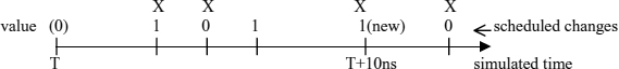
Figure 3.1 Assignment using an inertial 10 ns delay (‘X’: discarded change)
Listing 3.8 describes both the functional and the timing behavior of AND2 so that L-H transitions occur with a delay of 3 ns, H-L transitions with a delay of 2 ns, and no transitions occur in response to short input signal ‘spikes’ of less than 2 ns duration. This is the typical behavior of a CMOS AND gate. An alternative behavioral architecture for AND2 could e.g. use different timing data. Timing parameters can also be defined as ‘generic’ parameters for the entity. Similarly, the processing time of the adder or the delay of the output of a flip-flop or a register from the clock edge can be specified (Listings 3.3, 3.4, 3.5).
architecture fast of AND2 is
begin
       t <= ‘1’ after 3 ns      when ((r and s) =‘1’) else
            ‘0’ after 2 ns      when ((r and s) =‘0’);
end fast;
Listing 3.8 Functional and timing behavior of the AND gate
The correct operation of a D flip-flop or register requires that the data input should not transition at the time of the clock edge. It must not change between the set-up time before the edge and the hold time after the edge. If the data transitions during this time the behavior of the flip-flop is undefined (and may be non-deterministic for the circuits given in section 2.1.2). The VHDL definitions, however, define the behaviors of entities positively only. Listing 3.9 shows how an error message can be generated during the simulation if the set-up and hold times are violated. It uses the attribute s'last_event to obtain the time delay since the last change of a signal s.
process (clk,d)
begin
       if d'event then
               assert clk=‘0’or clk'last_event >= 1 ns
               report “hold time violated” severity warning;
      end if;

      if clk'event and clk=‘1’ then
              assert d'last_event >= 1 ns
              report “set-up time violated” severity warning;
              q <= d after 3 ns;
              nq <= not d after 3 ns;
      end if;
end process;
Listing 3.9 Flip-flop process checking for set-up and hold time violations
The definition in Listing 3.10 formally specifies the behavior of another basic circuit, the handshaking circuit for a reactive circuit using an output pipelining latch to store the data as long as OR = ‘1’ (see Figure 2.24). The generation of the delayed IR signal might be moved into a separate entity.
entity HS is
       generic exec_time: time;
       port(IR,OA: in bit; IA,OR: buffer bit);
end HS;

architecture timing of HS is
       signal IR_del: bit;
begin
       IR_del <= ‘1’ after exec_time when IR=‘1’ else ‘0’ after 3 ns;

       IA <= ‘1’ after 3 ns when IR_del=‘1’ and OR=‘0’ else
             ‘0’ after 3 ns when IR_del=‘0’else IA;
       OR <= ‘1’ after 3 ns when IR_del=‘1’ and OA=‘0’ else
             ‘0’ after 3 ns when OA=‘1’ else OR;
end timing;
Listing 3.10 Handshaking circuit behavior
3.6 TEST BENCHES
The behavior of a circuit defined in VHDL resulting from the time delays and conditions can be visualized with the aid of a VHDL simulator by connecting signal sources to the inputs of the circuit as stimulus signals. The signal sources and their connection to the circuit are defined within another VHDL program. Such a combined program is called a test bench for the circuit in question as it is analogous to connecting real signal sources to the circuit on a breadboard and measuring the output waveforms by means of a logic analyzer (Figure 3.2). Test benches have no external signals.
Test signals are easily generated by means of multiple timed assignments to them. A periodic clock can be generated through an assignment of the kind
clk <= not clk after 25 ns;
or by means of the process shown in Listing 3.11.
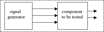
Figure 3.2 Test bench for a component
pn: process
       variable x: bit;
begin
       x := not x;
       a <= x;
       wait for 25 ns;
end process;
The definition in Listing 3.12 describes a test bench for the AND2 component defined in Listing 3.11. The circuit to be tested is included as a component into the test system. Its definition is supposed to be found in the standard library ‘work’.
entity test is end test;	                      -- there are no ports to the test system

architecture fast of test is
       component AND2 port(r,s: in bit; t: out bit) end component;
       signal a,b,c: bit;
begin
       c: AND2 port map (a,b,c);                      -- this line defines an instance of the type
                                                      AND2
       a <= ‘0’, ‘1’ after 10 ns, ‘0’ after 30 ns;    -- test signal definitions
       b <= ‘0’, ‘1’ after 20 ns, ‘0’ after 40 ns;
       end fast;                                      -- configure simulator to display a, b,
                                                      and c
Listing 3.12 Test bench for AND2
The assignments to a and b are all executed at the beginning of the simulation and specify particular time patterns for them. ‘a’ e.g. changes for T = 0 ns, 10 ns, and 30 ns and stays at ‘0’ afterwards. A simulator display showing a, b, and c for T = 0 .. 60 ns would be similar to Figure 3.3.
For complex input and output patterns, test data can be stored in files or be read from such. If memories need to be attached to a circuit (e.g. a programmable processor) to obtain an operating environment for it, they can be simulated in a test bench for it by means of arrays. They can be filled with initial data from some file at the start of the simulation, or by calling some initialization program. For testing application specific processors that read sequences of function codes (instructions) from a memory, it is necessary to initialize the memory with test sequences (programs). User-defined enumeration types can be used to support the symbolic input of such. After a definition such as
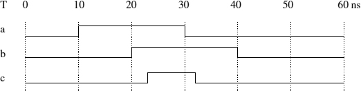
Figure 3.3 Simulator display for the AND2 signals
type opcode is (and, or, xor, not, add, sub, mul, div);
opcode symbols can be converted into function codes (using e.g. a case statement), and it is easy to implement an assembly function with a symbolic opcode argument that translates the opcodes and additional parameters into processor instructions and places them into subsequent locations of the memory array in the test bench.
3.7 SYNTHESIS ASPECTS
Besides specifying the structure and the behavior of a digital system up to the point of being able to simulate its operation, the information within a VHDL design is used to synthesize the hardware from certain basic components such as gates and flip-flops. VHDL synthesis results in a formal network description of such basic components submitted as a text file that lists the uses of component instances and their wiring through wire nets. A common format for this description is the EDIF net list format [42]. The structure and the contents of the EDIF net list are quite similar to a purely structural architecture definition in VHDL. It starts by listing the components and their interfaces, then proceeds to the interface definition of the entity, introduces the component instances to be used, and interconnects them through ‘nets’. For an FPGA design, this net list is used as the input to a FPGA specific software tools that map the gate and flip-flop functions to cell functions, map the required cells to the physical cells on a particular FPGA chip (placement), route the interconnections required by the design using the available wiring resources (routing), and finally encode the results in a bit stream for the FPGA that can be downloaded into its configuration memory. For the selected placement and routing, the signal delays and the processing delays can be determined from the timing parameters of the FPGA chip and checked to meet the performance requirements. The routed interconnections result in significant signal delays that do not depend on the circuit structure but on the particular usage of the routing resources. It is these timing data that must be used in the behavioral description of the system to be built in order to obtain a correct simulation of the actual circuit.
The net list is derived from the specified functional behavior and the structural information but does not depend on the delay data for the timing behavior (and on other structures only needed for the simulation). The net list constitutes a purely structural description of the hardware. It is derived from the supplied structural information in the architectures of the VHDL entities, but also attempts to be extracted from the functional specifications. The algorithms in the functions and processes are transformed into Boolean expressions for which a minimization is performed. The Boolean operators are transformed into gate instances. This extraction process from the functional specifications is no longer under the control of the designer. If there is e.g. an add operation for bit fields of the type ‘unsigned’ in the behavioral description as in Listing 3.3, it is not defined which adder circuit is actually realized in the net list (there are several choices, see section 4.2), and a user-defined add operation as in Listing 3.2 might not be recognized as such and be realized efficiently. If this control of the results of synthesis is desired, a structural specification of the entity must be given by the designer. Also, certain entities cannot be further resolved into networks, and their instances show up in the final net list. This is the case for memory arrays or the delay elements used for handshaking. If such entities adhere to specific patterns corresponding to FPGA structures such as memory blocks, the FPGA specific tools recognize their instances and map them to the corresponding FPGA resources. Their behavioral descriptions are uniquely intended for the simulation. To suppress synthesis from these, the entity and architecture definitions are enclosed between special VHDL comment lines that act as compiler switches, ‘-- RTL_SYNTHESIS OFF’ and ‘-- RTL_SYNTHESIS ON’ or equivalent ones recognized by the synthesis backend tool.
Synthesis from behavioral architectures also generates latch and flip-flop components for signals written to in processes and for process variables, yet no flip-flops clocked at both edges or by dual clock signals. There are some basic rules that determine whether signals and variables correspond to latches or to edge sensitive flip-flops that derive from the proposed standard [43]:
- a process variable always written to in a process before being read at most contributes a network of gates (a ‘combinatorial’ function);
- a variable always written to and sometimes read before corresponds to a registers (unless it is used for the simulation only);
- signals not read in the process and not written to under all conditions become latches;
- signals written to conditionally after ‘if clk’ event and clk=‘1’ then …' are registers; other branches not depending an on event may asynchronously set or reset the output;
- without clk'event latches are generated, even if ‘clk’ is the only signal in the sensitivity list.
The latch generation in the latter case is due to the fact that the synthesis tools automatically add the involved signals to the sensitivity list, including the signals from which the value to be assigned although the simulation would show the behavior of an edge-sensitive flip-flop. It is therefore common practice to always include such signals in the sensitivity lists.
Selective signal assignments according to the values of control signals generally translate into select circuits (multiplexers) although for some target architectures distributed selection through tri-state drivers attached to bus lines might be more advantageous. Bus lines need to be specified explicitly even in a behavioural definition. Other optimizations to a design such as sharing components like adders for different purposes also need to be specified through structural elements.
3.8 SUMMARY
VHDL is a common language to formally describe the structure and the behavior of digital systems and their components. It serves to simulate complex circuits, and to carry out hardware design using synthesis tools that automatically derive the needed components and their interconnections. In contrast to value assignments in software languages, assignments to signals are temporal processes and can occur at certain times only, e.g. after clock and handshaking events. If a signal is not assigned a value during some time, it holds the last value and behaves like a storage element. Our discussion reviewed the basic components such as gates and flip-flops. For gates, the processing delays in general depend on the output level, and registers and flip-flops need to respect set-up and hold times for the data inputs. Some VHDL constructs such as text output or file functions do not describe circuit structures but serve to implement test benches and to output results of the simulation.
EXERCISES
- Define the behavior of a flip-flop with a gated clock signal.
- Implement a test bench for a system of two cascaded instances of the HS entity in Listing 3.10 and verify their correct operation with suitable test signals, using a VHDL simulator.
- Define a variant of HS for which the pipelining latch is moved to the input of the reactive circuit.
- Define the behavior of an elementary gate or a flip-flop with std_logic inputs and output so that transitions have a non-zero rise or fall time modeled by an intermediate ‘W’ state of the signals and enforce a maximum rise time for the clock signal of the flip-flop. We remark that this kind of behavioral description still does not capture the actual circuit behavior of the involved signals as would be modeled by an analogue circuit simulator program (e.g., Spice) although it may be a better approximation than the zero-time change events.
- Define an entity that provides the interface signals of the 8-bit EPP peripheral bus found on PC workstations and distributes them to four separate input ports and an output port, using the address write cycle to select one of the input ports for subsequent data cycles. Such an interface is typical for accessing several circuits within an FPGA from the bus of an attached processor. For a peripheral circuit, the EPP signals are (see the specification in [71]):
- 8 bidirectional data lines
- data strobe input (chip enable signal as in Figure 2.36)
- address strobe input (alternative chip enable signal)
- read/write select input
- reset input
- interrupt output
- ready handshake output.
- Implement a simulation primitive that computes an ordered list of positive integers describing the simulated times of events on some signal from a sequence of lists of integers in which the first entries are the activation times and the subsequent ones are relative times for subsequent events, using transport delays only.