
CHAPTER 9
Ab Initio Molecular Dynamics Studies of Conjugated Dienes on Semiconductor Surfaces
MARK E. TUCKERMAN AND YANLI ZHANG
9.1 INTRODUCTION
The chemistry of hybrid structures composed of organic molecules and semiconductor surfaces is opening up exciting new areas of development in molecular electronics, nanoscale sensing devices, and surface lithography [1,2]. Covalent attachment of organic molecules to a semiconducting surface can yield active devices, such as molecular switches and sensors or passivating insulating layers. Moreover, it is intriguing to consider how the reactions might be controlled by “engineering” specific modifications to organic molecules and/or surfaces, suggesting possible new lithographic techniques.
One of the goals of controlling the surface chemistry is the creation of ordered nanostructures on semiconducting surfaces. Indeed, there has been some success in obtaining locally ordered structures on the hydrogen-terminated Si(100) surface [3–7]. These methods require a dangling Si bond without a hydrogen to initialize the self-replicating reaction. Another popular approach eliminates the initialization step by exploiting the reactivity between surface dimers on certain reconstructed surfaces with the π bonds in many organic molecules. The challenge with this approach lies in designing the surface and/or the molecule so as to eliminate all but one desired reaction channel. Charge asymmetries, such as occur on the Si(100)-2×1 surface, lead to a violation of the usual Woodward-Hoffman selection rules, which govern many purely organic reactions, allowing a variety of possible [4 + 2] and [2 + 2] surface adducts. Multiple reactive sites, such as occur on some of the SiC surfaces, also allow for a variety of possible adducts.
The exploration of hybrid organic-semiconductor materials and the reactions associated with them is an area in which theoretical and computational tools can play an important role. Indeed, modern theoretical methods combined with high-performance computing, have advanced to a level such that the thermodynamics and reaction mechanisms of a variety of chemical processes can now be routinely studied. These studies can aid in the interpretation of experimental results and can leverage theoretical mechanisms to predict the outcomes of new experiments. This chapter will focus on a description of one set of such techniques, namely, those based on density functional theory and first-principles or ab initio molecular dynamics (AIMD) [8–11]. As these methods employ an explicit representation of the electronic structure, electron localization techniques can be used to follow local electronic rearrangements during a reaction and, therefore, generate a clear picture of the reaction mechanism. In addition, statistical mechanical tools can be employed to obtain thermodynamic properties of the reaction products, including relative free energies and populations of the various products. Following a detailed description of the computational approaches, we will present a series of applications to conjugated dienes reacting with different semiconductor surfaces [12–17]. We will explore the role of surface thermal motions on the reaction mechanisms, and we will demonstrate how the predicted mechanisms can be used to rationalize product distributions [18]. We will investigate how the surface structure influences the thermodynamics of the reaction products and how these thermodynamic properties can be used to “reverse engineer” the molecule and/or the surface in order to control the product distribution and associated free energies. Finally, we will describe the problem of computing theoretical scanning tunneling microscopy (STM) images and the challenges inherent in simple perturbative schemes. Unless otherwise stated, all of the calculations to be presented in this chapter were carried out using the implementation of plane-wave based AIMD in the PINY_MD package [19]. Details of this methodology are presented in the next section.
9.2 COMPUTATIONAL METHODS
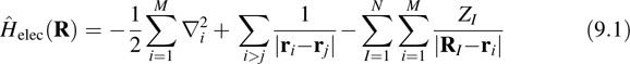
Because the problem of covalently attaching an organic molecule to a semiconductor surface requires the formation of chemical bonds, a theoretical treatment of this problem must be able to describe this bond formation process, which generally requires an ab initio approach in which the electronic structure is accounted for explicitly. Assuming the validity of the Born–Oppenheimer approximation, the goal of any ab initio approach is to approximate the ground-state solution of the electronic Schrodinger equation Ĥelec(R)|Ψ0(R)![]() = E0 (R)|Ψ0(R)
= E0 (R)|Ψ0(R)![]() , where Ĥelec is the electronic Hamiltonian, and R denotes a classical configuration of the chemical nuclei in the system. Ultimately, in order to predict reaction mechanisms and thermodynamics of a large, condensed-phase system, one needs to use approximate solutions of the Schrodinger equation and based on these solutions, propagate the nuclei dynamically using Newton's laws of motion. This is the essence of the method known as ab initio molecular dynamics (AIMD) [8–11].
, where Ĥelec is the electronic Hamiltonian, and R denotes a classical configuration of the chemical nuclei in the system. Ultimately, in order to predict reaction mechanisms and thermodynamics of a large, condensed-phase system, one needs to use approximate solutions of the Schrodinger equation and based on these solutions, propagate the nuclei dynamically using Newton's laws of motion. This is the essence of the method known as ab initio molecular dynamics (AIMD) [8–11].
In this section, we will briefly review density functional theory (DFT) as the electronic structure method of choice for the studies to be described in this chapter. DFT represents a compromise between accuracy and computational efficiency. This is an important consideration, as a typical AIMD calculation requires that the electronic structure problem be solved tens of thousands to hundreds of thousands of time in order to generate one or more trajectories of sufficient length to extract dynamic and thermodynamic properties. We will then describe the AIMD approach, including several technical considerations such as basis sets, boundary conditions, and electron localization schemes.
9.2.1 Density Functional Theory
As previously above, we seek approximate solutions to the electronic Schrödinger equation. To this end, we begin by considering a system of N nuclei at positions R1, …, RN ≡ R and M electrons with coordinate labels r1,…,rM and spin states s1,…,sM. The fixed nuclear positions allow us to define the electronic Hamiltonian (in atomic units) as
where ZI is the charge on the Ith nucleus. The first term in Equation 9.1 represents the electron kinetic energy, the second represents the electron–electron Coulomb repulsion, and the third represents the electron–nuclear Coulomb attraction. The time-independent electronic Schrödinger equation or electronic eigenvalue problem
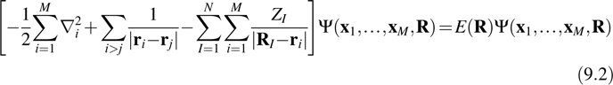
must be solved in order to generate all of the electronic energy levels and eigenfunctions at the given nuclear configuration R. Here xi = ri, si is a combination of coordinate and spin variables. Unfortunately, for large condensed-phase problems of the type to be considered here, an exact solution of the electronic eigenvalue problem is computationally intractable.
The Kohn–Sham (KS) [20] formulation of density functional theory (DFT) [21] replaces the fully interacting electronic problem in, Equation 9.2 by an equivalent noninteracting system that is required to yield the same ground-state energy and ground state electronic density as the original interacting system. As the name implies, the central quantity in DFT is this ground-state electron density n0(r) generated from the ground-state electronic wave function Ψ0 via
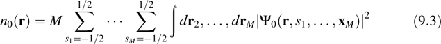
where, for notational convenience, the dependence on R is left off. The central theorem of DFT is the Hohenberg–Kohn theorem, which states that there exists an exact energy E[n] that is a functional of electronic densities n(r) such that when E[n] is minimized with respect to n(r) subject to the constraint that ∫ dr n(r) = M (each n(r) must yield the correct number of electrons), the true ground-state density n0(r) is obtained. The true ground-state energy is then given by E0 = E[n0]. (Remember that E0 is a function of nuclear positions: E0 = E0(R).) The KS noninteracting system is constructed in terms of a set of mutually orthogonal single-particle orbitals ψi(r) in terms of which the density n(r) is given by
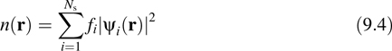
where fi are the occupation numbers of a set of Ns such orbitals, where Σi fi = M. In closed-shell systems, the orbitals are all doubly occupied so that Ns = M/2, and fi = 2. In open-shell systems, we treat all of the electrons in double and singly occupied orbitals explicitly and take Ns = M. When virtual or unoccupied orbitals are needed, we can take Ns > M/2 or Ns > M for closed-and open-shell systems, respectively, and take fi = 0 for the virtual orbitals.
In KS theory, the energy functional is taken to be
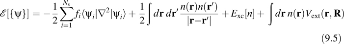
The first term in the functional represents the noninteracting quantum kinetic energy of the electrons, the second term is the direct Coulomb interaction between two charge distributions, the third term is the exchange-correlation energy, whose exact form is unknown, and the fourth represents the “external” Coulomb potential on the electrons due to the fixed nuclei, ![]() Minimization of Equation 9.5 with respect to the orbitals subject to the orthogonality constraint leads to a set of coupled self-consistent field equations of the form
Minimization of Equation 9.5 with respect to the orbitals subject to the orthogonality constraint leads to a set of coupled self-consistent field equations of the form
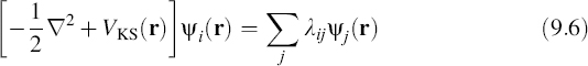
where the KS potential VKS(r) is given by

and λij is a set of Lagrange multipliers used to enforce the orthogonality constraint ![]() ψi|ψj
ψi|ψj![]() = δij. If we introduce into Equation 9.6 a unitary transformation U that diagonalizes the matrix λij, then we obtain the Kohn–Sham equations in the form
= δij. If we introduce into Equation 9.6 a unitary transformation U that diagonalizes the matrix λij, then we obtain the Kohn–Sham equations in the form
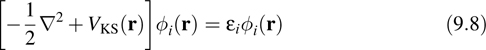
where ![]() are the KS orbitals and εi are the KS energy levels, that is, the eigenvalues of the matrix λij. If the exact exchange-correlation functional were known, the KS theory would be exact. However, because Exc[n] is unknown, approximations must be introduced for this term in practice. The accuracy of DFT results depends critically on the quality of the approximation. One of the most widely used forms for Exc [n] is known as the generalized-gradient approximation (GGA), where in Exc [n] is approximated as a local functional of the form
are the KS orbitals and εi are the KS energy levels, that is, the eigenvalues of the matrix λij. If the exact exchange-correlation functional were known, the KS theory would be exact. However, because Exc[n] is unknown, approximations must be introduced for this term in practice. The accuracy of DFT results depends critically on the quality of the approximation. One of the most widely used forms for Exc [n] is known as the generalized-gradient approximation (GGA), where in Exc [n] is approximated as a local functional of the form
where the form of the function fGGA determines the specific GGA approximation. Commonly used GGA functionals are the Becke–Lee–Yang–Parr (BLYP) [22,23] and Perdew–Burke–Ernzerhof (PBE) [24] functionals.
9.2.2 Ab Initio Molecular Dynamics
Solution of the KS equations yields the electronic structure at a set of fixed nuclear positions R1,…,RN ≡ R. Thus, in order to follow the progress of a chemical reaction, we need an approach that allows us to propagate the nuclei in time. If we assume the nuclei can be treated as classical point particles, then we seek the nuclear positions R1(t), RN(t) as functions of time, which are given by Newton's second law
where MI and FI are the mass and total force on the Ith nucleus. If the exact ground-state wave function Ψ0(R) were known, then the forces would be given by the Hellman–Feynman theorem
where we have introduced the nuclear–nuclear Coulomb repulsion potential
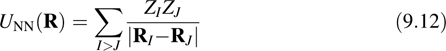
Within the framework of KS DFT, the force expression becomes
The equations of motion, Equations 9.10, are integrated numerically using a set of discrete times t = 0, Δt, 2 Δt,…, PΔt subject to a set of initial coordinates R1(0),…, RN(0) and velocities ![]() 1(0), …,
1(0), …, ![]() N(0) for a solver such as the velocity Verlet algorithm:
N(0) for a solver such as the velocity Verlet algorithm:
where FI (0) and FI (Δt) are the forces at t = 0 and t = Δt, respectively. Iteration of Equation 9.14 yields a full trajectory of P steps. Equations 9.13 and 9.14 suggest an algorithm for generating the finite-temperature dynamics of a system using forces generated from electronic structure calculations performed “on the fly” as the simulation proceeds: Starting with the initial nuclear configuration, one minimizes the KS energy functional to obtain the ground-state density, and Equation 9.13 are used to obtain the initial forces. These forces are then used to propagate the nuclear positions to the next time step using the first of Equation 9.14. At this new nuclear configuration, the KS functional is minimized again to obtain the new ground-state density and forces using Equation 9.13, and these forces are used to propagate the velocities to time t = Δt. These forces can also be used again to propagate the positions to time t = 2 Δt. The procedure is iterated until a full trajectory is generated. This approach is known as “Born–Oppenheimer” dynamics because it employs, at each step, an electronic configuration that is fully quenched to the ground-state Born–Oppenheimer surface.
An alternative to Born–Oppenheimer dynamics is the Car–Parrinello (CP) method [8–10]. In this approach, an initially minimized electronic configuration is subsequently “propagated” from one nuclear configuration to the next using a fictitious Newtonian dynamics for the orbitals. In this “dynamics”, the orbitals are given a small amount of fictitious thermal kinetic energy and are made “light” compared to the nuclei. Under these conditions, the orbitals actually generate a potential of mean force surface that is very close to the true Born–Oppenheimer surface. The equations of motion of the CP method are
where μ is a mass-like parameter for the orbitals (which actually has units of energy × time2), and λij is the Lagrange multiplier matrix that enforces the orthogonality of the orbitals as a holonomic constraint on the fictitious orbital dynamics. Choosing μ small ensures that the orbital dynamics is adiabatically decoupled from the true nuclear dynamics, thereby allowing the orbitals to generate the aforementioned potential of mean force surface. For a detailed analysis of the CP dynamics, see Refs. [10,25]. As an illustration of the CP dynamics, Fig. 1 of Ref. [26] shows the temperature profile for a short CPAIMD simulation of bulk silicon together with the kinetic energy profile from the fictitious orbital dynamics. The figure demonstrates that the orbital dynamics is essentially a “slave” to the nuclear dynamics, which shows that the electronic configuration closely follows the dynamics of the nuclei in the spirit of the Born–Oppenheimer approximation.
9.2.3 Plane Wave Bases and Surface Boundary Conditions
In AIMD calculations, the most commonly employed boundary conditions are periodic boundary conditions, in which the system is replicated infinitely in all three spatial directions. This is clearly a natural choice for solids and is particularly convenient for liquids. In an infinite periodic system, the KS orbitals become Bloch functions of the form
where k is a vector in the first Brioullin zone and uik(r) is a periodic function. A natural basis set for expanding a periodic function is the Fourier or plane-wave basis set, in which uik(r) is expanded according to
where V is the volume of the cell, g = 2πh−1ĝ is a reciprocal lattice vector, h is the cell matrix, whose columns are the cell vectors (V = det(h)), ĝ is a vector of integers, and {cki,g} are the expansion coefficients. An advantage of plane waves is that the sums needed to go back and forth between reciprocal space and real space can be performed efficiently using fast Fourier transforms (FFTs) if the orbitals are represented on a regular lattice. In general, the properties of a periodic system are only correctly described if a sufficient number of k-vectors are sampled from the Brioullin zone. However, for the applications we will consider, we are able to choose sufficiently large system sizes that we can restrict our k-point sampling to the single point, k = (0, 0, 0), known as the Γ-point. At the Γ-point, the plane-wave expansion reduces to
At the Γ-point, the orbitals can always be chosen to be real functions. Therefore, the plane-wave expansion coefficients satisfy the following property
which requires keeping only half of the full set of plane-wave expansion coefficients. In actual applications, plane waves up to a given cutoff |g|2/2 < Ecut only are retained. Similarly, the density n(r) given by Equation 9.4 can also be expanded in a plane-wave basis:
However, since n(r) is obtained as a square of the KS orbitals, the cutoff needed for this expansion is 4Ecut for consistency with the orbital expansion.
At first glance, it might seem that plane waves are ill-suited to treat surfaces because surfaces are naturally periodic in only two dimensions. However, in a series of papers, [27–29] Martyna, Tuckerman, and coworkers showed that clusters (systems with no periodicity), wires (systems with one periodic dimension), and surfaces (systems with two periodic dimensions) could all be treated using a plane-wave basis within a single unified formalism as follows. Let n(r) be a particle density with a Fourier expansion given by Equation 9.20, and let ϕ(r−r′) denote an interaction potential. In a fully periodic system, the energy of a system described by n(r) and ϕ(r−r′) is given by

where ![]() g is the Fourier transform of the potential. For systems with fewer than three periodic dimensions, the idea is to replace Equation 9.21 with its first-image approximation
g is the Fourier transform of the potential. For systems with fewer than three periodic dimensions, the idea is to replace Equation 9.21 with its first-image approximation
where ![]() g denotes a Fourier expansion coefficient of the potential in the nonperiodic dimensions and a Fourier transform along the periodic dimensions. For clusters,
g denotes a Fourier expansion coefficient of the potential in the nonperiodic dimensions and a Fourier transform along the periodic dimensions. For clusters, ![]() g is given by
g is given by
for wires, it becomes
The error in the first-image approximation drops off as a function of the volume, area, or length in the nonperiodic directions, as analyzed in Refs. [27–29].
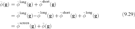
In order to have an expression that is easily computed within the plane-wave description, consider two functions ϕlong(r) and ϕshort(r), which are assumed to be the long- and short-range contributions to the total potential, that is,
The Fourier expansion coefficients, therefore, also satisfy this decomposition:
We require that ϕshort(r) vanish exponentially quickly at large distances from the center of the parallelepiped and that ϕlong(r) contain the long-range dependence of the full potential, ϕ (r) . With these two requirements, it is possible to write
with exponentially small error, ε(g), provided the range of ϕshort(r) is small compared to the size of the parallelepiped. In order to ensure that Equation 9.28 is satisfied, a convergence parameter, α, is introduced that can be used to adjust the range of ϕshort (r) such that ε(g) ~ 0 and the error, ε(g), will be neglected in the following.
The function, ![]() ~short(g), is the Fourier transform of ϕshort(r). Therefore,
~short(g), is the Fourier transform of ϕshort(r). Therefore,
where ![]() is the Fourier transform of the full potential,
is the Fourier transform of the full potential, ![]() and
and
Thus, Equation 9.30 becomes
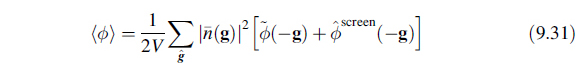
The new function appearing in the average potential energy, Equation 9.31, is the difference between the Fourier series and Fourier transform form of the long-range part of the potential energy and is referred to as a screening function because it is constructed in order to “screen” the interaction of the system with an infinite array of periodic images. The specific case of the Coulomb potential,
can be separated into short- and long-range components via
where erf(x) and erfc(x) are the error function and its complement, respectively:
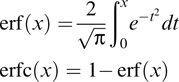
The first term in Equation 9.33 is long range. The parameter α determines the specific ranges of these terms. The screening function for the cluster case is easily computed by introducing an FFT grid and performing the integration numerically [27]. For the wire [28] and surface [29] cases, analytical expressions can be worked out. In particular, for surfaces, the screening function is
When a plane-wave basis set is employed, the external energy is made somewhat complicated by the fact that very large basis sets are needed to treat the rapid spatial fluctuations of core electrons. Therefore, core electrons are often replaced by atomic pseudopotentials or augmented plane-wave techniques. Here, we shall discuss the former. In the atomic pseudopotential scheme, the nucleus plus the core electrons are treated in a frozen core type approximation as an “ion” carrying only the valence charge. In order to make this approximation, the valence orbitals, which, in principle must be orthogonal to the core orbitals, must see a different pseudopotential for each angular momentum component in the core, which means that the pseudopotential must generally be nonlocal. In order to see this, we consider a potential operator of the form
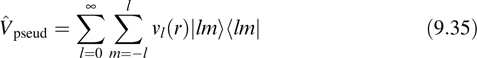
where r is the distance from the ion, and |lm)![]()
![]() lm| is a projection operator onto each angular momentum component. In order to truncate the infinite sum over l in Equation 9.35, we assume that for l greater than or equal to some l some, νl(r) ≈ νl(r) and add and subtract the function νl(r) in Equation 9.35:
lm| is a projection operator onto each angular momentum component. In order to truncate the infinite sum over l in Equation 9.35, we assume that for l greater than or equal to some l some, νl(r) ≈ νl(r) and add and subtract the function νl(r) in Equation 9.35:
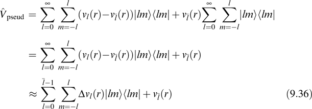
where the second line follows from the fact that the sum of the projection operators is unity, Δvl(r) = νl(r)−νl(r), and the sum in the third line is truncated before Δνl(r) = 0. The complete pseudopotential operator is

where νloc(r) ≡ νl(r) is known as the local part of the pseudopotential (having no projection operator attached to it). Now, the external energy, being derived from the ground-state expectation value of a one-body operator, is given by
The first (local) term gives simply a local energy of the form
which can be evaluated in reciprocal space as
where ![]() loc(g) is the Fourier transform of the local potential. Note that at g = (0, 0, 0), only the nonsingular part of
loc(g) is the Fourier transform of the local potential. Note that at g = (0, 0, 0), only the nonsingular part of ![]() loc(g) contributes. In the evaluation of the local term, it is often convenient to add and subtract a long-range term of the form ZIerf (αIr) /r, where erf(x) is the error function, for each ion in order to obtain the nonsingular part explicitly and a residual short-range function
loc(g) contributes. In the evaluation of the local term, it is often convenient to add and subtract a long-range term of the form ZIerf (αIr) /r, where erf(x) is the error function, for each ion in order to obtain the nonsingular part explicitly and a residual short-range function ![]() for each ionic core.
for each ionic core.
9.2.4 Electron Localization Methods
An important feature of the KS energy functional is the fact that the total energy E[{ψ}, R] is invariant with respect to a unitary transformation within the space of occupied orbitals. That is, if we introduce a new set of orbitals ψ′i(r) related to the ψi(r) by
where Uij is Ns × Ns unitary matrix, then the energy ![]() We say that the energy is invariant with respect to the group SU(Ns), that is, the group of all Ns × Ns unitary matrices with unit determinant. This invariance is a type of gauge invariance, specifically that in the occupied orbital subspace. The fictitious orbital dynamics of the AIMD scheme as written in Equation 9.15 does not preserve any particular unitary representation or gauge of the orbitals but allows the orbitals to mix arbitrarily according to Equation 9.41. This mixing happens intrinsically as part of the dynamics rather than by explicit application of the unitary transformation.
We say that the energy is invariant with respect to the group SU(Ns), that is, the group of all Ns × Ns unitary matrices with unit determinant. This invariance is a type of gauge invariance, specifically that in the occupied orbital subspace. The fictitious orbital dynamics of the AIMD scheme as written in Equation 9.15 does not preserve any particular unitary representation or gauge of the orbitals but allows the orbitals to mix arbitrarily according to Equation 9.41. This mixing happens intrinsically as part of the dynamics rather than by explicit application of the unitary transformation.
Although this arbitrariness has no effect on the nuclear dynamics, it is often desirable for the orbitals to be in a particular unitary representation or gauge. For example, we might wish to have the true Kohn–Sham orbitals ϕi(r) (see Equation 9.8) at each step in an AIMD simulation in order to calculate the Kohn–Sham eigenvalues and generate the corresponding density of states from a histogram of these eigenvalues. This would require choosing Uij to be the unitary transformation that diagonalizes the matrix of Lagrange multipliers in Eq. 9.6. Another important representation is that in which the orbitals are maximally localized in real space. In this representation, the orbitals are closest to the classic “textbook” molecular orbital picture.
In order to obtain the unitary transformation Uij that generates maximally localized orbitals, we seek a functional that measures the total spatial spread of the orbitals. One possibility for this functional is simply to use the variance of the position operator ![]() with respect to each orbital and sum these variances:
with respect to each orbital and sum these variances:
The procedure for obtaining the maximally localized orbitals is to introduce the transformation in Equation 9.41 into Equation 9.42 and then to minimize the spread functional with respect to Uij:
The minimization must be carried out subject to the constraint that Uij be an element of SU(Ns). This constraint condition can be eliminated if we choose U to have the form
where A is an Ns × Ns Hermitian matrix, and performing the minimization of Ω with respect to A.
A little reflection reveals that the spread functional in Equation 9.42 is actually not suitable for periodic systems. The reason for this is that the position operator ![]() lacks the translational invariance of the underlying periodic supercell. A generalization of the spread functional that does not suffer from this deficiency is [30,31]
lacks the translational invariance of the underlying periodic supercell. A generalization of the spread functional that does not suffer from this deficiency is [30,31]
where σ and L denote the typical spatial extent of a localized orbital and box length, respectively, and
Here GI = 2π(h−1)TĝI, where ĝI = (lI, mI, nI) is the Ith Miller index and ωI is a weight having dimensions of (length)2. The function f (|z|2) is often taken to be 1 – |z|2, although several choices are possible. The orbitals that result from minimizing Equation 9.45 are known as Wannier orbitals|wi![]() . If zI,ii is evaluated with respect to these orbitals, then the orbital centers, known as Wanner centers, can be computed according to
. If zI,ii is evaluated with respect to these orbitals, then the orbital centers, known as Wanner centers, can be computed according to
Wannier orbitals and their centers are useful in analyzing chemically reactive systems and will be employed in the present surface chemistry studies.
Like the KS energy, the Lagrangian that generates the fictitious, CP dynamics is invariant with respect to gauge transformations of the form given in Eq. 9.41. It is not, however, invariant under time-dependent unitary transformations of the form
and consequently, the orbital gauge changes at each step of an AIMD simulation. If, however, we impose the requirement of invariance under Equation 9.48 on the CP Lagrangian, then not only would we obtain a gauge-covariant version of the AIMD algorithm, but we could also then fix a particular orbital gauge and have this gauge be preserved under the CP evolution. Using techniques for gauge field theory, it is possible to devise such a AIMD algorithm [32]. Introducing orbital momenta |πi![]() conjugate to the orbital degrees of freedom, the gauge-covariant AIMD equations of motion have the basic structure
conjugate to the orbital degrees of freedom, the gauge-covariant AIMD equations of motion have the basic structure
Where
Here, the terms involving the matrix Bij (t) are gauge-fixing terms that preserve a desired orbital gauge. If we choose the unitary transformation Uij (t) to be the matrix that satisfies Equation 9.43, then Equation 9.49 will propagate maximally localized orbitals [33]. As was shown in Refs. [32,33], if it possible to evaluate the gauge-fixing terms in a way that does not require explicit minimization of the spread functional [34]. In this way, if the orbitals are initially localized, they remain localized throughout the trajectory. Explicit expressions for Bij are given in Ref. [32].
While the Wannier orbitals and Wannier centers are useful concepts, it is also useful to have a measure of electron localization that does not depend on a specific orbital representation, as the latter does have some arbitrariness associated with it. An alternative measure of electron localization that involves only the electron density n(r) and the so-called kinetic energy density
was introduced by Becke and Edgecombe [35]. Defining the ratio
Where
the function
can be shown to lie in the interval f(r) ∈ [0,1], where f (r) = 1 corresponds to perfect localization, and f (r) = 1/2 corresponds to a gas-like localization. The function f(r) is known as the electron localization function or ELF. In the studies to be presented below, we will make use both of the ELF and the Wannier orbitals and centers to quantify electron localization.
9.3 REACTIONS ON THE SI(100)-(2×1) SURFACE
When solid silicon is cleaved along its (100) plane, the dangling atoms reconstruct in such a way that parallel rows of silicon dimers are formed. This is the well-known 2 × 1 reconstruction. The Si–Si bond in these surface dimers consists of a σ bond and a weak, partial π bond, so that the bond order is less than 2. Nevertheless, there is sufficient π character in the dimers for them to act as dieneophiles in reactions with conjugated dienes of the type that we will consider in this section.
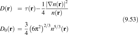
Experiments [36,37] have shown that the surface dimers do not lie in a single plane but preferentially form a buckled c(4 × 2) structure, in which neighboring dimers in each row buckle in opposite directions and in which neighboring rows are mirror images of each other (see Figure 9.1 (top) and (bottom)). Low-temperature scanning tunneling microscopy has identified the persistence of this buckled structure down to temperatures below 10 K [37]. The buckling gives rise to a polarization of the Si–Si bond, with the lower silicon atom acquiring a net positive charge and the upper silicon acquiring a net negative charge (see Figure 9.2). At room temperature, the buckling pattern is dynamic with the dimers executing a “rocking” motion or oscillation about the idealized pattern in Fig. 9.1(top). Electron energy loss spectroscopy (EELS) [38] gives a dimer rocking frequency of 20 meV or ~200 fs at 300 K but does not reveal how frequently the dimer flips to the opposite orientation. Ab initio [39] and force field-based [40,41] molecular dynamics simulations confirm the rocking period is between 200 and 300 fs, while the flipping period ranges from 200 fs to more than 1.5 ps. We will see that the charge asymmetry in the dimers and the surface dynamics influence both the reaction mechanisms and the reaction kinetics.
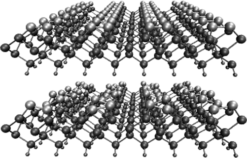
FIGURE 9.1 (Top) Symmetric dimers on the Si(100)-(2 × 1) surface. (Bottom) Buckled dimers on the Si(100)-(2 × 1) surface.
As a tangential point, we briefly comment on the zero-temperature surface structure. The point is tangential because all of the calculations to be presented are at 300 K where the buckling and dimer flipping are well-established surface characteristics. At T = 0, however, there is a discrepancy between DFT and high-level quantum chemical approaches that include multireference methods. The former can be carried out in a well-converged plane-wave basis with the periodicity of the surface properly accounted for. The latter, while more accurate in their treatment of the electgronic structure, can only be carried out on small clusters that contain one or two Si–Si dimers, which is a crude representation of the surface. Interestingly, the DFT calculations yield the buckled configuration as the zero-temperature structure [15], in agreement with the low-temperature STM [37], while the cluster calculations yield the symmetric unbuckled structure [42]. It is not obvious whether the source of the discrepancy is due primarily to the level of accuracy of the two approaches and possible fortuitous cancellation of errors in the DFT calculations, or whether the dimer-dimer interactions and surface periodicity are critical in stabilizing the buckled structure.
It is also worth mentioning that the lattice constant of bulk silicon and Si–Si dimer length on the Si(100)-(2 × 1) surface in DFT depend somewhat on the exchange-correlation functional employed. Two popular choices are the BLYP [22,23] and PBE [24] functionals. BLYP gives a bulk lattice constant of 5.52 Å and a surface dimer bond length of 2.3 Å at 300K. PBE gives a bulk lattice constant of 5.47 Å, in better agreement with the experimental value of 5.43Å, [43] and a dimer bond length of 2.3 Å at 300K. Thus, overall, the PBE functional is somewhat better for treating the silicon surface, but even BLYP provides a reasonable description. In what follows, we will present results employing both functionals.
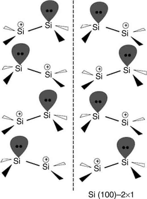
FIGURE 9.2 Diagram of the c(4 × 2) structure of the Si(100)-(2 × 1) surface showing the charge asymmetry within the surface dimers.
9.3.1 Attachment of 1,3-Butadiene to the Si(100)-(2 × 1) Surface
The first reaction we will discuss is the covalent attachment of 1,3-butadiene to the Si(100)-(2×1) surface. This benchmark system has been studied both experimentally and theoretically [12,13,44–48]. In addition, it is electronically similar to the conjugated region of the 1,3-cyclohexadiene molecule, which has been investigated using STM, [18,49] thus making comparisons with these measurements possible (see Figure 9.3). Because experiments and static ab initio calculations cannot identify specific mechanisms by which these addition products form, this system is ideal to study using AIMD.
We begin by describing a calculation aimed at probing the distribution of products formed when 1,3-butadiene reacts with the surface. AIMD calculations were performed on a system of four silicon layers composed of 32 atoms (four surface dimers), a passivating bottom layer of hydrogens, and one cis-1,3-butadiene at a temperature of 300K. The electronic structure was represented using the BLYP exchange-correlation functional. The KS orbitals were expanded in a plane-wave basis at the Γ-point, with Troullier–Martins atomic pseudopotentials [50] up to a cutoff of 35 Ry, which is sufficient to converge the geometry of the butadiene and reproduce the change in energy per surface dimer (~ −1.5 eV) upon reconstruction, in reasonable agreement with experiment [51] and other theoretical estimates [52]. Our proper treatment of the surface boundary conditions allowed a box with periodic dimensions 15.34, 7.67 Å, and nonperiodic dimension 22.53 Å to be used. Because the system is highly reactive, we employed a modified version of the Car--Parrinello AIMD algorithm that constrains the fictitious electronic kinetic energy in the CP Lagrangian to a preset value [53]. In order to generate a meaningful product distribution, 40 trajectories, each of length 2–3 ps, were initiated from an unbiased distribution of initial configurations of the butadiene above the surface. In total, roughly 110 ps of trajectory data were generated.
FIGURE 9.3 The two conjugated dienes considered in this chapter.
In Figure 9.4, we show snapshots of the different addition products obtained from the trajectory ensemble. The small spheres in the bond between atoms are the centers of the maximally localized Wannier functions, and the isosurface shown in panels (a), (c), (d), and (f) is the 0.95 isosurface of the ELF. In addition, each panel contains one or more darkly colored spheres (see Ref. [13] for a color version of Figure 9.4); these designate local fully or partially positively charged sites. Product A (shown in panel (a)) is a [4+2] product in which the butadiene attaches to a single Si–Si dimer. The two Wannier centers between Carbons C2 and C3 indicate a double bond between these two carbons, and the single Wannier center between the two silicon atoms in the Si–Si dimer to which the butadiene is attached indicates a single bond. Hence, product A is essentially the analog of a Diels–Alder adduct in which the Si–Si dimer plays the role of the ethylene reactant (see Figure 9.5). Product B (shown in panel (b)) is an intrarow, interdimer [4+2] product, in which the butadiene attaches to two dimers within a single row. Once again, the presence of two Wannier centers between carbons C2 and C3 indicates the conversion of the single C–C bond to a double bond in the final product. Product C (shown in panel (c)) is an interrow, interdimer [4+2] product, in which the butadiene bridges two dimers in neighboring rows. Product D (shown in panel (d)) is a [2+2] product in which carbons C1 and C2 bridge two dimers in a single row. Notice, in this, case that there are two Wannier centers between Carbons C3 and C4, indicating that this double bond, which normally exists in 1,3-butadiene, remains in tact. Panel (e) shows an intermediate “fluxional” species that can occur after the formation of a [2+2] adduct when the C3 = C4 double bond is positioned for a second nucleophilic attack. This species rapidly converts to a stable [4+2]-like interdimer adduct via an electron pair reorganization. Finally, panel (f) shows a stable intermediate carbocation state that forms in most of the reactions observed. Such carbocation intermediates have been observed STM measurements, [54] and we will have more to say about this species below.
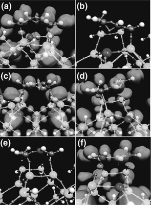
FIGURE 9.4 Snapshots of the addition products obtained. Large, medium, and small spheres denote Si, C, and H atoms, respectively, and very small spheres in bonds between atoms indicate the location of Wannier centers. Darkly shaded spheres locate atoms with positive full or partial charge. Full positive charge is defined to be an atom surrounded by three Wannier centers. The surface is the ELF 0.95 isosurface. A full color version of this figure can be found in Ref. [13].
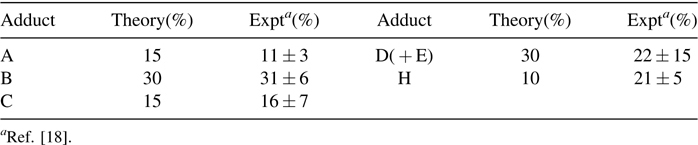
From the ensemble of trajectories, we can predict the product distribution for comparison with STM measurements on 1,3-cyclohexadiene [18]. This distribution, reported in Table 9.1, shows the percentages of the addition products together with the experimental values for 1,3-cyclohexadiene. In Table 9.1, the “H” population is the fraction of the ensemble that did not form a definite product on the time scale of the simulations, while in the STM measurement, it designates all adducts that could not be identified as one of A–E. Generally, it can be seen that the yields of all products analogous to those of Ref. [18], that is, A–D(+E), agree with experiment within the error bars. Some slight differences between the 1,3-butadiene and 1,3-cyclohexadiene products are (1) for the former, the B adduct forms diagonally across two intrarow dimers and (2) the [2+2] adduct is actually an interdimer [2+2]-like adduct within a row.
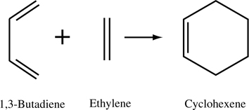
FIGURE 9.5 Classic Diels–Alder reaction between 1,3-butadiene and ethylene yielding cyclohexene.
TABLE 9.1 Final Product Distribution
In order to rationalize the distribution observed in the STM measurement and in the AIMD calculations, we next focus on the mechanism of these cycloaddition reactions. Figure 9.6 shows the carbon–carbon and carbon–silicon bond distances as functions of time over a typical trajectory that leads to the Diels–Alder [4+2] intradimer product. It can be seen that, of the two C = C double bonds, one reverts to a single bond before the other. This is consistent with the formation of the carbocation intermediate shown in panel (f) of Figure 9.4. Similarly, one of the Si–C bonds forms before the other. These bond-length trajectories, which are similar to those seen in many of the ensemble members, suggest an asymmetric, non-concerted mechanism that proceeds via the carbocation intermediate.
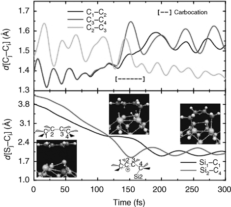
FIGURE 9.6 Si–C and C–C bond lengths versus simulation time for a representative trajectory leading to the [4+2] Diels–Alder adduct. From left to right the three snapshots depict: (i) butadiene above the Si(100)-(2 × 1) surface, (ii) carbocation formation, (iii) final [4+2] DA adduct. Sphere coloring is the same as in Figure 9.4. A full color version of this figure can be found in Ref. [13].
To this end, we have proposed the following mechanism [13] that serves to rationalize the observed product distribution both in the AIMD trajectory ensemble and in the STM measurements. This mechanism is illustrated in the scheme of Figure 9.7.
The mechanism, which is common to all of the reactions simulated, begins with a nucleophilic attack of the C = C double bond on the positively charge atom in one of the Si–Si dimers. The subsequent migration of the local positive charge from the Si atom, now neutralized by formation of the Si–C bond, dictates the outcome of the reaction. In all cases, the next step involves the migration of the positive charge into the organic molecule, leading to a carbocation intermediate (Figure 9.7R). The carbocation, which can exist for up to 1–2 ps, is stabilized by resonance, as illustrated by the three ELF lobes and the three Wannier centers around the positive carbon atoms. The Wannier center of the delocalized orbital is located below the middle carbon atom, indicating that it is shared by two bonds. Since the carbocation bonds to an Si atom of a surface dimer and the other dimer member has a net negative charge, an intermediate zwitterionic state is formed. In one of the resonant structures, the positive charge is “localized” on the end of the butadiene (Figure 9.7R-right), which allows the carbon to attack the negatively charged Si atom. This leads to the formation of the Diels–Alder [4+2] adduct in panel (a) of Figure 9.4.
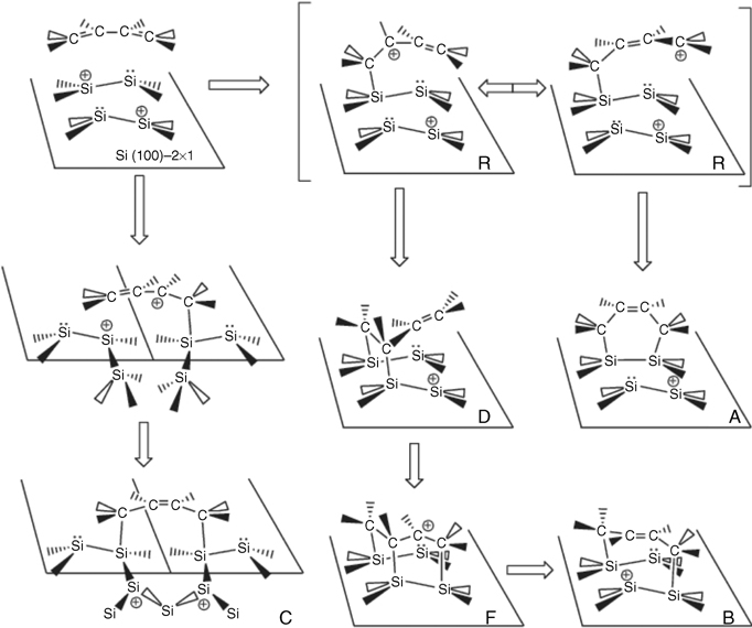
FIGURE 9.7 Scheme depicting the proposed reaction mechanism of 1,3-butadiene with the Si(100)-(2 × 1) surface.
If we consider the resonant structure in which the double bond is localized on the end of the butadiene (Figure 9.7R-right), then the positive carbon can attack the negatively charged Si of a neighboring dimer. This leads to the interrow [2+2]-like adduct in panel (d) of Figure 9.4. If the remaining double bond in the butadiene is positioned for a second nucleophilic attack, then the fluxional intermediate (panel (e) of Figure 9.4) is formed, and this intermediate is seen to convert rapidly to the final [4+2] product. The fluxional intermediate was also suggested in the STM measurements of Ref. [18]. The [2+2]-like product is stabilized if the double bond at the end of the butadiene is oriented between the rows. Finally, the inter-row adduct formation is initiated by a second nucleophilic attack of the C = C double bond in the zwitterion on the positively charged Si atom in a neighboring row. This product constitutes a nine-membered ring, which is accompanied by migration of the local positive charge into the bulk layer as seen in the ELF isosurface in panel (c) of Figure 9.4.
The preceding discussion highlights the predominance of a stepwise zwitterionic mechanism governing addition product formation on the Si(100)-(2 × 1) surface. Although we cannot rule out a concerted mechanism, one might expect on statistical grounds that the initially asymmetric charge distribution in the surface dimers allows only very special initial conditions to lead to a concerted reaction path. In fact, one of the trajectories in the ensemble exhibited a concerted path, however, as we will see in the free energy analysis to follow, this type of mechanism is not a highly probability event in the ensemble. This suggests that the mechanism of the Diels–Alder adduct formation is dominated by a nonconcerted mechanism, indicating that on the Si(100)-(2 × 1) surface, the usual Woodward–Hoffman rules governing organic cycloaddition reactions [55] do not necessarily apply [13,15]. Specifically, the charge asymmetry allows for the violation and leads to the observed distribution of surface adducts.
We can explore the reaction mechanism in more depth by computing a free energy profile for one of the product states, which we take to be the Diels–Alder-type [4+2] intradimer product. In order to define a free energy profile, we need a reaction coordinate capable of following the progress of the reaction. For this, we choose a coordinate ξ of the form
where Si1 and Si2 are the two silicon atoms in the surface dimer, and C1 and C4 are the two outer carbons in the butadiene (see Fig. 9.8 for an illustration of this coordinate). Over the course of the reaction, ξ decreases from 3.90 to 1.96 Å. In order to calculate the free energy profile, we employ the blue moon ensemble approach [56,57], in which ξ is constrained at 13 equally spaced points (with a spacing of 0.15 Å) between the two endpoints. At each constrained value, a simulation of length 9.0 ps was performed over which we compute a conditional average ![]() ∂H/∂ξ
∂H/∂ξ![]() cond, where H is the nuclear Hamiltonian. Finally, the full free energy profile is reconstructed via thermodynamic integration:
cond, where H is the nuclear Hamiltonian. Finally, the full free energy profile is reconstructed via thermodynamic integration:
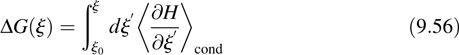
FIGURE 9.8 Illustration of the reaction coordinate in Equation 9.55.
The resulting free energy profile, shown in Figure 9.9, reveals a deep minimum corresponding to the final DA product and a plateau at ξ = 2.75 Å, implying a short-lived intermediate state. If the mechanism were concerted, one would expect a profile with a single minimum, corresponding simply to the final product state. We will see an example of such a profile later when we investigate reactions on the SiC(100)-(2 × 2) surface. The profile in Figure 9.9 is clearly more characteristic of a nonconcerted mechanism involving a well-defined reaction intermediate. That the initial free energy barrier at ξ ≈ 3.25 Å is relatively low (3–4 kcal/mol) suggests that the reaction can occur at room temperature.
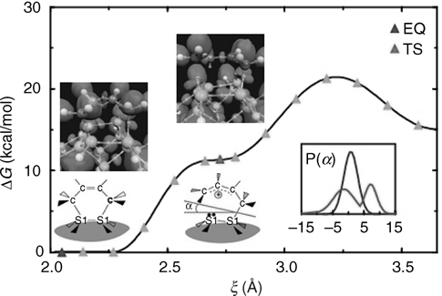
FIGURE 9.9 Free energy along the reaction pathway leading to a Diels–Alder [4+2] adduct. Blue and red triangles indicate the product (EQ) and intermediate states (IS), respectively. Inset shows the buckling angle (α) distribution of the Si dimer for both the IS and the EQ configurations. The snapshots include configurations representing the IS and EQ geometries. Large, medium, and small spheres denote Si, C, and H atoms, respectively, and very small spheres indicate the location of Wannier centers. Darkly shaded spheres locate positively charged atoms. The purple surface is the ELF 0.95 isosurface. A full color version of this figure can be found in Ref. [12].
Note that the barrier to a retro-Diels–Alder reaction, in which the 1,3-butadiene desorbs from the surface is approximately 23 kcal/mol according to the profile in Figure 9.9. This raises an interesting question concerning the use of the chemistry of conjugated dienes on semiconductor surfaces in surface patterning and lithography. In principle, this chemistry has exciting potential applications in this area, however, it has been shown for the [4+2] adduct that the retro-DA process is not observed on Si(100)-(2 × 1). Instead, thermal decomposition was found to be the major reaction pathway upon heating [45]. Assuming that energetic considerations play a major role in the reaction mechanism, one might ask if we can design or “reverse engineer” a chemically substituted diene that would favor a retro-DA reaction over thermal decomposition. Because experiments and static ab initio calculations cannot identify specific mechanisms by which these addition products form, this system is ideal to study using AIMD. Moreover, we will show that AIMD can actually aid in the design strategy.
It is known in organic chemistry that DA reactions increase their rates with increasing strength of the electron-donating groups on the diene. Therefore, it would seem natural to assume that electron-withdrawing groups on the diene have an opposite effect. Furthermore, it can be expected that such groups would destabilize the DA [4+2] adduct, so that it is more likely to undergo a heating induced retro-DA reaction. Based on these ideas, we suggest abutadiene derivative that leads to a lower free energy barrier for the retro-DA reaction. To be considered useful for lithographic purposes, a substituted diene candidate should have the following properties: (i) it should participate in a spontaneous DA [4+2] reaction on the room temperature surface and (ii) the [4+2] adduct should undergo a retro-DA reaction upon heating. In order to account for both requirements, the candidate substituent must have moderate electron-withdrawing ability to favor the retro-DA pathway, while it should also spontaneously react producing the DA [4+2] adduct at a sufficient rate. Based on qualitative arguments, fluorine was chosen as a test substituent, because it is electronegative yet is not considered to be a highly effective electron-withdrawing substituent such as CF3 or SO3H. Specifically, one of the hydrogens on the C = C double bond of the isolated 1,3-butadiene was replaced by F[14]. The substitution is illustrated in Figure 9.10.
The utility of the modified butadiene shown in Figure 9.10 for the retro-DA reaction can be demonstrated by computing the free energy profile for its reaction with the surface and comparing it to that in Figure 9.9. For this calculation, we employ the same protocol as above except that the plane-wave cutoff is increased to 80 Ry because of the highly repulsive pseudopotential needed to describe the fluorine atom. The resulting profile comparison is shown in Figure 9.11. Both profiles show a plateau at the intermediate carbocation state and, therefore, further support the mechanistic picture of Figure 9.7. The figure also shows that, like 1,3-butadiene, 2-F-1,3-butadiene has negligible activation barrier (4–5 kcal/mol) toward the DA [4+2] adduct, so that a spontaneous reaction is expected at room temperature. Although similar in many qualitative aspects, there is a 6–8 kcal/mol decrease in the activation free energy for the retro-DA pathway. The activation energy is still too high for a spontaneous retro-DA reaction upon heating, but this result serves as a proof of concept and illustrates the power of a potential computational engineering principle toward designing functionalizing agents with required chemical characteristics.
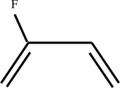
FIGURE 9.10 The 1,3-butadiene derivative 2-F-1,3,butadiene.
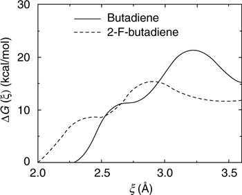
FIGURE 9.11 Free energy along the reaction pathway leading to a Diels--Alder [4+2] adduct. The solid line corresponds to the unmodified 1,3-butadiene, and the dashed line corresponds to the 2-F-1,3-butadiene of Figure 9.10.
9.3.2 Attachment of 1,3-Cyclohexadiene to the Si(100)-(2 × 1) Surface
Since the STM measurements of Ref. [18] were based on 1,3-cyclohexadiene rather than 1,3-butadiene, is it instructive to carry out an analogous set of calculations using the former molecule in order to contrast with the results described in the previous subsection. This system has also been the subject of numerous experimental [1,18,49,58,59] and static ab initio studies [60,63]. Again, however, static calculations cannot reveal mechanistic details or elucidate the role of surface dimer dynamics in the reaction process.
For these calculations, we chose to improve the descriptions of the electronic structure and of the Si(100)-(2 × 1) surface by increasing the size of the periodic slab and by employing the PBE functional rather than the BLYP functional. In these calculations [15], the Kohn–Sham orbitals were expanded in a plane-wave basis with a kinetic energy cutoff of 35 Ry, and Troullier–Martins norm-conserving pseudo-potentials [64], with S, P, and D treated as local for H, C, and Si, respectively, were employed. The Si(100)-(2 × 1) system was comprised of 16 2 × 1 units each five layers deep, with the bottom layer fixed at the bulk lattice positions and terminated with H. The top surface forms two rows of four buckled dimers each. The larger surface dimensions prevents periodic images from interacting with themselves, which eliminates the need for k-point sampling beyond the gamma point. The simulation box dimensions were Lx = 15.47 Å, Ly = 15.5 Å, and Lz = 31.8 Å, where the z-direction is the non periodic direction. Because of the increased system size, a smaller ensemble of trajectories, eleven in total, was generated with the cyclohex-adiene initiated from random configurations 3.0 Å above the surface.
First the cyclohexadiene (CHD) and reconstructed silicon surface were equilibrated separately using Nosé-Hoover chain thermostats [65] at 300K for over 1 ps each to obtain well-thermalized starting configurations. These calculations used a time step of 0.1 fs and a fictitious CP mass of 670 a.u. The final time averaged configurations compared favorably with published experimental structures. All trajectories used the same initial configuration for the CHD and the Si surface but varied in the position and orientation of the CHD. The equilibrated CHD was then placed randomly at 3.0 Å above the equilibrated surface, and in order to maintain adiabaticity for longer periods of time in the combined CHD + Si system, the time step was dropped to 0.05 fs and the fictitious CP mass lowered to 400 a.u. The combined system was then annealed from 0 to 300K under NVE conditions. Next, the center of mass of the CHD was fixed while the system equilibrated for 1 ps using Nosé–Hoover chain thermostats [65] under NVT conditions. Finally, the thermostat and center of mass constraint were removed, and trajectories were run until a reaction product formed or a maximum of 12 ps was reached, after which the trajectory was considered unreactive.
In Figure 9.12, we show the adducts obtained. In particular, we observe four (A, B, Ct, and D) out of the five STM-identified cycloaddition products [18,49] as well as four additional adducts. In contrast to the 1,3-butadiene case, the most probable adduct (C), the [4+2] interdimer, intrarow product, now splits into two isomers that differ in the orientation of the CH2 group. In the previously predicted case, (Ct), the CH2 groups are over the trough, while for the new adduct, (Cr), the CH2 groups are situated over the dimer row. Previous static DFT calculations found that Cr is slightly favored over Ct [62], consistent with the present findings. Experiment is, most likely, unable to distinguish between the two isomers due to the symmetry of the adduct and strong unpaired Si-adduct orbital interactions. Likewise, the [2 + 2] interdimer adduct (E) is oriented such that the π-bond is over the trough, not the dimer row as identified in the STM experiment. However, this adduct may be able to flip orientation to match the experimentally derived structure since the barrier to move the H nearest the Si from the dimer to the trough side of the CHD should be small. In another case, both π-bonds in the CHD reacted to form a 4-bond adduct (F) as was predicted by Lee et al. [66] (labeled 5 in their notation), although the actual mechanism is somewhat different. It should be noted that an H-abstraction from a partially reacted CHD occurred in one of the trajectories. H-abstraction has been observed experimentally between 400 and 700 K [67]. Its presence in our simulation either indicates (1) H-abstraction does occur at lower temperatures, but in such small quantities that it is not detectable experimentally, (2) the extra energy released from the first bond formation created a local hot-spot, or (3) the barriers for H-abstraction are too low within the chosen DFT framework. The percentages of product A, B, Ct, Cr, D, E, and other obtained are 7.1, 7.1, 7.1, 21.4, 28.6, 7.1, and 21.4, respectively [15]. These are to be compared to the experimental populations reported in Table 9.1, however, it must be kept in mind that the ensemble used here is considerably smaller than that used in the butadiene study.
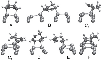
FIGURE 9.12 Snapshots of 1,3-CHD adducts that form on the Si(100)–(2 × 1) surface at 300K. Si, H, and C atoms are large, small, and medium, respectively. The remaining C π-bond are given a darker shading. A full color version of this figure can be found in Ref. [15]. Only the Si dimer and atoms attached to the dimer are shown for clarity. Letters label the various adducts: (A) [4+2] intradimer (Diels–Alder type), (B) [4+2] interdimer across trough, (Ct) [4+2] interdimer same row with CH2 above trough, (Cr) [4+2] interdimer same row with CH2 above row, (D) [2+2] intradimer, (E) [2+2] interdimer, and (F) [4+4] 4-bond.
The reaction mechanism of 1,3-cyclohexadiene is very similar to that observed for 1,3-butadiene. We illustrate this by showing trajectories of the carbon–carbon and carbon–silicon bonds as functions of time for typical trajectories of each of the product states (see Figure 9.13).
As in Figure 9.6, Figure 9.13 shows that the C = C double bonds revert to single bonds at different times during each of the reactions and that the C–Si bonds also form asymmetrically. Thus, we can conclude that both 1,3-cyclohexadiene and 1,3-butadiene react with the Si(100)-(2 × 1) surface via a nonconcerted, asymmetric reaction pathway. This is illustrated in Figure 9.14 for the [4+2] Diels–Alder-like intradimer product. An analysis of the role played by the dimer tilt angle in determining the reaction kinetics reveals that as the molecule approaches the lower, positively charged silicon, the dimer tilt angle decreases somewhat. This is illustrated in Figure 9.15, which shows a plot of tilt angle (ϕ) versus. the carbon–silicon distance (d) for the complete set of trajectories. This figure helps us understand why the Ct and Cr interdimer products are favored: The second attack is more likely to occur on a neighboring dimer because it will generally have a larger tilt angle than the dimer on which the first C–Si bond has already formed and, therefore, its upper silicon will have a larger negative charge (see Figure 9.7 and the ELF plot in Figure 9.16).
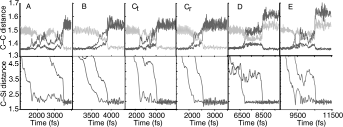
FIGURE 9.13 The top row shows the three possible π-bond lengths averaged over 25 fs for the adducts (see Fig. 9.12) in the reactive region. The bottom row displays the corresponding first and second C–Si bond lengths in light and dark lines, respectively. A full color version of this figure can be found in Ref. [15]. The small figure in A labels the three C–C bonds and the first C–Si bond. The second C–Si would form at positions 1 or 2. All distances given in Å. During the reaction, the C–C and C = C bond lengths fluctuate significantly. After the adduct forms, the remaining π-bond reverts to the original length, while the single C–C bonds are expanded. Change in the π bond lengths coincides with C–Si bond formation.
The longer trajectories and improvement in the electronic structure representation for the 1,3-CHD system allow us to investigate other aspects of the reaction mechanism as well. An important question concerns the possibility of a radical mechanism. Multireference cluster based calculations of the minimum energy pathways for the cycloaddition of CHD to the Si(100)-(2 × 1) surface employing second order perturbation theory [66] suggested that diradical mechanisms should play a major role. Despite experimental evidence to the contrary, [36,68] multi-reference cluster calculations predict that Si surface dimers are symmetric, [42] not tilted, which could alter reaction pathways. As previously noted, periodic DFT calculations performed here capture the correct dimer tilt. At the same time, these calculations neglect surface crossing events since they are single reference.
In order to estimate how important radical mechanisms and surface crossings might be during adduct formation, we have calculated single point energies along four representative trajectories for three spin states: spin restricted (SR), which assumes that all electrons are paired (singlet), spin unrestricted (SU) with the same number of up and down electrons (singlet), and SU with two more up than down electrons (triplet). The SU calculations mimic diradical electronic configurations by allowing up and down electrons to vary spatially to lower the energy. If the up and down electron densities are identical, the SU singlet functional simply reduces to SR. Since DFT is a variational theory, the lowest energy configuration is thermodynamically favorable. Therefore, if the electronic configuration of the lowest energy state changes, the difference between the SR or SU (singlet) and SU (triplet) energies becomes small, and a surface crossing might occur even though it is not allowed within standard DFT.
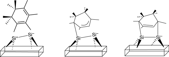
FIGURE 9.14 Schematic representation of the asymmetric, nonconcerted mechanism for the addition of 1,3-cyclohexadiene on the Si(100)-(2 × 1) surface.
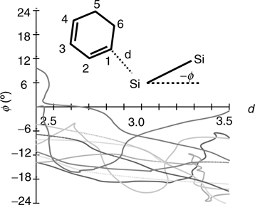
FIGURE 9.15 dC–Si versus. the dimer tilt angle (ϕ). All the dimers are oriented down relative to CHD. Properties in the reactive region immediately prior to the first bond formation. The different shades denote different trajectories. dC–Si is the distance between the C and Si in the first bond. Stars appear at dC–Si = 3.5 Å. A full color version of this figure can be found in Ref. [15].
Figure 9.17 compares the three energies for four representative trajectories. Single point energy calculations were carried out at 0K using configurations taken from the 300K trajectory. In all cases, the SR (black down triangles) and SU singlet (up, light triangles) single point energies were essentially identical (the upper line in the inset shows the energy difference) revealing that spin polarization is not necessary for the singlet case. The SU triplet (light squares) energies are always higher in energy than the SR energies (the lower curve in the inset line is the energy difference), although the difference is sometimes within the error of the calculation as seen in (b) the [4 + 2] interdimer adduct (Ct) and (d) the 4-bond adduct. At no point in (a), the [4 + 2] intradimer adduct, does the triplet state become energetically accessible at 300 K. In (c), the previously unpredicted [4 + 2] interdimer adduct (Cr), only the final adduct, not the transition state, exhibits comparable singlet and triplet energies. Since we are most interested in reaction mechanisms during the adduct formation, the triplet influence should be negligible. We also verified that SR is sufficiently accurate for our system by rerunning a trajectory that formed the (Cr) [4 + 2] interdimer adduct shown in Figure 9.17c using singlet SU. Although there were some variations, the same final adduct formed. Due to the difference between periodic DFT and multireference cluster systems, a definitive statement on the reaction mechanism cannot be made. These calculations do reveal, however, that within periodic GGA DFT, the spin restricted reaction mechanisms studied are favored over the equivalent triplet mechanisms, and hence should play the major role.
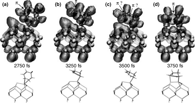
FIGURE 9.16 Two step reaction mechanism for the [4 + 2] intradimer [A] adduct. The ELF is approximately divided between contributions due to CHD (darker surface) and the Si surface (lighter surface). A full color version of this figure can be found in Ref. [15]. Stick figures at the bottom show all bonds, with the π-bonds highlighted in red. The first bond shifts between a “down” Si and (a) the middle of a π-bond or (b) the C closest to the CH2 groups. In (c), the π-bond delocalizes between three adjacent C. Finally (d), the negative “up” Si reacts with the positive C next to the CH2 groups to form the adduct.
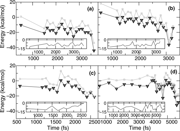
FIGURE 9.17 Comparison of SR (black down triangle), singlet SU (light up triangle), and triplet SU (light squares) OK single point energies (kcal/mol) relative to the isolated CHD and Si(100) surface. Insets show the energy difference (kcal/mol) between SR-singlet SU (upper line) and SR-triplet SU (lower line). A full color version of this figure can be found in Ref. [15]. Representative configurations taken along 300 K trajectories for the (a) [4 + 2] intradimer [A], (b) [4 + 2] interdimer (same row) with CH2 over the trough [Ct], (c) interdimer (same row) with CH2 over the dimer row [Cr], and (d) 4 bond adducts [F]. A singlet radical mechanism is never favorable, although a triplet diradical mechanism may be possible during (b) and (d).
9.4 REACTIONS ON THE SIC(100)-(3 × 2) SURFACE
Silicon carbide (SiC) and its associated reactions with a conjugated diene are interesting surface systems to study and compare to the pure silicon surface case discussed in the preceding section. As we have seen, the Si(100)-(2 × 1) surface allows for a relatively broad distribution of products because the surface dimers are relatively closely spaced. Because of this, creating ordered organic layers on this surface using conjugated dienes seems unlikely unless some method can be found to enhance the population of one of the adducts, rendering the remaining adducts negligible. SiC exhibits a number of complicated surface reconstructions depending on the surface orientation and growth conditions. Some of these reconstructions offer the intriguing possibility of restricting the product distribution due to the fact that carbon–carbon or silicon–silicon dimer spacings are considerably larger.
SiC is often the material of choice for electronic and sensor applications under extreme conditions [69–71] or subject to biocompatibility constraints [72]. Although most reconstructions are still being debated both experimentally and theoretically [73,74], there is widespread agreement on the structure of the 3C-SiC(001)-(3 × 2) surface [75,76] (see Figure 9.18), which will be studied in this section. SiC(001) shares the same zinc blend structure as pure Si(001), but with alternating layers of Si and C. The top three layers are Si, the bottom in bulk-like positions and the top decomposed into an open 2/3 + 1/3 adlayer structure. Si atoms in the bottom two–thirds layers are four-fold coordinated dimers while those Si atoms in the top one-third are asymmetric tilted dimers with dangling bonds. Given the Si-rich surface environment and presence of asymmetric surface dimers, one might expect much of the same Si-based chemistry to occur with two significant differences: (1) altered reactivity due to the surface strain (the SiC lattice constant is ~20% smaller than Si) and (2) suppression of interdimer adducts due to the larger dimer spacing compared to Si (~60% along a dimer row, ~20% across dimer rows). Previous theoretical studies used either static (0 K) DFT calculations of hydrogen, [77–81] a carbon nanotube, [82] or ethylene/acetylene [83,84] adsorbed on SiC(001)-(3 × 2) or employed molecular dynamics of water [85] or small molecules of the CH3-X family [86] on the less thermodynamically stable SiC(001)-(2 × 1) surface. Here, we consider cycloaddition reactions on the SiC-(3 × 2) surface that include dynamic and thermal effects. A primary goal for considering this surface is to determine whether 3C-SiC(001)-(3 × 2) is a promising candidate for creating ordered semiconductor-organic interfaces via cycloaddition reactions.
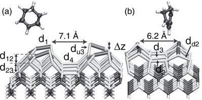
FIGURE 9.18 View of 1,3-CHD + 3C-SiC(001)-(3 × 2) system (a) along dimer rows and (b) between dimers in a row. Si, C, H, and the top Si surface dimers are represented by darker or lighter shading. A full color version of this figure can be found in Ref. [16]. The dimers are spaced farther apart by ~60% along a dimer row and ~20% across dimer rows relative to Si(100)-(2 × 1).
In this study, [16] the KS orbitals were expanded in a plane-wave basis setup to a kinetic energy cutoff of 40 Ry. As in the 1,3-CHD studies described above, exchange and correlation are treated with the spin restricted form of the PBE functional, [24] and core electrons were replaced by Troullier–Martins pseudopotentials [50] with S, P, and D treated as local for H, C, and Si, respectively. The resulting SiC theoretical lattice constant, 4.39 Å, agrees well with the experimental value of 4.36 Å. [76] The full system is shown in Figure 9.18. The 3 × 2 unit cell is doubled in both directions to include four surface dimers to allow the possibility of all interdimer adducts. Again, the resulting large surface area, (18.6 Å × 12.4 Å), allows the Γ-point approximation to be used in lieu of explicit k-point sampling. Two bulk layers of Si and C, terminated by H on the bottom surface, provide a reconstructed (1/3 + 2/3) Si surface in reasonable agreement with experiment (see below). The final system has 182 atoms [24 atoms/layer * (1 Si adlayer + 4 atomic layers) + 2*24 terminating H]. The simulation cell employed lengths of 18.6 Å and 12.4 Å along the periodic directions and 31.2 Å along the nonperiodic z direction.
Both the CHD and SiC(001) surface were equilibrated separately under NVT conditions using Nosé–Hoover chain thermostats [65] at 300 K with a timestep of 0.1 fs for 1 and 3 ps, respectively. When the equilibrated CHD was allowed to react with the equilibrated surface, the time step was reduced to 0.05 fs in order to ensure adiabaticity. The CHD was placed 3 A above the surface, as defined by the lowest point on the CHD and the highest point on the surface. Each of 12 trajectories was initiated from the same CHD and SiC structures but with the CHD placed at a different orientations and/or locations over the surface. The subsequent initialization procedure was identical to the CHD–Si(100) system: First the system was annealed from 0 to 300 K in the NVE ensemble. Following this, it was equilibrated with Nosé–Hoover chain thermostats for 1 ps at 300 K under NVT conditions, keeping the center of mass of the CHD fixed. Finally, the CHD center of mass constraint was removed and the system was allowed to evolve under the NVE ensemble until an adduct formed or 20 ps elapsed.
The reactions that occur on this surface all take place on or in the vicinity of a single surface Si–Si dimer. However, as Figure 9.19 shows, there is not one but rather four adducts that are observed to form. Adduct labels from the Si + CHD study are used for consistency. As postulated, the widely spaced dimers successfully suppressed the interdimer adducts that formed on the Si(100)-(2 × 1) surface [15]. From the 12 trajectories, 3 formed the [4 + 2] Diels–Alder type intradimer adduct (A), 1 produced the [2 + 2] intradimer adduct (D), 5 exhibited hydrogen abstraction (H), and 1 resulted in a novel [4 + 2] subdimer adduct between Si in d1 and d2 (G) (see Figure 9.18). The remaining trajectories only formed 1 C–Si bond within 20 ps. Although the statistics are limited, these results suggest that H abstraction is favorable, consistent with the high reactivity of atomic H observed in experimental studies on this system. [87,88] What is somewhat more troublesome, from the point of view of creating well-ordered organic-semiconducting interfaces is the presence of the subdimer adduct G. All the surface bonds directly connected to the adduct slightly expand to 2.42–2.47 Å, with the exception of one bond to a Si in the third layer, which disappears entirely. The energetic gain of the additional strong C–Si bond outweighs the loss of a strained Si–Si bond. The end effect is the destruction of the perfect surface and the creation of an unsaturated Si in the bulk. One adduct is noticeably missing: the [2 + 2] subdimer adduct. At several points during the simulation this adduct was poised to form but quickly left the vicinity. Most likely, the strain caused by the four-membered ring combined with the two energetically less stable unsaturated Si prevented this adduct from forming, even though the [2 + 2] intradimer and [4 + 2] subdimer adducts are stable.
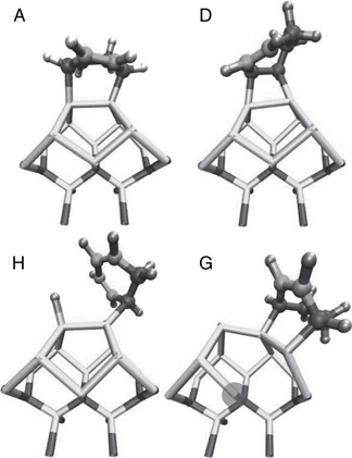
FIGURE 9.19 Snapshots of the four adducts that formed on the SiC surface: (A) [4 + 2] intradimer adduct, (D) [2 + 2] intradimer adduct, (H) hydrogen abstraction, and (G) [4 + 2] subsurface dimer adduct. Si, C, and H are represented by lighter or darker shading, respectively. The remaining C = C bond(s) is more darkly shaded. A full color version of this figure can be found in Ref. [16]. The larger spacing between dimers suppresses interdimer adducts. However, adduct (G) destroys the surface, rendering this system inappropriate for applications requiring well-defined organic-semiconducting interfaces.
In Figure 9.20, we show the carbon–carbon and CHD–Si distances as functions of time for the different adducts observed. This figure reveals that the mechanism of the reactions proceeds in a manner very similar to that of CHD and 1,3-butadiene on the Si(100)-(2 × 1) surface: It is an asymmetric, nonconcerted mechanism that involves a carbocation intermediate. What differs from Si(100) is the time elapsed before the first bond forms and the intermediate lifetime. On the Si(100)-(2 × 1) surface the CHD always found an available “down” Si to form the first bond within less than 10 ps or 40 Å of wandering over the surface. On the SiC(001)-(3 × 2) surface the exploration process sometimes required up to 20 ps and over 100 Å. While the exact numbers are only qualitative, the trend is significant. The Si(100) dimers are more tilted on average, and hence expected to be slightly more reactive. However, the dominant contribution is likely the density of tilted dimers: Si has 0.033 dimers/Å2, but SiC only has 0.017 dimers/Å2. Regardless of whether dimer flipping occurs, it is simply more difficult to find a dimer on the SiC surface.
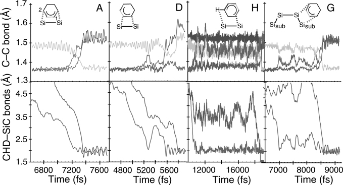
FIGURE 9.20 Relevant bond lengths (Å) versus time (fs) during product formation for four representative adducts. The top row displays the C–C bonds lengths (moving average over 25 fs) while the bottom row plots the first and second CHD – SiC surface bond. The shading follows the same pattern as that of Figure 9.13. A full color version of this figure can be found in Ref. [16]. Change in the C–C bond length closely correlates with surface-adduct bond formation. Intermediate lifetimes over all trajectories range from 0.05 to 18+ ps.
9.5 REACTIONS ON THE SIC(100)-(2 × 2) SURFACE
There is considerable interest in the growth of molecular lines or wires on semiconductor surfaces. Such structures allow molecular scale devices to be constructed using semiconductors such as H-terminated Si(111) and Si(100) or Si(100)-2 × 1 as the preferred substrates. Various molecules can be grown into lines on the H-terminated surfaces, [89] and on the Si(100)-2 × 1 surface, styrene and derivatives such as 2,4-dimethylstyrene or longer chain alkenes can be used to grow wires along the dimer rows. [90–97]. More recently, allylic mercaptan and acetophenone have been shown to grow across dimer rows on the H:Si(100)-(2 × 1) surface. [91,97–100] Other semiconductor surfaces can be considered for such applications, however, these have not received as much attention. An intriguing possible alternate in the silicon–carbide family is the SiC(100)-(2 × 2) surface.
The SiC(100)-(2 × 2) surface exhibits a crucial difference from the SiC(100)-(3 × 2) in that it is characterized by C ≡ C triple bonds, which bridge Si–Si single bonds. These triple bonds are well separated and reactive, suggesting the possibility of restricting the product distribution for the addition of conjugated dienes on this surface. Figure 9.21 shows a snapshot of this surface with a 1,3-cyclohexadiene above it. Previous ab initio calculations suggest that these dimers react favorably with 1,4-cyclohexadiene [101]. Here, we present preliminary results on the free energy profile at 300 K for the reaction of this surface with 1,3-cyclohexadiene, also shown in Figure 9.21. A more detailed study is now available in Ref. [102].
In this study, the KS orbitals were expanded in a plane-wave basis setup to a kinetic energy cutoff of 65 Ry. As in the 1,3-CHD studies described above, exchange and correlation are treated with the spin restricted form of the PBE functional, [24] and core electrons were replaced by Troullier-Martins pseudopotentials [50] with S, P, and D treated as local for H, C, and Si, respectively. The periodic slab contains 128 atoms arranged in six layers (including a bottom passivating hydrogen layer). Proper treatment of surface boundary conditions allowed for a simulation cell with dimensions Lx = 17.56Å, Ly = 8.78 Å, and Lz = 31 Å along the nonperiodic dimension. The surface contains eight C≡C dimers. This setup is capable of reproducing the experimentally observed dimer buckling [103] that static ab initio calculations using cluster models are unable to describe [101].
In Figure 9.22, we show the free energy profile for the [4 + 2] cycloaddition reaction of 1,3-cyclohexadiene with one of the C ≡ C surface dimers. The free energy profile is calculated by dividing the ξ interval ξ ∈ [1.59, 3.69] into 15 equally spaced intervals, and each constrained simulation was equilibrated for 1.0 ps followed by 3.0 ps of averaging using a time step of 0.025 fs. All calculations are carried out in the NVT ensemble at 300 K using Nosé–Hoover chain thermostats [65] In contrast to the free energy profile of Fig. 9.9, the profile in Figure 9.22 shows no evidence of a stable intermediate. Rather, apart from an initial barrier of approximately 8 kcal/mol, the free energy is strictly downhill. The reaction is thermodynamically favored by approximately 48 kcal/mol. The suggestion from Figure 9.22 is that the reaction is symmetric and concerted in contrast to the reactions on the other surfaces we have considered thus far. Figure 9.22 also shows snapshots of the molecule and the surface atoms with which it interacts at various points along the free energy profile. In these snapshots, spheres in the bonds between atoms represent the centers of maximally localized Wannier functions. These provide a visual picture of where new covalent bonds are forming as the reaction coordinate ξ is decreased. By following these, we clearly see that one C – C bond forms before the other, demonstrating the asymmetry of the reaction, which is a result of the buckling of the surface dimers. The buckling gives rise to a charge asymmetry in the C ≡ C surface dimer, and as a result, the first step in the reaction is a nucleophilic attack of one of the C ≡ C bonds in the cyclohexadiene on the positively charged carbon in the surface dimer, this carbon being the lower of the two. Once this first CC bond forms, the second CC bond follows after a change of approximately 0.3 Å in the reaction coordinate with no stable intermediate along the way toward the final [4 + 2] cycloaddition product. In addition, the Wannier centers show the conversion of the triple bond on the surface to a double bond in the final product state.
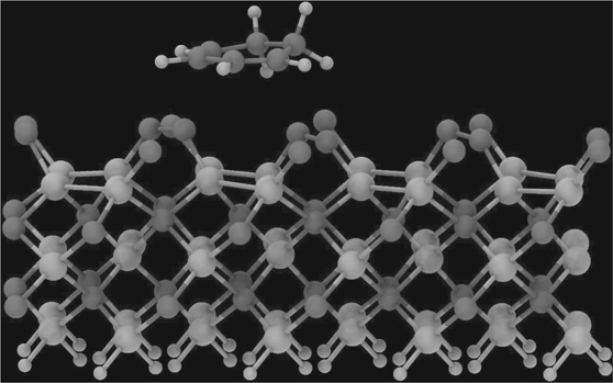
FIGURE 9.21 Snapshot of the SiC-(2 × 2) surface and 1,3-cyclohexadiene molecule. Dark, medium, and lightly shaded spheres represent carbon, silicon, and hydrogen atoms, respectively. A full color version of this figure appears in Ref. [102].
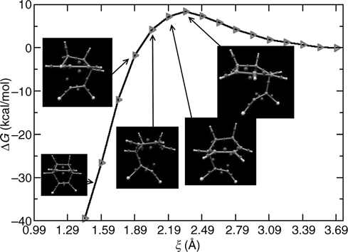
FIGURE 9.22 Free energy profile for the formation of the [4 + 2] Diels–Alder-like adduct between 1,3-cyclohexadiene a C ≡ C dimer on the SiC-(2 × 2) surface. Dark, light, and medium shaded spheres represent C, H, and Si, respectively. Small spheres in the bonds between atoms are the centers of maximally localized Wannier functions. A full color and slightly expanded version of this figure can be found in Ref. [102].
Further evidence for the concerted nature of the reaction is provided in Figure 9.23, which shows the average carbon–carbon lengths computed over the constrained trajectories at each point of the free energy profile. It can be seen that there is a slight tendency for an asymmetric reaction, despite its being concerted.
In order to demonstrate that the [4 + 2] Diels–Alder type cycloaddition product is highly favored over other reaction products on this surface, we show one additional example of a free energy profile, specifically, that for the formation of a [2+2] cycloaddition reaction with a single surface C ≡ C dimer. This profile is shown in Figure 9.24. In contrast to the [4 + 2] Diels–Alder type adduct, the barrier to formation of this adduct is roughly 27 kcal/mol (compared to 8 kcal/mol for the Diels–Alder product). Thus, although the [2 + 2] reaction is thermodynamically favorable, this barrier is sufficiently high that we would expect this particular reaction channel to be highly suppressed compared to one with a 19 kcal/mol lower barrier. The free energy profile, together with the snapshots taken along the reaction path, also suggests that this reaction occurs via an asymmetric, concerted mechanism, as was found for the [4 + 2] Diels–Alder type product.
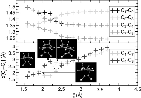
FIGURE 9.23 Average carbon–carbon bond lengths obtained from each constrained simulation. A full color version of this figure can be found in the Supporting Information for Ref. [102].
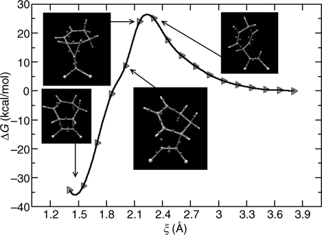
FIGURE 9.24 Free energy profile for the formation of the [2 + 2] adduct between 1,3-cyclohexadiene a C≡C dimer on the SiC-(2 × 2) surface. Dark, light, and medium shaded spheres represent C, H, and Si, respectively. Small spheres in bonds between atoms are the centers of maximally localized Wannier functions. A full color version of this figure can be found in Ref. [102].
Although we have not shown them here, we have computed free energy profiles for a variety of other adducts, [102] including interdimer and sublayer adducts, and in all cases, free energy barriers exceeding 20 kcal/mol (or 40 kcal/mol in the case of the sublayer adduct) were obtained. These results strongly suggest that the product distribution on this surface would, for all intents and purposes, be restricted to the single [4 + 2] Diels–Alder type product, implying that this surface might be a candidate for creating an ordered organic/semiconductor interface. We encourage the reader to visit Ref. [102] for a more detailed version of this study.
9.6 CALCULATION OF STM IMAGES: FAILURE OF PERTURBATIVE TECHNIQUES
Because of the importance of STM techniques in imaging neat as well as functionalized surfaces, it is instructive to comment briefly on the problem of computing such images via density functional approaches. DFT derived STM images have traditionally been calculated by two methods: Tersoff–Hamann [104] and Bardeen perturbation theory [105]. Several excellent reviews of DFT-derived STM methods exist in the literature [106,107]. Tersoff–Hamann, the simplest approximation, assumes that the tunneling current is proportional to the electron density above the surface:
![]()
where ψν (r) is the νth wave function of the sample with energy Eν, rtip is the location of the probe, and EF is the Fermi energy of the sample. Bardeen perturbation theory [105] adds an additional level of complexity by explicitly including the contributions of the tip from a separate DFT calculation, with the current given by
![]()
Here f (E) is the Fermi function, V is the applied voltage, Eμ and Eν are tip and sample energy levels, and Mμν is the tunneling matrix element between tip and surface states ψμ and ψν, respectively.
In either case, it is assumed that the tip does not alter the geometry or the electronic structure of the surface. Once the DFT-derived Kohn–Sham energies and wave functions for the tip and surface are in hand, the STM image over a range of bias and isocurrents can be calculated using the same data set. In this section, we employ an STM code developed by Kováĉik and Marx [108,109] based on the Bardeen perturbation theory implementation given by Hofer et al. [106]. The spatial resolution of the calculated STM images is 0.14 Å.
In order to investigate the applicability of perturbative schemes, we return to the 1,3-CHD/Si(100)-(2 × 1) system considered earlier. The DFT implementation employed in this section is that in the Quantum Espresso code [110]. The KS orbitals are expanded in a plane waves are expanded up to 36 Ry and exchange correlation is treated at the LDA level [111]. The Kleinman–Bylander [64] pseudopotential forms are employed. During 0 K geometry optimizations, the total force on each atom is reduced to less than 1.0 × 10⁻³ a.u.
The tip is taken to be a tungsten tip, for which separate DFT calculations are required in order to apply the Bardeen perturbation theory. Six electrons are included for each W atom. The W(110) bcc tip is comprised of three pyramidal layers on two (2 × 3) bulk layers fixed at the theoretically derived lattice constant (3.12 Å) with Lz = 26.9 Å. The three pyramidal layers and any adatom on the apex of the tip (Si or O) are allowed to fully relax. Combined tip–surface calculations fix the lateral dimensions at the bulk Si value (15.5 Å × 15.5 Å) and expand Lz to 34.8 Å. The expanded lateral dimensions require (3 × 5) W-bulk layers (30 atoms/layer), resulting in a minimum bulk W strain of (0.9% × 16.8%). In order to maintain the integrity of the tip crystalline structure, all of the tip must be fixed at scaled ideal coordinates except for the z-component of the three pyramidal layers. Representative finite temperature and ideal clusters are extracted from the corresponding full surface configurations by taking the positions of the CHD and nearest 10 Si and terminating all 12 broken bonds with H. In all cases, the large unit cell allowed the gamma point approximation to be employed.
Teague and Boland [18,49] characterized at least five types of CHD adducts on the Si(100)-(2 × 1) surface by identifying unpaired Si dimers and π* orbitals on the C = C bond through empty-state STM imaging. We focus here on the [4 + 2] intradimer CHD adduct for simplicity, but similar results hold for the other adducts. Figure 9.25 shows a representative set of images computed over an AIMD trajectory of 3.5 ps. The images appear to match closely those reported by Teague and Boland, [18] but they match for the wrong reasons. Superimposing the Si surface dimers and CHD adduct on top of the isosurface reveals that the even through the Si-dimers are correctly described, the dumbbell-like protrusions correspond to the CH2 groups, not the C = C bond! Adding impurities to the tip is not sufficient to resolve this problem [17].
However, if we compute forces in all three spatial directions (two parallel to the surface and one perpendicular) due to the STM tip (see Figures 9.26 and 9.27 for an illustration of the system setup and the forces in the three spatial directions exerted on the molecule by the tip), we find that the tip exerts a strong attractive force on the C = C bond in agreement with recent experiments, [59] but it also exerts a strong repulsive force on the CH2 groups, and these various perturbations change the molecular geometry as well as the energetic ordering of the virtual orbitals [17]. These forces are large enough that perturbative techniques cannot be reliably applied to compute images of covalently bound floppy molecules.
FIGURE 9.25 Representative STM images computed within the Bardeen formalism for Vsurf = 0.2 V and isocurrent I = 1.0 × 10⁻¹⁰ A at different time points along a 3.5 ps trajectory. The last panel on the right is the thermal averaged image over the trajectory. A full color version of these images can be found in Ref. [17].
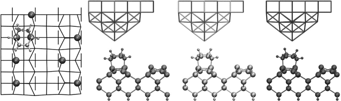
FIGURE 9.26 W (110) tip over the [4 + 2] intradimer cyclohexadiene (CHD) adduct adsorbed on the Si(100) reconstructed surface. The geometry optimized tip is initially placed 3.0 Å vertically (relative to the C = C midpoint) above the independently optimized CHD at the left C in CH2 (left), midpoint of CH2–CH2 bond (middle), and right C in CH2 (right) as marked by the red, orange, and blue dots, respectively, in the far left sketch. The dark spheres highlight which Si are at least the same height as the Si connected to CHD. A full color version of this figure can be found in Ref. [17].
Given the failures of perturbative methods, we suggest [17] employing the NEGF formalism [112–114] to compute STM images. NEGF methods, which include tip–surface interactions in the calculated I-V curve, can circumvent the problems with perturbative methods encountered above. They do so, however, at a substantial increase in computational overhead, particularly for empty-state imaging. In a NEGF
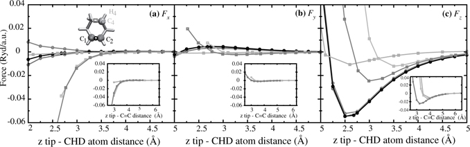
FIGURE 9.27 Tip - CHD z-distance versus (a) x-, (b) y-, and (c) z-force (Ryd/au) when the W(110) tip is positioned either over C1 (light), C1 = C2 midpoint (darkest), C2 (next lightest), H4 (next lightest), C4 (lightest), and CH2 -CH2 midpoint. Each DFT calculation uses the structure from separate geometry optimized Si(100) surface + CHD and W(110) + W bulk calculations. The insets show the same data, but with the corresponding tip-C = C midpoint z-distance. In (a) there is a strong drive to push the CH2 groups away from the tip. A full color version of this figure can be found in Ref. [17].
calculation, the current is computed according to
![]()
where G = [E − H0 + eV − Σ(E)]−1 is the Green's function at energy E, the Hamiltonian H0 includes the molecule, the STM tip, and the surface region near the molecule treated atomistically. f1(E) and f2(E) are the Fermi functions of the tip and surface, respectively, and Γ1 (E) and Γ2 (E) are related to the imaginary part of the self-energy operators (Σ(E)) of the tip and surface, respectively. The latter treat the coupling of the atoms included explicitly in H0 to the extended external environment. Since the tip perturbs both the wave function and geometry as a function of the relative tip–surface position, separate NEGF calculations must be done at each point instead of treating the tip and surface separately once and for all. If each NEGF calculation were inexpensive, then generating a 3D map in order to extract a fixed height or isocurrent image would be tedious, but not prohibitive. In practice, each individual calculation is costly using standard methods, and the development of more efficient self-consistent techniques based on the NEGF approach remains an outstanding challenge.
REFERENCES
1. Filler, M. A.; Bent, S. F. Prog. Surf. Sci. 2002, 73, 1–56.
2. Kachian, J. S.; Wong, K. T.; Bent, S. F. Acc. Chem. Res. 2010, 43, 346–355.
3. Basu, R.; Kinser, C. R.; Tovar, J. D.; Hersam, M. C. Chem. Phys. 2006, 326, 144–150.
4. Pitters, J. L.; Dogel, I.; DiLabio, G. A.; Wolkow, R. A. J. Phys. Chem. B 2006, 110, 2159–2163.
5. Hossain, M. Z.; Kato, H. S.; Kawai, M. J. Am. Chem. Soc. 2005, 127, 15030–15031.
6. Kirczenow, G.; Piva, P. G.; Wolkow, R. A. Phys. Rev. B 2005, 72, 245306.
7. Lopinski, G. P.; Wayner, D. D. M.; Wolkow, R. A. Nature 2000, 406, 48–51.
8. Car, R.; Parrinello, M. Phys. Rev. Lett. 1985, 55, 2471–2474.
9. Marx, D.; Hutter, J. Modern methods and algorithms of quantum chemistry. In Grotendorst, J., Ed. Ab Initio Molecular Dynamics: Theory and Implementations. Fz Juelich, NIC, 2000, pp. 301–449.
10. Tuckerman, M. E. J. Phys.:Condens. Matter 2002, 14, R1297–R1355.
11. Marx, D.; Hutter, J. Ab Initio Molecular Dynamics. Cambridge University Press, Cambridge, 2009.
12. Minary, P.; Tuckerman, M. E. J. Am. Chem. Soc. 2004, 126, 13920–13921.
13. Minary, P.; Tuckerman, M. E. J. Am. Chem. Soc. 2005, 127, 1110–1111.
14. Iftimie, R.; Minary, P.; Tuckerman, M. E. P. Natl. Acad. Sci. U.S.A. 2005, 102, 6654–6659.
15. Hayes, R. L.; Tuckerman, M. E. J. Am. Chem. Soc. 2007, 129, 12172–12180.
16. Hayes, R. L.; Tuckerman, M. E. J. Phys. Chem. C 2008, 112, 5880–5887.
17. Hayes, R. L.; Tuckerman, M. E. J. Phys. Chem. C 2010, 114, 15102.
18. Teague, L. C.; Boland, J. J. J. Phys. Chem. B 2003, 107, 3820–3823.
19. Tuckerman, M. E.; Yarne, D. A.; Samuelson, S. O.; Hughes, A. L.; Martyna, G. J. Comput. Phys. Commun. 2000, 128, 333–376.
20. Kohn, W.; Sham, L. J. Phys. Rev. A 1965, 140, 1133–1138.
21. Hohenberg, P.; Kohn, W. Phys. Rev. B 1964, 136, 864–871.
22. Becke, A. D. Phys. Rev. A 1988, 38, 3098–3100.
23. Lee, C.; Yang, W.; Parr, R. G. Phys. Rev. B 1988, 37, 785–789.
24. Perdew, J. P.; Burke, K.; Ernzerhof, M. Phys. Rev. Lett. 1996, 77, 3865–3868.
25. Marx, D.; Tuckerman, M.; Martyna, G. Comp. Phys. Commun. 1999, 118, 166–184.
26. Tuckerman, M. E.; Parrinello, M. J. Chem. Phys. 1994, 101, 1302–1315.
27. Tuckerman, M. E.; Martyna, G. J. J. Chem. Phys. 1999, 110, 2810–2821.
28. Minary, P.; Tuckerman, M. E.; Pihakari, K. A.; Martyna, G. J. J. Chem. Phys. 2002, 116, 5351–5362.
29. Minary, P.; Morrone, J. A.; Yarne, D. A.; Tuckerman, M. E.; Martyna, G. J. J. Chem. Phys. 2004, 121, 11949–11956.
30. Resta, R.; Sorella, S. Phys. Rev. Lett. 1999, 82, 370–373.
31. Berghold, G.; Mundy, C. J.; Romero, A. H.; Hutter, J.; Parrinello, M. Phys. Rev. B 2000, 61, 10040–10048.
32. Thomas, J. W.; Iftimie, R.; Tuckerman, M. E. Phys. Rev. B 2004, 69, 125105.
33. Iftimie, R.; Thomas, J. W.; Tuckerman, M. E. J. Chem. Phys. 2004, 120, 2169.
34. Sharma, M.; Wu, Y. D.; Car, R. Intl. J. Quant. Chem. 2003, 95, 821.
35. Becke, A. D.; Edgecombe, K. E. J. Chem. Phys. 1990, 92, 5397.
36. Over, H.; Wasserfall, J.; Ranke, W.; Ambiatello, C.; Sawitzki, R.; Wolf, D.; Moritz, W. Phys. Rev. B 1997, 55, 4731–4736.
37. Ono, M.; Kamoshida, A.; Matsuura, E.; Ishikawa, T. E.; Hasegawa, Y. Phys. Rev. B 2003, 67, 201306.
38. Takagi, N.; Shimonaka, S.; Aruga, T.; Nishijima, M. Phys. Rev. B 1999, 60, 10919–10925.
39. Stoll, E. P.; Baratoff, A.; Mangili, A.; Maric, D. Mater. Sci. Eng. 1996, B37, 155–157.
40. Weakliem, P. C.; Smith, G. W.; Carter, E. A. Surf. Sci. 1990, 232, L219–L223.
41. Gryko, J.; Allen, R. E. Ultramicroscopy 1992, 42–44, 793–800.
42. Olson, R. M.; Gordon, M. S. J. Chem. Phys. 2006, 124, 081105.
43. Madelung, O. Data in Science and Technology—Semiconductors: Group IV Elements and III–V Compounds. Springer-Verlag; 1991.
44. Teplyakov, A. V.; Kong, M. J.; Bent, S. F. J. Am. Chem. Soc. 1997, 119, 11100–11101.
45. Teplyakov, A. V.; Kong, M. J.; Bent, S. F. J. Chem. Phys. 1998, 108, 4599–4606.
46. Hovis, J. S.; Liu, J. S.; Hamers, R. J. J. Phys. Chem. B 1998, 102, 6873–6879.
47. Mui, C.; Bent, S. F.; Musgrave, C. B. J. Phys. Chem. A 2000, 104, 2457–2462.
48. Bent, S. F. Surf. Sci. 2003, 500, 879–903.
49. Teague, L. C.; Boland, J. J. Thin Solid Films 2004, 464–465, 1–4.
50. Troullier, N.; Martins, J. L. Phys. Rev. B 1991, 43, 1993–2006.
51. Brewer, L. Lawrence Berkeley Laboratory Report 1977, LBL–3720.
52. Yin, M. T.; Cohen, M. L. Phys. Rev. B 1980, 24, 2303.
53. Minary, P.; Martyna, G. J.; Tuckerman, M. E. J. Chem. Phys. 2003, 118, 2527–2538.
54. Yoshinobu, J.; Yamashita, Y.; Yasui, F.; Mukai, K.; Tsuneyuki, S.; Akagi, K.; Hamaguchi, K.; Machida, S.; Nagao, M.; Sato, T.; Iwatsuki, M. J. Electron. Spectrosc. Relat. Phenom. 2001, 114–116, 383–387.
55. Jones, M., Jr. Organic Chemistry. W. W. Norton and Co, New York, 2005.
56. Carter, E. A.; Ciccotti, G.; Hynes, J. T.; Kapral, R. Chem. Phys. Lett. 1989, 156, 472.
57. Sprik, M.; Ciccotti, G. J. Chem. Phys. 1998, 109, 7737.
58. Naydenov, B.; Ryan, P.; Teague, L. C.; Boland, J. J. Phys. Rev. Lett. 2006, 97, 098304.
59. Naydenov, B.; Teague, L. C.; Ryan, P. M.; Boland, J. J. Nano Lett. 2006, 6, 1752–1756.
60. Konecny, R.; Doren, D. J. J. Am. Chem. Soc. 1997, 119, 11098–11099.
61. Choi, C. H.; Gordon, M. S. J. Am. Chem. Soc. 1999, 121, 11311–11317.
62. Teague, L. C.; Chen, D.; Boland, J. J. J. Phys. Chem. B 2004, 108, 7827–7830.
63. Galperin, M.; Beratan, D. N. J. Phys. Chem. B 2005, 109, 1473–1480.
64. Kleinman, L.; Bylander, D. M. Phys. Rev. Lett. 1982, 48, 1425.
65. Martyna, G. J.; Klein, M. L.; Tuckerman, M. E. J. Chem. Phys. 1992, 97, 2635–2643.
66. Lee, H. S.; Choi, C. H.; Gordon, M. S. J. Am. Chem. Soc. 2005, 127, 8485–8491.
67. Kong, M. J.; Teplyakov, A. V.; Jagmohan, J.; Lyubovitsky, J. G.; Mui, C.; Bent, S. F. J. Phys. Chem. B 2000, 104, 3000–30007.
68. Mizuno, S.; Shirasawa, T.; Shiraishi, Y.; Tochihara, H. Phys. Rev. B 2004, 69, 241306.
69. Capano, R. J.; Trew, R. J. MRS Bull. 1997, 22, 19.
70. Starke, U. Silicon Carbide: Fundamental Questions and Applications to Current Device Technology. Springer-Verlag, Berlin, Germany, 2004.
71. Melinon, P.; Masenelli, B.; Tournus, F.; Perez, A. Nat. Mater. 2007, 6, 479–490.
72. Stutzmann, M.; Garrido, J. A.; Eickhoff, M.; Brandt, M. S. Phys. Stat. Sol. A 2006, 203, 3424–3437.
73. Soukiassian, P. G.; Enriquez, H. B. J. Phys.:Condens. Matter 2004, 16, S1611–S1658.
74. Pollmann, J.; Kriiger, P. J. Phys.:Condens. Matter 2004, 16, S1659–S1703.
75. D'angelo, M.; Enriquez, H.; Aristov, V. Y.; Soukiassian, P.; Renaud, G.; Barbier, A.; Noblet, M.; Chiang, S.; Semond, F. Phys. Rev. B 2003, 68, 165321.
76. Tejeda, A.; Dunham, D.; García de Abajo, F. J.; Denlinger, J. D.; Rotenberg, E.; Michel, E. G.; Soukiassian, P. Phys. Rev. B 2004, 70, 045317.
77. Di Felice, R.; Bertoni, C. M.; Pignedoli, C. A.; Catellani, A. Phys. Rev. Lett. 2005, 94, 116103.
78. Peng, X.; Kriiger, P.; Pollmann, J. Phys. Rev. B 2005, 72, 245320.
79. Chang, H.; Wu, J.; Gu, B.-L.; Liu, F.; Duan, W. Phys. Rev. Lett. 2005, 95, 196803.
80. Peng, X.; Kriiger, P.; Pollmann, J. Phys. Rev. B 2007, 75, 073409.
81. Peng, X.; Kriiger, P.; Pollmann, Phys. Rev. B 2007, 76, 125303.
82. de Brito Mota, F.; de Castilho, C. M. C. Phys. Rev. B 2006, 74, 165408.
83. Wieferink, J.; Kriiger, P.; Pollmann, J. Phys. Rev. B 2006, 74, 205311.
84. Wieferink, J.; Kriiger, P.; Pollmann, J. Phys. Rev. B 2007, 75, 153305.
85. Cicero, G.; Catellani, A.; Galli, G. Phys. Rev. Lett. 2004, 93, 016102.
86. Cicero, G.; Catellani, A. J. Chem. Phys. 2005, 122, 214716.
87. Amy, F.; Chabal, Y. J. J. Chem. Phys. 2003, 119, 6201–6209.
88. Derycke, V.; Soukiassian, P. G.; Amy, F.; Chabal, Y.; D'Angelo, M. D.; Enriquez, H. B.; Silly, M. G. Nat. Mater. 2003, 2, 253–254.
89. McNab, I. R.; Polanyi, J. C. Chem. Rev. 2006, 106, 4321.
90. DiLabio, G. A.; Piva, P. G.; Kruse, P.; Wolkow, R. A. J. Am. Chem. Soc. 2004, 126, 16048.
91. Hossain, M. Z.; Kato, H. S.; Kawai, M. J. Phys. Chem. B 2005, 109, 23129.
92. Hossain, M. Z.; Kato, H. S.; Kawai, M. J. Am. Chem. Soc. 2005, 127, 15030.
93. DiLabio, G. A.; Dogel, S. A.; Anagaw, A.; Pitters, J. L.; Wolkow, R. A. Phys. Chem. Chem. Phys. 2007, 9, 1629.
94. Hossain, M. Z.; Kato, H. S.; Kawai, M. J. Am. Chem. Soc. 2007, 129, 3328.
95. Hossain, M. Z.; Kato, H. S.; Kawai, M. J. Am. Chem. Soc. 2007, 129, 12304.
96. Zikovsky, J.; Dogel, S. A.; Haider, A. B.; DiLabio, G. A.; Wolkow, R. A. J. Phys. Chem. A 2007, 111, 12257.
97. Hossain, M. Z.; Kato, H. S.; Kawai, M. J. Am. Chem. Soc. 2008, 130, 11518.
98. Hossain, M. Z.; Kato, H. S.; Kawai, M. J. Phys. Chem. C 2009, 113, 10751.
99. Ferguson, G. A.; Than, C. T. L.; Raghavachari, K. J. Phys. Chem. C 2009, 113, 11817.
100. Ferguson, G. A.; Than, C. T. L.; Raghavachari, K. J. Phys. Chem. C 2010, 1, 679.
101. Bermudez, V. M. Surf. Sci. 2003, 540, 255–264.
102. Zhang, Y. and Tuckerman, M. E. J. Phys. Chem. Lett. 2011, 2, 1814–1819.
103. Derycke, V.; Soukiassian, P.; Mayne, A.; Dujardin, G. Surf. Sci. 2000, 446, L101–L107.
104. Tersoff, J.; Hamann, D. R. Phys. Rev. B 1985, 31, 805–813.
105. Bardeen, J. Phys. Rev. Lett. 1961, 6, 57–59.
106. Hofer, W. A.; Foster, A. S.; Shluger, A. L. Rev. Mod. Phys. 2003, 75, 1287–1331.
107. Gottlieb, A. D.; Wesoloski, L. Nanotechnology 2006, 17, R57–R65.
108. Kovacik, R.; Meyer, B.; Marx, D. Angew. Chem. Int. Ed. 2007, 46, 4894–4897.
109. Kovacik, R. Characterization of Catalyst Surfaces by Ab Initio Thermodynamics and STM Data Calculations. Thesis, Ruhr-Universitat Bochum, 2007.
110. Baroni, S.; Dal Corso, A.; de Gironcoli, S.; Giannozzi, P.; Cavazzoni, C.; Ballabio, G.; Scandolo, S.; Chiarotti, G.; Focher, P.; Pasquarello, A.; Laasonen, K.; Trave, A.; Car, R.; Marzari, N.; Kokalj, A. Quantum Espresso Package, http://www.pwscf.org/, 2008.
111. Ceperley, D. M.; Alder, B. J. Phys. Rev. Lett. 1980, 45, 566–569.
112. Keldysh, L. V. Sov. Phys. JETP 1965, 20, 1018.
113. Calzolari, A.; Marzari, N.; Souza, I.; Nardelli, M. B. Phys. Rev. B 2004, 69, 035108.
114. Datta, S. Nanotechnology. 2004, 15, S433.
Functionalization of Semiconductor Surfaces, First Edition
Edited by Franklin (Feng) Tao and Steven L. Bernasek.
© 2012 John Wiley & Sons, Inc. Published 2012 by John Wiley & Sons, Inc.