
CHAPTER 1
Introduction
FRANKLIN (FENG) TAO, YUAN ZHU, AND STEVEN L. BERNASEK
1.1 MOTIVATION FOR A BOOK ON FUNCTIONALIZATION OF SEMICONDUCTOR SURFACES
Microelectronics has grown into the heart of modern industries, driving almost all the technologies of today. Semiconductor materials play ubiquitous and irreplaceable roles in the development of microelectronic computing, micro- and optoelectronic devices, microelectromechanical machines, three-dimensional memory chips, and sensitive silicon-based nano- or biological sensors. Being the most technologically important material, silicon and its surface chemistry have received phenomenal attention in the past two decades. One important motivation for semiconductor surface chemistry is to fine-tune the electronic properties of device surfaces and interfaces for applications in several technologically important areas. Chemical attachment of molecules to the semiconductor surface enables the necessary control over electron transfer through the semiconductor–organic interface. It also allows control of the architecture of the organic overlayer by chemical modification of the functionalized silicon-based templates. It provides a versatile and reproducible way to tailor the electronic properties of semiconductor surfaces in a controllable manner.
Organic molecules are widely used in areas from plastics to semiconductors. Compared to the world of inorganic materials, organic materials exhibit unique chemical and physical properties and biocompatibility. In addition, the availability of an enormous number of organic materials with a large number of different functional groups offers opportunity for tuning physical and chemical properties that is absent for inorganic materials. A few examples are organic semiconducting polymer materials including organic electroluminescent and organic light emitting diodes. The advantage of organic materials has driven the interest in incorporation of functional organic materials, such as size and shape effects, absorption spectrum, flexibility, conductivity, chemical affinity, chirality, and molecular recognition into existing silicon-based devices and technologies. Dry organic reactions in vacuum and wet organic chemistry in solution on 2D templates are the two major approaches for functionalization of these surfaces.
Functionalization of semiconductor surfaces has also been driven by significant technological requirements in several areas, including micro- and nanoscale electromechanical devices and new nanopatterning techniques. By combining molecular surface modification and nanofabrication of semiconductor materials and surfaces, selective functionalization on nanopatches and formation of organic nanostructures become quite important for nanopatterning of organic materials for application in devices. The development of these heterogeneous structures requires mechanistic understanding of organic modification at the nano- and even atomic scale.
These applications in several areas have driven the enormous efforts in functionalization of semiconductor surfaces with organic materials and the subsequent immobilization of biospecies at the surface in the past two decades. Significant achievements have resulted from these efforts. Reaction mechanisms of many organic molecules have been studied at the molecular level. Numerous organic monolayers have been grown. Furthermore, organic multilayer architectures have been developed as well. Incorporation of functional biospecies such as DNA has been demonstrated and prototype biosensor devices have been made. In light of these achievements in the past two decades, a book summarizing this progress and pointing the direction for future work in this area would certainly be useful.
1.2 SURFACE SCIENCE AS THE FOUNDATION OF THE FUNCTIONALIZATION OF SEMICONDUCTOR SURFACES
1.2.1 Brief Description of the Development of Surface Science
Historically, surface science has been developed since the spontaneous spreading of oil on water was studied by Benjamin Franklin [1]. From the 1900s to 1950s, surface science studies focused on the properties of chemisorbed monolayers, adsorption isotherms, molecular adsorption and dissociation, and energy exchange [2]. As surface science became important for understanding production processes in industries such as pretreatment, activation, poisoning, and deactivation of catalysts in production, it has become one of the major areas of chemistry and physics.
In the 1950s, surface science experienced an explosive growth driven by the advance of vacuum (UHV) technology and the availability of solid-state device-based electronics with acceptable cost [3]. Thus, many efforts were made in the study of surface structure and chemistry since clean single-crystal surfaces could be prepared in UHV at that time. In the 1960s, the advance of surface analytical techniques resulted in a remarkable development of surface science. Many surface phenomena such as adsorption, bonding, oxidation, and catalysis were studied at the atomic and molecular level.
In the 1980s, the invention of various scanning probe microscopes greatly accelerated the development of surface science [4], giving rise to a second explosive growth of surface science. These probing techniques make it possible to study surfaces and interfaces at the atomic level. Particularly important, these techniques allow scientists to actually visualize surfaces at the atomic level and to identify geometric structure and electronic structure of surfaces at the highest resolution. This breakthrough radically changed the scientists' vision of the properties of materials, from average information at a large scale to local information at the atomic scale. Numerous surface phenomena were reexamined at the atomic level. For example, scanning tunneling microscopy provided an opportunity to visualize atoms on various surfaces of metals and semiconductors [5,6]. Atomic level information achieved with these techniques significantly aided in the identification of specific sites of catalytic reactions [7,8]. In addition, the breakthrough in surface analytical techniques expanded the territory of surface science to almost all areas of materials science, physics, chemistry, and mechanical and electronic engineering. More importantly, semiconductor and microelectronic industries have largely benefited from the advancement of surface science [9–13] since all the protocols for the fabrication of semiconductor devices and microelectronic components extensively involve surface science and vacuum technology.
In recent years, the development of biochemistry and biomolecular engineering has given surface science another opportunity [14,15]. Surface science studies of various bioprocesses and biofunctions performed in nature largely rely on an understanding of the complicated liquid–liquid, liquid–solid, and liquid–gas interfacial phenomena in these biosystems. For example, the functions of some biospecies largely depend on the self-assembly of specific biomolecules at interfaces in nature. The functions and behaviors of some biospecies can be mimicked on a 2D chip toward the development of biosensing technology, which extensively involves interfacial chemistry. The terms “biosurface” and “biointerface” have been widely used to describe these studies.
1.2.2 Importance of Surface Science
The term “surface science” often makes people instantly have a connection to various surface analytical techniques used in their research fields of chemistry, materials science, and physics. It is true that the development of surface science has significantly relied on the invention and advance of new analytical techniques capable of providing different information at surfaces and interfaces [1,16]. In fact, every aspect of our daily life and work involves surface science. Most of the production processes in chemical industries involve catalytic reactions performed at the interface between solid catalysts at high temperature and gaseous phases under high pressure or liquid reactants with high flow rate. New energy conversion processes extensively involve heterogeneous catalysis such as (1) evolution of H2 and O2 on the surfaces of cocatalysts in solar-driven water splitting [17–22] and (2) generation of electricity from oxidation of fuel molecules on the surface of electrodes (Pt or Pt-based alloy) in fuel cells [23–25]. Most issues in environmental science involve chemical process occurring on the surface of various materials such as minerals under ambient conditions [26–28]. For example, chemical conversion of greenhouse gases to fuel and conversion of toxic emissions are typically heterogeneous processes occurring on specific catalysts [29,30].
The surface chemistry of semiconductors is essentially the core of the field of functionalization of semiconductor surfaces. This is because all the processes to functionalize the inorganic surface with organic molecules must be performed as interfacial reactions. In fact, the functions and behaviors of organic layers/devices developed on semiconductor surfaces are truly determined by the surface structure and reactive site of the semiconductor, the reactivity and selectivity of the organic molecules, and the binding strength of semiconductor–organic linkages such as Si–X (X=C, O, N, S,…). Thus, the fundamental studies of surface science in this field are crucial, which is abundantly demonstrated in the following chapters.
1.2.3 Chemistry at the Interface of Two Phases
Typically, the interactions at two different phases can be categorized into noncovalent weak interactions and covalent binding. Corresponding to this categorization, strategies used in the design of new materials and devices can be categorized as (1) molecular self-assembly through weak noncovalent forces and (2) breaking of chemical bonds and the formation of new ones [10,31,32]. The macroscopic self-assembled structure formed on a substrate is typically held together by various weak noncovalent forces between adsorbed molecules within a self-assembled structure and between the adsorbed molecules and template (Fig. 1.1). In this case, the ordered supramolecular systems with new structures and properties form spontaneously from the original components. By using weak noncovalent binding including electrostatic interactions between static molecular charges, hydrogen bonding, van der Waals forces, π–π interactions, hydrophilic binding, and charge transfer interactions, many new self-assembled structures with various sizes, shapes, and functions have been produced [10,31,32].
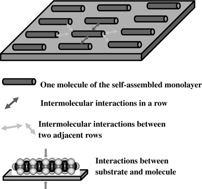
FIGURE 1.1 Schematic of a self-assembled monolayer on solid surfaces.
In contrast to weak interactions in these systems, strong chemical bonding is commonly existent in many interfacial materials such as semiconductor surface materials and devices functionalized with organic molecules [10,31,33]. A large number of surface technologies rely on strong chemical binding at interfaces. For example, surface etching, chemisorption, and thin film growth strongly depend on the formation of chemical bonds at interfaces.
Other than the strong chemical binding and weak van der Waals interaction, chemical adsorption of molecules on metal surfaces in heterogeneous catalysis can be considered as the third type of interaction [2,16,34]. The strength of this type of interaction is between the weak van der Waals and the strong chemical binding (mostly covalent binding). Such binding with a medium strength is, in fact, necessary for heterogeneous catalysis since (1) binding of reactant molecules with certain strength results in a residence time for reactant molecules on the surface of the catalysts and the attainment of a certain coverage, and may aid in bond breaking in some cases, and (2) a strong binding will decrease molecular mobility on surfaces to some extent, which is necessary in producing intermediates or the final product molecules.
Regarding the functionalization of semiconductor surfaces for the preparation of new semiconductor devices, biosensors, molecular electronic devices, and nano-patterning templates, a strong and highly selective binding of organic molecules or biospecies is actually necessary. In most cases, the binding between the organic molecule and the semiconductor surface is covalent bonding instead of van der Waals forces.
1.2.4 Surface Science at the Nanoscale
Surface science has been studied at nanoscale well before the “nano” term was frequently used. Surface processes are performed at the nanoscale though the size of a surface could be as large as centimeter or more. In fact, the information volume along the surface normal is in the range of nanometers, since interaction at the interface is performed only in the surface region with a thickness of a few atomic layers, which is distinctly different from homogeneous process of organic reactions occurring in solution. In addition, STM has revealed that actually most samples are heterogeneous in lateral dimensions. Typically, a uniform surface feature is identified only at tens of nanometers. Thus, surface processes do occur at the nanoscale though the size of the material is macroscopic. For a crystallite with a size less than 100 nm such as 0D, 1D, 2D, and 3D nanomaterials, certainly the surface chemistry on these materials is already at the nanoscale. Overall, studies of chemistry on the surface at the nanoscale are important for understanding chemical and physical properties of solid surfaces. Thus, we term the surface chemistry on nanomaterials or nanoscale domain on the surface of materials with macroscopic size as nanoscale surface science.
For surfaces with different size at the nanoscale, there are size-dependent surface structural features. For example, as schematically shown in Fig. 1.2, fractions of atoms at the edge of the surface increases with a decrease in size of the surface domain. This is also true for atoms at the metal–oxide interface (Fig. 1.3). More importantly, these size-dependent geometric structural factors can induce size-dependent electronic factors, surface chemistry, and functions of surfaces. The increased fraction of atoms on the surface results in large surface free energy. Chemical binding of organic molecules on these atoms at the edge of surface domains with low coordination numbers (Fig. 1.2) could be quite different from those at the center of surface domains. In addition, the packing of atoms on the surface and in surface region of nanomaterials could not follow the crystallographic periodicity of atomic packing of materials with a macroscopic size, which suggests different surface chemistry at the nanoscale in contrast to that on large domains and crystallites. Thus, size matters in surface chemistry of organic molecules on semiconductor surfaces.
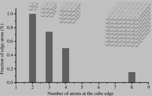
FIGURE 1.2 Fraction of atoms at edge and corner of nanoparticles with different size.
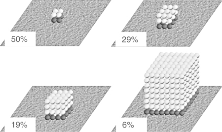
FIGURE 1.3 The size-dependent metal—oxide, per text interfacial area of catalysts. The atoms at the interface are highlighted in gray and the fractions of the interface atoms are shown at the corner of each model.
1.2.5 Surface Chemistry in the Functionalization of Semiconductor Surfaces
Chemical attachment of organic molecules to form organic thin films on different substrates is an important strategy for modification of chemical and physical properties of solid surfaces. Organic attachment is one of the main approaches to the functionalization of solid surfaces since the properties and functions of the attached organic layers are generally absent for inorganic substrates. More importantly, this organic modification and functionalization allows surface and interfacial properties to be tailored controllably since a myriad of organic molecules are available and the structure and property of organic materials can be systematically varied.
The surface and interfacial chemistry involved in the properties of semiconductor surfaces modified with organic molecules/biospecies includes surface structure, binding configuration, orientation of molecules, reaction mechanisms of organic molecules on those surfaces, and their connection to the function and behavior of the modified surfaces. Properties such as conductivity, surface polarity, friction, and biocompatibility can be modified and controlled by this functionalization.
Thus, all the aspects of functionalization of semiconductor surfaces indeed start from the fundamental surface chemistry of the semiconductor surface. From the point of view of information volume, it is at the nanoscale. In terms of reaction sites, most of the surfaces offer different reaction sites at the nanoscale. Thus, it is necessary to identify reaction details at the nanoscale. Overall, due to the nature of the heterogeneity of the functionalized surface, the understanding of surface chemistry in functionalization of semiconductor surface at the nanoscale is necessary.
1.3 ORGANIZATION OF THIS BOOK
The functionalization of semiconductor surfaces originated with fundamental studies of semiconductor surfaces at the atomic level for the successful development of semiconductor-based devices. This book covers (1) the early fundamental studies of semiconductor surface structure and the origin of surface reactive sites by using various vacuum-based surface analytical techniques, (2) creative and systematic studies of surface reactions of various organic molecules and the mechanistic understanding of reactions at semiconductor–organic interfaces at the atomic level, (3) chemical attachment of organic molecules and the formation of organic monolayers to template multilayer organic architectures on semiconductor surfaces, and (4) further functionalization of semiconductor surfaces by chemical reactions between biocompatible functional groups of organic layers and biospecies.
Characterization of the functionalized semiconductor surfaces at the molecular and atomic scales involves several techniques of spectroscopy and microscopy. The major surface science techniques will be briefly introduced in Chapter 2. Substrates used in these functionalization are typically Si(100), Si(111)-(7×7), Ge(100), and diamond(100) in the route of dry functionalization. Functionalization through wet chemistry uses hydrogenated or halogenated semiconductor surfaces (Si–H, Ge–H, Si–X, or Ge–X). Surface structure of these substrates and the origin of their reactive sites will be reviewed in Chapter 3.
The functionalization of semiconductor surfaces through dry chemistry and wet chemistry is the process that occurs at the organic molecule–semiconductor interface. Most of the chemical binding involved in these processes is strong covalent binding with a strength of 20–50 kcal/mol. The reaction mechanisms in the functionalization of these semiconductor surfaces are quite diverse because of the availability of reactive sites with different geometric and electronic structures and thus different reactivity toward organic molecules and definitely numerous organic materials with different functionalities. Significant efforts have been made in the understanding of these reaction mechanisms at the organic–silicon interface. Chapters 4, 5, 6, 7, 8 will review the main studies in terms of reaction mechanisms and summarize reaction mechanisms involved in most of the functionalization of semiconductor surfaces through dry chemistry. Chapter 9 reviews extensive theoretical studies of the mechanisms of organic functionalization of semiconductor surfaces. Focusing on the reaction of conjugated dienes on the semiconductor surface, insights into the reaction mechanisms and dynamics are provided.
As briefly introduced in Section 1.2.5, surface reactions are essentially performed at the nanoscale. The reaction at interfaces occurs on specific surface sites at the nanoscale. Characterization of these sites is an important component in mechanistic studies of reactions leading to the functionalization of semiconductor surfaces. One of the most important techniques to explore nanoscale surface chemistry is STM. Other than the basic function of imaging surface structure at the atomic level, STM has been used to create surface sites and further induce surface reaction of organic molecules for functionalization of semiconductor surfaces and formation of nano-patterns of organic molecules. In fact, tip-induced organic reaction can be considered as a separate strategy for functionalization of semiconductor surfaces. Chapter 10 will describe the function of STM in nanoscale surface chemistry toward functionalization of semiconductor surfaces.
Organic reactions on semiconductor surfaces performed in solution (wet chemistry) provide another important strategy for functionalization of semiconductor surfaces. These protocols and reaction mechanisms will be reviewed in Chapters 11 and 12.
Chapter 13 will summarize the applications of semiconductor surface tethered with organic molecules to the development of biosensing techniques. For example, growth of a multilayer thin film with a tunable thickness will possibly provide a flexible modification for the electronic properties of semiconductor-based devices, including electron transfer efficiency. In addition, multilayer architecture with outward facing functional groups, acting as a tether for a biospecies, is extremely important for designing biosensors. A change in physical properties such as tunneling current or fluorescence can be used to monitor the specific bioresponse. By identifying the change in physical signal induced by the binding of biospecies on the organic functionalized semiconductor surfaces, new diagnostic methods and biomedical sensing technologies can be developed.
The last chapter provides a perspective for the field of functionalization of semiconductor surfaces in the near future. It is possible to study the evolution of the surface chemistry of functionalized surfaces under reactive conditions such as in O2 and humid environment at relatively high temperatures since in situ techniques such as ambient pressure XPS are available. Further research into the reaction mechanisms of immobilization of organic multilayer architectures and biospecies will be carried out. In addition, the incorporation of metal or semiconductor nanoparticles through organic reactions between the tethered functional groups of semiconductor surfaces and the end group of capping agents of nanoparticles is likely since such immobilization can bring unique physical and chemical properties into the field of functionalization of semiconductor surfaces.
REFERENCES
1. Franklin, B. Philos. Trans. R. Soc. Lond. 1774, 64, 445.
2. Somorjai, G. A.; Li, Y. Introduction to Surface Chemistry and Catalysis, 2nd ed. Wiley, Hoboken, NJ, 2010.
3. Ertl, G.; Freund, H.-J. Phys. Today 1999, 52 (1), 32.
4. Binnig, G.; Rohrer, H.; Gerber, C.; Weibel, E. Phys. Rev. Lett. 1982, 49 (1), 57.
5. Besenbacher, F.; Lauritsen, J. V.; Linderoth, T. R.; Laegsgaard, E.; Vang, R. T.; Wendt, S. Surf. Sci. 2009, 603 (10–12), 1315.
6. Vang, R. T.; Lauritsen, J. V.; Laegsgaard, E.; Besenbacher, F. Chem. Soc. Rev. 2008, 37 (10), 2191.
7. Otero, R.; Rosei, F.; Besenbacher, F. Annu. Rev. Phys. Chem. 2006, 57, 497.
8. Lauritsen, J. V.; Besenbacher, F. In Advances in Catalysis, Vol. 50 Academic Press, New York, 2006, p. 97.
9. Neergaard Waltenburg, H.; Yates, J. T. Chem. Rev. 1995, 95 (5), 1589.
10. Tao, F.; Bernasek, S. L.; Xu, G.-Q. Chem. Rev. 2009, 109 (9), 3991.
11. Stiévenard, D.; Legrand, B. Prog. Surf. Sci. 2006, 81 (2–3), 112.
12. Filler, M. A.; Bent, S. F. Prog. Surf. Sci. 2003, 73 (1–3), 1.
13. Wolkow, R. A. Annu. Rev. Phys. Chem. 1999, 50 (1), 413.
14. Demers, L. M.; Ginger, D. S.; Park, S.-J.; Li, Z.; Chung, S.-W.; Mirkin, C. A. Science 2002 296 (5574), 1836.
15. Taton, T. A.; Mirkin, C. A.; Letsinger, R. L. Science 2000 289 (5485), 1757.
16. Ertl, G.; Knozinger, H.; Weitkamp, J. Handbook of Heterogeneous Catalysis. Wiley-VCH, 2008.
17. Kamat, P. V. J. Phys. Chem. Lett. 2009, 1 (2), 520.
18. Kamat, P. V. J. Phys. Chem. C 2008, 112 (48), 18737.
19. Kamat, P. V. J. Phys. Chem. C 2007, 111 (7), 2834.
20. Chakrapani, V.; Tvrdy, K.; Kamat, P. V. J. Am. Chem. Soc. 2010, 132 (4), 1228.
21. Farrow, B.; Kamat, P. V. J. Am. Chem. Soc. 2009, 131 (31), 11124.
22. Maeda, K.; Domen, K. Chem. Mater. 2009, 22 (3), 612.
23. Adzic, R.; Zhang, J.; Sasaki, K.; Vukmirovic, M.; Shao, M.; Wang, J.; Nilekar, A.; Mavrikakis, M.; Valerio, J.; Uribe, F. Top. Catal. 2007, 46 (3), 249.
24. Shao-Horn, Y.; Sheng, W.; Chen, S.; Ferreira, P.; Holby, E.; Morgan, D. Top. Catal. 2007, 46 (3), 285.
25. Bing, Y. H.; Liu, H. S.; Zhang, L.; Ghosh, D.; Zhang, J. J. Chem. Soc. Rev. 2010, 39 (6), 2184.
26. Centi, G.; Ciambelli, P.; Perathoner, S.; Russo, P. Catal. Today 2002, 75 (1–4), 3.
27. Oberdorster, G.; Oberdorster, E.; Oberdorster, J. Environ. Health Perspect. 2005, 113 (7), 823.
28. Weiss, W.; Ranke, W. Prog. Surf. Sci. 2002, 70 (1–3), 1.
29. Liu, X. M.; Lu, G. Q.; Yan, Z. F.; Beltramini, J. Ind. Eng. Chem. Res. 2003, 42 (25), 6518.
30. Bowker, M. Chem. Soc. Rev. 2008, 37 (10), 2204.
31. Tao, F.; Bernasek, S. L. Chem. Rev. 2007, 107 (5), 1408.
32. Love, J. C.; Estroff, L. A.; Kriebel, J. K.; Nuzzo, R. G.; Whitesides, G. M. Chem. Rev. 2005, 105 (4), 1103.
33. Ma, Z.; Zaera, F. Surf. Sci. Rep. 2006, 61 (5), 229.
34. Ertl, G. Reactions at Solid Surface. Wiley, 2009.
Functionalization of Semiconductor Surfaces, First Edition.
Edited by Franklin (Feng) Tao and Steven L. Bernasek.
© 2012 John Wiley & Sons, Inc. Published 2012 by John Wiley & Sons, Inc.