
CHAPTER 3
Structures of Semiconductor Surfaces and Origins of Surface Reactivity with Organic Molecules
YONGQUAN QU AND KELI HAN
In recent years, the interface of semiconductor materials has been a subject of intensive studies. Achieving rationally designed semiconductor surfaces with controllable configurations and special properties benefits the further applications of devices and lithography at the atomic level. Thus, various investigations have been performed to study the surface reactivity of organic molecules on semiconductor surfaces. Especially, single crystalline Si(100), Ge(100), Si(111), and diamond(100) are of particular interest. In this chapter, the surface structures and reactivity of the four semiconductor surfaces will be discussed.
3.1 INTRODUCTION
The chemistry of organic molecules on semiconductor surfaces has attracted much attention and has become a central issue in the field of surface chemistry [1–12]. Interaction between semiconductor surfaces and organic molecules is expected to be a crucial step toward applications in the areas of hybrid organic-semiconductor devices, biological devices, and nanolithography [1–12]. Many organic molecules, such as ketones, amino acids, nitrile compounds, and aromatic compounds, have been investigated to elucidate the mechanism of surface reactions between organic molecules and semiconductor surfaces. Investigations have shown that organic molecules containing more than one functional group cannot create a high degree of order at the semiconductor surface because of competitive reactions between different functional groups of the molecule and the semiconductor surface. Therefore, nonselective bonding at the semiconductor surfaces is observed. Fundamental understanding of the attachment chemistry of organic molecules at semiconductor surfaces and controllable surface modification are still a challenging topic in the functionalization of semiconductor surfaces.
Studying the interaction between molecules and semiconductor surfaces also elucidates the oxidation, reduction, doping and etching mechanisms of semiconductor materials [2,11–13]. For example, the interactions between halogens and silicon are vital in understanding the semiconductor etching process, as well as the deposition process using chorine-containing precursor such as SiH2Cl2. Understanding the interaction between oxygen with semiconductor surfaces will unveil the mechanism of the oxidation process of semiconductor materials, and may further improve the performance of electronic devices. Understanding surface reactions between semiconductor surfaces and etchants will help optimize the etching conditions and improve etching selectivity of different semiconductor materials or different orientations of the same semiconductor materials. Furthermore, understanding the surface of semiconductor materials also will aid the investigation of epitaxial growth on semiconductor surfaces by chemical vapor deposition (CVD) methods. For example, the interaction of disilane (Si2H6) with Si(100) has been widely studied as a model system for understanding the chemical vapor deposition growth process.
Semiconductor surfaces that have garnered particular interest are Si(100), Ge(100), diamond(100), and Si(111). The reactivity of clean semiconductor surfaces and hydrogen- or halogen-terminated semiconductor surfaces differ because of their surface geometry and electronic structures. In order to explain and predict the selectivity of multifunctional organic molecules adsorbed on semiconductor surfaces and to control the oxidation, reduction, doping and etching processes in the current semiconductor industry, it is extremely important to understand the surface electronic structures and reactivity of semiconductors. The interactions of various organic molecules with Si(100), Ge(100), diamond(100) and Si(111) surfaces have been well reviewed [1–12]. This significant requirement has been stimulated by the development of technologies with atomic resolution such as scanning tunneling microscopy (STM), high-resolution electron energy loss spectroscopy (HREELS), synchrotron radiation (SR), and low energy electron diffraction (LEED). With the invention of the STM technology in the early 1980s [14,15], it has been become possible to directly observe the surface structure and electronic properties of semiconductor materials at the atomic level. Herein, we summarize the structures and preparation methods of single crystal semiconductor surfaces including clean Si(100), Si(111)-(7×7), Ge(100), and diamond(100) for dry organic reactions in vacuum and hydrogen/halogen-terminated semiconductor surfaces for wet chemistry. The reactive sites and activity of these semiconductor surfaces for organic functionalization will also be discussed.
3.2 GEOMETRY, ELECTRONIC STRUCTURE, AND REACTIVITY OF CLEAN SEMICONDUCTOR SURFACES
Clean semiconductor surfaces are generally prepared by annealing substrates under ultrahigh vacuum (UHV) at high temperature, followed by a sputtering process with Ar+ ions to remove surface contamination such as adsorbed molecules, oxides and carbides. A slow cooling down process induces surface reconstruction of the semiconductor material. Surface structures are sensitive to vacuum. The cleanest silicon surface is obtained with around 1% defects if the initial background pressure is held within the range of 10−9−10−11 Torr [1].
3.2.1 Si(100)-(2×1), Ge(100)-(2×1), and Diamond(100)-(2×1) Surfaces
Silicon is a group IV semiconductor with a bulk crystal structure known as the diamond structure, which consists of atoms with a coordination number of four in a tetrahedral geometry as shown in Fig. 3.1a [4]. Truncation of a bulk diamond structure along the (100) direction cuts through two Si–Si bonds for each surface silicon atom and leaves surface atoms with two covalent bonds to the bulk and two dangling bonds with one electron in each. Clearly, such a structure is thermodynamically unstable and the clean surface of Si(100) will undergo surface reconstruction to achieve a lower energy state. The earliest proposed surface reconstruction of Si(100)-(2×1) was a simple lateral translation, in which two adjacent surface silicon atoms pair together, forming a surface dimer as shown in Fig. 3.1b [16]. Although a number of alternative surface reconstruction models of Si(100) have been proposed [17,18], theoretical calculations indicate that the most thermodynamically stable surface structure is the formation of dimers [19–21]. Lately, Si(100)-(2×1) reconstruction was finally confirmed on the basis of STM studies carried out by Hamers et al. [22–24]. Fig. 3.2 shows STM images of highly ordered surface silicon dimers for both filled and empty states. Filled and empty states were controlled by STM tip bias.
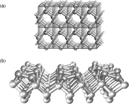
FIGURE 3.1 Surface structure of the clean Si(100) surface. (a) Bulk diamond structure of crystalline silicon. Each atom is tetrahedrally bonded to four neighboring atoms. (b) Surface structure of Si(100) surface after (2×1) reconstruction. The dimer rows are spaced by trenches. Reprinted with permission from Ref. 4. Copyright 2003 Elsevier Ltd.
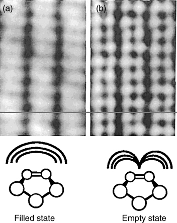
FIGURE 3.2 STM images of clean Si(001) surface probing the filled surface states and empty surface states: (a) Vsample = −2.0 V and (b) Vsample = 2.3 V. Itunnel = 0.2 nA; dimensions=23 Å × 77 Å. Reprinted with permission from Ref. 12. Copyright 1996 American Chemical Society.
Due to the solid-state electronic effects, the surface dimers tilt out of the surface plane. However, STM measurements at room temperature have observed nontilted surface dimers as the major surface structure as shown in Fig. 3.2 [22–24]. The tilted dimers are typically observed near edges or defects due to the break of intrinsic symmetry [22–24]. A model was proposed to explain this conflict between STM measurements and structural calculations. The surface dimers are tilted, but flipping back and forth between two tilt directions due to thermal excitation [22]. STM measurements confirm that silicon dimers are asymmetrically tilted at low temperature (120K) while measurements at room temperature display symmetric dimers [25]. Molecular dynamics simulations confirm this finding and demonstrate that silicon dimers dynamically tilt on the picosecond timescale at room temperature [26]. If the tilting of dimers is alternative between dimer rows, a c(4×2) structure can observed. Otherwise, a p(2×2) structure will be formed on the clean silicon surface. Previous LEED studies showed the c(4×2) structure, indicating an alternating arrangement of the surface dimers [27].
Fig. 3.3 shows the reactive site types of the reconstructed Si(100)-(2×1) surface. Each surface dimer contains a strong σ-bond and a weak π-bond, as shown in Fig. 3.3a. The reported values of this weak π-bond energy is approximately 2–8 kcal/mol [28–33], which is far less that the 64kcal/mol of traditional alkenes [34]. This surface dimer with a strong σ-bond and a weak π-bond still can show similar chemical reactivity with alkenes from classic organic chemistry and lead to pericyclic reactions on Si(100)-(2×1) surfaces. Another character of the reconstructed Si(100)-(2×1) surface is thermodynamically tilted dimers. Electronic charge is transferred from a recessed silicon atom or “down atom” to the protruding, or “up atom,” as shown in Fig. 3.3b, resulting in the electrophilic down silicon atom and the nucleophilic up silicon atom for a surface dimer. The charge separation between the nucleophilic and electrophilic dimer atoms adds zwitterionic character to the surface dimers [35], leading to the observation of nucleophilic–electrophilic reactions. Numerous experiments and calculations have indicated that surface reactions could happen across several rows or on several surface dimers of a row, which depends on the size of organic molecules and total energy after surface adsorption. Fig. 3.3c1–c4 shows the possible reactive sites for disigma binding between Si(100)-(2×1) surfaces and adsorbents on the same dimer (Fig. 3.3c1), two adjacent surface dimers of the same row (Fig. 3.3c2), or two surface dimers of two adjacent rows (Fig. 3c3–c4). The possible tetrasigma binding reactive sites are shown in Fig. 3.3d1 and d2.
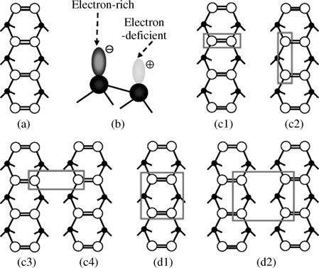
FIGURE 3.3 Surface structure and reactive sites of Si(100)-(2×1) reconstructed surfaces. (a) Top view of dimer and dimer row. (b) Electron transfer and distribution of buckled-down and buckled-up silicon atoms of a Si=Si dimer. (c1), (c2), (c3), and (c4) are disigma binding sites. (d1) and (d2) are tetrasigma binding sites. Reprinted with permission from Ref. 8. Copyright 2009 American Chemical Society.
Clean Ge(100) surfaces show surface (2×1) reconstruction, similar to that of the clean Si(100) surface. Thus, Ge(100)-(2×1) surfaces also show reactivity to many organic molecules due to their surface dimer characterization. Compared to Si(100)-(2×1) surfaces, Ge(100)-(2×1) surfaces exhibit statically tilted dimers at both low temperature and higher temperature [36]. Clean diamond(100) surfaces show similar surface reconstruction with a (2×1) geometry. However, the surface dimers of diamond(100) surfaces remain symmetric, leading to different chemistry activity compared to those of clean Si and Ge(100) surfaces [9,37].
Reactivity of various molecules on semiconductor surfaces is contingent on the electronic structure and geometry of the semiconductor surfaces. Cycloaddition reactions are discussed as an example to illustrate the relationship between reactivity and surface structures. Experiments indicate that cycloaddition reactions happen on the Si(100)-(2×1) surface in a surprisingly facile pathway. In contrast, the reactivity on clean Ge(100)-(2×1) and diamond(100)-(2×1) surfaces are quite low. The reactivity of [2+2] cycloaddition of cyclopentene on Si(100)-(2×1) is ca. 10 times faster than that on Ge(100)-(2×1) surface [37]. The same reaction on diamond(100)-(2×1) surfaces is barely observed. These dramatically different results could be attributed to the surface electronic structures of the three semiconductor surfaces. In classic organic chemistry, the [2+2] C=C cycloaddition reaction is kinetically forbidden and strongly depends on the π–π* splitting of the reactants [38]. The values of π–π* surface-state band gaps are 110 kJ/mol [39], 140 kJ/mol [40], and 350kJ/mol [41] for Si(100)-(2×1), Ge(100)-(2×1), and diamond(100)-(2×1) surfaces, respectively. Therefore, based on these values, the highest reactivity for the [2+2] cycloaddition reactions on the Si(100)-(2×1) surface can be predicted. Experiments also confirm this trend of reactivity. The difference of reactivity on these three semiconductor surfaces can be explained by the unique geometry of the surface dimers, which may play a critical role in controlling surface reactivity. The tilted dimers on Si(100)-(2×1) and Ge(100)-(2×1) surfaces show an asymmetric character, lowering the energy barrier for [2+2] cycloaddition reactions [4,11]. Ab initio theoretical calculations also show [2+2] cycloaddition reactions on Si(100)-(2×1) and Ge(100)-(2×1) surfaces go through low barriers via such a tilted surface structure. The absence of a tilted dimer structure on diamond(100)-(2×1) surfaces is largely responsible for its low [2+2] cycloaddition reaction rate [37,42,43]. Additionally, molecules absorbed on Ge(100)-(2×1) surfaces can be desorbed at elevated temperatures [44]. In contrast, the absorbed molecules on Si(100)-(2×1) surfaces are much more stable. This could be attributed the Si–C bond, which is much stronger than the Ge–C bond. Theoretical calculations indicate that the Si–C bond is stronger than the Ge–C bond by 8.9 kcal/mol for 1,3-butadiene on Si(100)-(2×1) and Ge(100)-(2×1) surfaces [42].
[4+2] cycloaddition reactions are kinetically favorable for all semiconductor surfaces. Reactivity of [4+2] cycloaddition on semiconductor surfaces is similar to that of [2+2] cycloaddition. Notably, adsorption of a diene-like molecule on semiconductor surfaces shows the structure of [4+2] cycloadditions are much more stable than those of [2+2] cycloaddition. Considering the dissociated and formed bonds for both reactions, the stability of the products is mainly determined by the surface stabilization energy. The four-membered ring structures formed in [2+2] cycloadditions show much higher strain than six-membered ring structures from [4+2] cycloaddition reactions. However, adsorption of dienes on Si(100)-(2×1) and Ge(100)-(2×1) surfaces leads to nonselective surface binding due to the low energy barriers for both [2+2] and [4+2] cycloaddition [37,42].
Another type of reaction is nucleophilic/electrophilic reaction of the Si(100)-(2×1) and Ge(100)-(2×1) surfaces due to the tilted surface dimers. The “down” surface atom (electron deficient) can react with a nucleophile to form a dative bond [45–49]. The “up” surface atom also can donate its electron density to a molecule containing an electron deficient center and form a dative bond [50]. Certain functional groups, including amino, phosphine, alcohol, carbonyl, and nitrile, can form dative bonds with the surface dimers [4]. The strength of the dative bonds is determined by the electronegativity of the atoms involved in the formation of the dative bond and the hybridization. Due to close values of electronegativity of Si(1.9) and Ge(2.01), experiments and calculations have demonstrated that the Si(100)-(2×1) and Ge(100)-(2×1) surfaces do not differ significantly in the formation of dative bonds for the same molecules [4].
3.2.2 Si(111)-(7×7) Surface
Reconstruction of Si(111) surfaces has been widely studied through various experimental techniques and theoretical calculations. The current accepted model is dimer-adatom-stacking (DAS) fault model proposed by Takayanagi et al. [51]. This structure is formed through a complicated layer-by-layer reconstruction on a base layer with 49 silicon atoms of the (111) surface, which reduces the number of 3-coordinated Si atoms from 49 to 19 in each unit cell. A top view of a 7×7 unit cell is schematically presented in Fig. 3.4a. Fig. 3.4b1 and b2 shows the unoccupied and occupied state STM images of a clean Si(111)-(7×7) surface, respectively. The 19 dangling bonds are located at 7 spatially inequivalent types of Si atoms, namely, corner and center adatoms on both faulted and unfaulted halves, faulted and unfaulted rest atoms, and the corner-hole atom. Upon reconstruction, each rest atom or corner atom has a formal charge of −1, while each adatom has electron occupancy of only 5/12, leading to a formal charge of approximately +7/12. Furthermore, each center adatom has two neighboring rest atoms, but only one for each corner adatom. The amount of charge transferred from a center adatom to the rest atom is roughly twice as much as that from a corner adatom. Consequently, the corner adatom has a higher electron density of occupied states than the center adatom, implying their different reactivities. The inherent differences in the electron structure among these atoms are readily distinguishable in the STM images. It is evident that this surface provides a number of spatially and electronically inequivalent reactive sites. Because of the large difference in electron density among surface atoms containing dangling bonds, an adatom coupled with one adjacent rest atom can act as a strong dipole, making addition reactions of alkenes with Si(111)-(7×7) possible, similar to the polar additions of unsaturated organic molecules with Si(100) [6–8]. For convenience, the reaction involving one C=C bond is termed as [2+2]-like addition. Similarly, if a conjugated diene participates, it is called [4+2]-like addition.
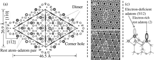
FIGURE 3.4 Surface structure and reactive sites of Si(111)-(7×7). (a) Top view of a reconstructed 7×7 unit cell. (b1) STM images of unoccupied states of a clean Si(111)-(7×7) surface. (b2) STM images of occupied states of a clean Si(111)-(7×7) surface. (c) Electronic transfer and distribution of the reactive site, a pair of adatoms, and its adjacent rest atom. Reprinted with permission from Ref. 8. Copyright 2009 American Chemical Society.
3.3 GEOMETRY AND ELECTRONIC STRUCTURE OF H-TERMINATED SEMICONDUCTOR SURFACES
Hydrogenation of semiconductor surfaces changes the chemical and physical properties of semiconductors. Hydrogenation will remove surface dangling bonds of clean semiconductor surfaces, resulting in low reactivity. Hydrogenation will change surface states of semiconductor surfaces and, thus, change the physical properties of the semiconductor. For example, a clean diamond surface is an insulator, while H-terminated diamond is a p-type semiconductor [52]. There are many applications for H-terminated semiconductor surfaces including nanolithography and molecular electronic devices [1]. To obtain controllable H-terminated semiconductor surfaces will be a key issue for future applications. In this section, the preparation of H-terminated semiconductor surfaces and structures will be discussed. There are three general methods to create H-terminated semiconductor surfaces: (1) hydrogenation under UHV with hydrogen atoms; (2) hydrogenation by chemical methods; and (3) hydrogen plasmas.
3.3.1 Preparation and Structure of H-Terminated Semiconductor Surfaces Under UHV
This method is the most common method of preparation for H-terminated semiconductor surfaces. The interaction between clean semiconductor surfaces and hydrogen molecules is extremely weak because of the high bond energy of hydrogen. A hot tungsten filament is used to generate hydrogen atoms by thermal decomposition of hydrogen molecules under UHV conditions [53–55]. The method is a simple and a general method for creating H-terminated Si(100)-(2×1), Ge(100)-(2×1) and Si (111)-(7×7) surfaces. Adjustable experimental parameters that will affect the structures of the semiconductor surfaces include temperature of the tungsten filament, temperature of the semiconductor surface, distance between the filament and sample, and pressure of hydrogen in the chamber at the time of deposition [1,8]. The surface structures and formation of hydrides on the H-terminated semiconductor surfaces can be determined by STM, RHEED, and HREELS. Complete hydrogenation can be achieved by the above method. Herein, H-terminated Si(100)-(2×1) surfaces will be discussed as a model system for study of the hydrogenation process. STM studies indicate that there are three structures for absorbed hydrogen including monohydride, hemihydride, and ordered (3×1) structures as shown in Fig. 3.5 [56].
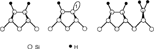
FIGURE 3.5 Structural model of hydrogen on Si(001), showing monohydride, hemihydride, and (3×1) structures. Reprinted with permission from Ref. 12. Copyright 1996 American Chemical Society.
The common structure of H-Si(100) surfaces is the monohydride, in which hydrogen atoms bond to each end of the dimers. At lower coverage, it is possible to form hemihydride structures, in which only one hydrogen bonds to one atom of the dimers and leaves one dangling bond with one electron [56]. However, the hemihydride structure is less stable than the monohydride structure. This is easily understood after considering the energies of formation of each structure during absorption. Adsorption of two hydrogen atoms on same dimer silicon atoms only breaks one surface dimer, leading to the formation of monohydride. In contrast, the formation of hemihydride for two hydrogen atoms on the surface requires the breaking of two surface dimers. Therefore, it is thermodynamically favorable for H atoms to pair onto a single silicon dimer. All theoretical calculations support such a behavior. Boland performed an STM study that confirmed that there was a strong tendency for H atoms to bond onto the same dimer even at low coverage [54,55,57]. At coverage greater than one monolayer, it is possible to form an ordered (3×1) structure containing monohydride units with dihydride (SiH2) groups as shown in Fig. 3.5 [56]. The high H exposure results in a disordered mixture of monohydride, dihydride, and trihydride [56].
3.3.2 Preparation and Structure of H-Terminated Semiconductor Surfaces in Solution
H-terminated semiconductor surfaces also can be prepared through wet chemistry methods. Clean silicon or germanium substrates with a layer of native oxide are immersed into dilute HF or NH4F solution to remove native oxide and subsequently form H-terminated surfaces [58–60]. The surface smoothness can be identified by the sharpness of vibrational peaks of ν(Si-H) stretch at ~2080cm−1 or the ν(Ge-H) stretch at ~2100cm−1 [59]. Multiple hydrides, such as SiH, SiH2, and SiH3, can be formed by adjusting reaction conditions. Treatment of crystal silicon(100) wafers with dilute (1–2%) aqueous HF yields the dihydride SiH2 surface with roughness on the nanometer scale [61]. Atomically flat surfaces with monohydride SiH termination can be achieved through treatment of commercial Si(111) orientation with degassed 40% aqueous NH4F [62].
3.3.3 Preparation and Structure of H-Terminated Semiconductor Surfaces Through Hydrogen Plasma Treatment
The H-diamond(100) surface cannot be obtained by thermal cracking of hydrogen molecules and, therefore, is H-terminated via hydrogen plasma. Microwave heating of hydrogen gas at a relatively high pressure generates a hydrogen plasma that is in contact with the sample surfaces for hydrogenation [63]. Hydrogen plasma plays three roles during the process, including removal of surface roughness, etching of surface graphite-like carbon, and hydrogenation. The surface of H-terminated diamond(100) is stable in air for several weeks.
3.3.4 Reactivity of H-Terminated Semiconductor Surface Prepared Under UHV
For fully hydrogenated semiconductor surfaces, all atoms are fourfold coordinated. It is generally believed that the surface would be passive or inert with respect to other molecules because of the strong Si–H bonds. However, the reaction of disilane (Si2H6) has been observed on the monohydride Si(100) surfaces with a much slower reaction rate compared to that on the clean Si(100) surface [64]. This nonzero reactivity of monohydride Si(100) surface implies it is possible to grow epitaxial silicon by CVD process at low temperature because thermal desorption of H atom is not necessary. Additionally, exposure of monohydride Si(100) surfaces to H atoms also can cause desorption of H2 [65,66]. Generally, however, the fully hydrogenated semiconductor surfaces are nearly inert to surface chemical reaction. For future applications, it is important to generate activated H-terminated semiconductor surfaces. One approach is to create partially hydrogenated semiconductor surfaces, leaving some surface atoms free for desired surface functionalization.
3.3.5 Preparation and Structure of Partially H-Terminated Semiconductor Surfaces
Three general methods are used to partially release hydrogen atoms bonded on the semiconductor surfaces, including electron stimulated desorption (ESD), photon stimulated desorption (PSD), and thermal desorption. If selective removal of hydrogen atom from H-terminated semiconductor surfaces could be achieved, the surface chemical and electronic properties could be controlled.
ESD uses an electron beam to irradiate selective area of samples to induce desorption of hydrogen atoms. ESD has the advantages of a selective energy window of electrons and the angle of incident incoming electrons. Because the size of electron beam varies from 100 nm2 to ~mm2 the desorption is an average over thousands of Si–H cleavage reactions. Using an STM tip as an electron beam source can achieve atomic scale manipulation. One can selectively remove single hydrogen atoms in a very selective area [1].
PSD can be carried out with lasers or synchrotron radiation. The synchrotron-based PSD has the advantage of a tunable energy window for selective excitation of chemical bonds. Laser-based PSD has the same advantages with selective wavelengths for surface desorption. By controlling the intensity and beam size, and using different patterns of multiple beams, PSD and ESD can create patterned surface active sites.
Thermal desorption, a nonlocalized technique, deals with the whole semiconductor surface. For H-terminated Si(100) surfaces, hydrogen diffusion along the silicon surface was observed at 300–350°C [67]. Annealing at 450–500°C results in desorption of surface hydrogen atoms [67]. The hydrogen desorption of the H-terminated diamond(100) surface happens at higher temperatures (>900° C) [1].
H-terminated surface structures can be studied by photoemission spectra. Figure 3.6 shows the results from a fully H-terminated Si(100) surface under high temperature annealing and synchrotron radiation [68]. The spectra of the thermally annealed surface shows a decreased intensity of Si–H bands (3.6, 4.2, 5.8, and 10.1 eV) with increasing the annealing temperature (Fig. 3.6a). The spectra fit well with a surface state of 1.0 eV, corresponding to the π-orbital of isolated silicon dimers. However, the spectra cannot be fit if the surface dangling bonds are considered. The results indicate that the thermal annealing causes formation of surface dimers rather than surface dangling bonds. This phenomenon is explained by the fact that hydrogen diffusion leads to the pairing of dangling bonds, forming the more energetically favorable π-bonded silicon dimers during the cooling process. In contrast, synchrotron irradiation does not introduce heat and the photoemission spectra (Fig. 3.6b) shows a state at 0.7 eV that is only observed at the exposed area. This peak is explained by the existence of surface dangling bonds.
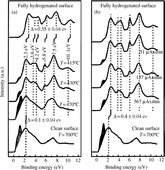
FIGURE 3.6 Photoemission spectra of the H-terminated Si(100) surface as a function of (a) annealing temperature and (b) irradiation dose (annealed clean surface is shown for comparison). Reprinted with permission from Ref. 68. Copyright 2001 American Physical Society.
In contrast to the clean H-terminated silicon and germanium surfaces, H-terminated diamond(100) surfaces have different characteristics. Compared to the rapid oxidation of H-terminated silicon surfaces after exposure to ambient conditions, the H-terminated diamond(100) surfaces are stable in air for many weeks. H-terminated diamond surfaces have a negative electron affinity [69,70]. C–H bonds terminating diamond surfaces create a surface dipole and cause the significant upwards band bending of the valence and conduction band, resulting in the conduction band shifting above the vacuum level. Therefore, the electrons will be spontaneously emitted when the H-terminated diamond surface is irradiated with light. In addition, diamond surfaces are converted into conducting p-type semiconductor surfaces upon hydrogenation because the surface bound hydrogen atoms play the role of a dopant by being directly responsible for the hole accumulation layer, forming shallow electron acceptors [71,72]. The surface states of hydrogen on the H-terminated diamond(100) surface have also been monitored by photoemission spectra. C–H surface states are observed at 8.8, 11.4, and 16.9 eV, which disappear after hydrogen removal but can be recovered after hydrogenation [73].
3.3.6 Reactivity of Partially H-Terminated Semiconductor Surfaces Under Vacuum
For partially H-terminated semiconductor surfaces, the regenerated dangling bonds as the active sites exhibit reactivity with other atoms or molecules. Reactions of organic and inorganic molecules on such partially hydrogenated semiconductor surfaces have been studied. Single dangling bonds, created on fully H-terminated Si (100) surfaces by STM, can adsorb one incoming molecule. At this level, rationally designed surfaces with special properties can be obtained. Many large molecules such as norbornadiene, copper phthalocyanine (CuPc), and C60 have been studied on the partially H-terminated Si(100) surface through this method [74]. However, the binding of a single molecule to one dangling bond does not occur in the same way due to the existence of multifunctional groups in large molecules. For example, CuPc attached the silicon dangling bonds through the center copper atoms or through π-interaction with pyrrole groups [74].
Of particular interest is the local manipulation of hydrogen atoms and the subsequent promotion of surface reactivity at these sites for the growth of organic nanostructures through surface reaction mechanisms [75–77]. The growth of atomic wires of styrene on partially H-terminated Si(100) has been reported through radical generation and a hydrogen abstraction mechanism as shown in Fig. 3.7 [76]. A bias is applied to a specific hydrogen atom to generate a surface silicon dangling bond. The adsorption of a styrene molecule on this single dangling bond creates a radical on the vinyl group. This vinyl group withdraws one hydrogen atom from an adjacent dimer terminated with hydrogen atoms, creating another dangling bond site on this dimer. This alternating creation of dangling bonds on a silicon dimer and a radical on a vinyl group leads to the formation of an atomic wire. The growth is terminated at a defect site on the dimer row.
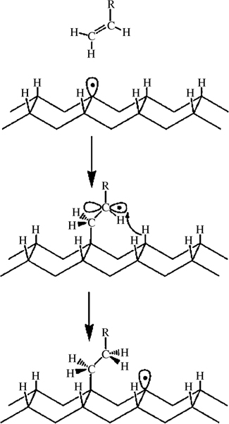
FIGURE 3.7 Proposed chain reaction mechanism for the growth of molecular nanostructures on partially H-terminated Si(100) surface. This involves the reaction of an alkene with a single dangling bond on an otherwise hydrogen-terminated Si(100) surface. Reprinted with permission from Ref. 76. Copyright 2000 Nature Publication Group.
3.4 GEOMETRY AND ELECTRONIC STRUCTURE OF HALOGEN-TERMINATED SEMICONDUCTOR SURFACES
Interactions between halogens and semiconductor surfaces are important to semiconductor etching processes as well as other surface functionalizations. In this section, the preparation and structure of halogen-terminated semiconductor surfaces are presented. The reactivity of halogen-terminated semiconductor surfaces via wet chemistry methods will be discussed in the next part. Similar to hydrogen, halogens require only one electron to form a closed-shell electronic structure on the surfaces. As a result, halogens can readily react with the semiconductor surfaces and terminate dangling bonds. The halogen-terminated semiconductor surfaces can be synthesized by exposing clean semiconductor surfaces to various halogen sources under UHV or by reacting them with H-terminated semiconductor surfaces.
3.4.1 Preparation of Halogen-Terminated Semiconductor Surfaces Under UHV
Exposure of clean semiconductor surfaces to halogen precursors (Cl2, Br2, etc.) leads to the formation of halogen-terminated semiconductor surfaces. One of the examples is the Cl-terminated Si(100)-(2×1) surface. At low coverage, a metastable bridge-bonded configuration can be observed as shown in Fig. 3.8b [78]. Annealing at 673K, the bridge-bonded configuration converts into stable monochloride configuration (Fig. 3.8c) [78]. At one monolayer of Cl coverage, the monochloride structure was observed on Si(100) surfaces [79,80]. At higher Cl2 exposure, dichloride structures are observed [81]. Br-terminated Si(100) surface shows a similar structure as that of Cl-terminated surfaces. SiBr2 and SiBr3 species are also observed [82]. When the temperature is higher than 850K, desorption of Br atoms lead to the formation of (3×1) structures, in which two SiBr monobromide dimers alternate with vacancies as shown in Fig. 3.8d. At higher temperature (>900°C), (3×1) structures are not observed due to the rapid desorption of SiBrx.
In contrast to numerous studies on halogen-terminated Si(100)-(2×1) surfaces, the adsorption of halogen atoms on Ge(100)-(2×1) and diamond(100)-(2×1) surfaces have been studied less intensively. This is partially due to the less active surfaces of Ge(100) and diamond(100) compared to that of Si(100)-(2×1). Currently, experimental data available for the adsorption of iodine on the Ge(100)-(2×1) surface. STM investigation has shown the dominant GeI species with minor GeI2 structure under low coverage [83,84].
For Cl-terminated Si(111)-(7×7) surfaces, STM studies indicate the formation of Cl-terminated adatoms at low coverage [85,86]. Upon further exposure to chlorine, Cl atoms insert into backbonds between the adatom and rest atom layer. Further exposure breaks one of the bonds between the chlorinated adatom and rest atom, producing a SiCl3 group bonded directly above a rest atom layer. Saturated coverage leads to the formation of SiCl, SiCl2, and SiCl3 species [87]. Annealing a saturated surface at 675K causes surface reconstruction in which the rest atom layer is exposed, with all atoms terminated by Cl, and adatoms made up of higher SiClx species agglomerated together into small islands [87].
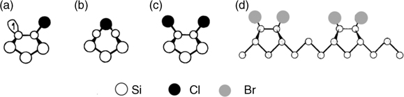
FIGURE 3.8 Structural model of halogens on Si(100), showing hemichloride (a), bridge-bonded structure (b), monochloride (c), and (3×1) structures (d). Reprinted with permission from Ref. 12. Copyright 1996 American Chemical Society.
3.4.2 Preparation of Halogen-Terminated Semiconductor Surfaces from H-Terminated Semiconductor Surfaces
The halogen-terminated semiconductor surface can be prepared by starting from H-terminated semiconductor surfaces. Two known methods involve treating H-terminated silicon surfaces with PCl5 [88] at 80–100°C and N-bromosuccinimide [85] at 60°C using benzoyl peroxide as a radical initiator. Cl2 or CCl3Br can initiate the conversion from H-terminated silicon surfaces into halogen-terminated silicon surfaces [88–91]. A chlorinated germanium surface can be prepared by a reaction with gaseous HCl or 10% aqueous HCl on Ge(111) wafers pretreated with H2O2 and oxalic acid [92,93].
3.5 REACTIVITY OF HYDROGEN- OR HALOGEN-TERMINATED SEMICONDUCTOR SURFACES IN SOLUTION
Surface modification of semiconductor surfaces under UHV conditions is costly under restricted reaction conditions. Therefore, various methods have been developed for semiconductor surface functionalization in solution starting from hydrogen- or halogen-terminated surfaces, such as radical-initiated hydrosilylation, thermal-driven hydrosilylation, photomediated hydrosilylation, metal complex-catalyzed hydrosilylation, electrochemical grafting, Grignard-related hydrosilylation, and mechanical carving with simultaneous hydrosilylation. In addition, chlorinated germanium surfaces can be functionalized by using ethyl Grignard reagents. These methods have all been well reviewed [2,8].
3.5.1 Reactivity of Si and Ge Surfaces in Solution
The reaction mechanisms for hydrogen- or halogen-terminated Si surfaces are summarized in Fig. 3.9. For radical-initiated hydrosilylation, a chemical with an unsaturated bond reacts with surface Si–H or Ge–H bonds, forming an alkenyl or alkyl monolayer through the formation of Si–C or Ge–C covalent bonds [94,95]. Generally, this type of reaction is processed by a radical initiator. Diacyl peroxide is often used to decompose and form an alkyl radical, which can abstract a hydrogen atom from the surface silicon and forms a surface silicon radical. This silicon radical can rapidly react with an unsaturated bond of an organic molecule and therefore form a radical on the carbon of the immobilized organic chain. The radical on carbon chain then takes a hydrogen atom from its adjacent Si–H bond and forms surface silicon radical. The reaction mechanism of such a reaction is illustrated in Fig. 3.9a. In the absence of radical initiator, hydrosilylation can be induced by a thermal or photo initiators. High temperature, generally 150–200°C, promotes the cleavage of surface Si–H bond to generate silicon radicals on silicon surfaces [94–101]. Such a radical on a silicon atom shows the same activity as that of hydrosilylation with the radical initiator. Photolysis is an alternative method to break Si–H bonds and generate surface silicon radicals for further reaction with unsaturated bonds of organic molecules [91,102–106]. Hydrosilylation with the radical initiator happens homogenously in the solution without area selectivity. Thermally driven hydrosilylation may damage the semiconductor surfaces due to high temperature. In contrast, photo-driven hydrosilylation is promising in applications due to its selective exposure area and low temperature. By using masks with different sizes, shapes, and/or multiple beams with certain pattern and spot size, semiconductor surfaces can be selectively functionalized [91,102,103,105–107].
FIGURE 3.9 Reaction mechanisms for organic functionalization of hydrogenated and halogenated semiconductor surfaces in solution: (a) radical-initiated hydrosilylation, thermal-driven hydrosilylation, and photomediated hydrosilylation; (b) metal complex-catalyzed hydrosilylation; (c) electrochemical grafting; (d) Grignard-related hydrosilylation and halogenosilylation; and (e) mechanical carving and simultaneous hydrosilylation in solution. Reprinted with permission from Ref. 8. Copyright 2009 American Chemical Society.
The second method for surface hydrosilyation at liquid–solid interfaces is assisted by the presence of catalysts. Similar to the catalytic reactions between alkenes with silanes in classical organic chemistry, Pt(0) complexes can catalyze hydrosilylation at the liquid-solid interface between unsaturated organic molecules and a H-terminated silicon surface in solution as shown in Fig. 3.9b [108]. Notably, the Pt(0) complex can catalyze oxidation between the silicon surfaces and a trace amount of water or oxygen in solution. Lewis acid catalysts can also be used as an alternative route for surface hydrosilyation to avoid the possible surface oxidation [109–111]. Lewis acids have been successfully used to functionalize H-terminated Si(111) surfaces with various organic compounds at a relatively high temperature, such as 100°C.
Electrochemistry-based functionalization can avoid the problem of oxidation during the hydrosilyation process thanks to the electron-rich cathode, which draws nucleophilic attacks of water. Aryl radicals can be generated by applying a negative potential of 1 V in an electrolyte containing HF and bromobenzene diazonium salt. Then, aryl radicals can initiate surface modification by replacing hydrogen atom and forming Si–C covalent bonds on H-terminated silicon surfaces [112,113].
The addition of organolithium and Grignard reagents to the silicon surface has been carried out on H-terminated porous silicon surfaces [114]. The reaction proceeds through a transmetalation reaction (Fig. 3.9d1) in which the formation of Si–C bonds results from the attack of the weak Si–Si bonds by a carbanion nucleophile. This approach was also applied to modify the flat silicon surface through a two-step halogenation/alkylation route [88]. Immersion of Cl-terminated silicon substrate into a solution composed of alkyllithium or Grignard at 80° C for various periods of time results in LiCl or MgXCl and an alkyl group bound to silicon substrate through Si–C covalent bond. It is also possible to directly form alkylated silicon surfaces on H-terminated substrate with butyl-, hexyl-, phenyl-, and 5-(N-pyrrolyl)pentyllithium reagents in THF at room temperature [115]. The reaction is similar to that of H-terminated porous silicon, by which cleavage of the relatively weak Si–Si bond leads to attachment of the organic molecule. Direct alkylation on H-terminated Si(111) was also observed with decylmagnesium bromide in diethyl ether for 16 h [105]. Since there are no Si–Si surface bonds on H-terminated Si(111), the reaction was suggested to proceed through cleavage of Si–H bonds.
The last pathway involves mechanical removal of the native oxide and instant chemical functionalization in solution. The removal of natural oxide creates dangling bonds that may exhibit reactivity similar to that of a Si=Si dimer formed under UHV conditions [116,117]. The possible surface reactions are listed in Fig. 3.9e.
In contrast to rich surface chemistry on hydrogen- or halogen-terminated Si surfaces in solution, Ge surfaces are seldom studied. There are two reported approaches for functionalization of Ge surfaces. The first method is that of alkyl Grignard reagent reacting with the halogen-terminated Ge(111) surface, forming an alkylated Ge surface [118]. The other approach is hydrogermylation of the H-terminated Ge(100) surface by inserting unsaturated C–C bonds into the Ge–H bond [119].
3.5.2 Reactivity of Diamond Surfaces in Solution
The high stability of H-terminated diamond(100) surfaces makes it extremely difficult to functionalize. The first surface reaction on H-terminated diamond (100) was achieved through radical reactions of aryl diazonium salt, similar to the radical reactions on silicon surfaces [120,121]. The pioneering work of alkenes grafting to the diamond surface was carried out via C=C group activated by a 254 nm light [122]. The original work used robust diamond surfaces for fabricating a DNA biosensor. The trifluoroacetamide-protected 10-aminodec-1-ene (TFAAD) was photografted on the H-terminated diamond(100) surface as shown in Fig. 3.10a. Compared to devices based on other surfaces, diamond and glassy carbon exhibit the best stability. The stability is not only attributed to the diamond but is also a consequence of the intrinsic stability of the interface C–C bond.
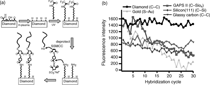
FIGURE 3.10 (a) Schematic showing the steps in covalent bonding of DNA to diamond. Reprinted with permission from Ref. 10. Copyright 2009 American Chemical Society. (b) Stability of DNA-modified surfaces in repeated cycles of hybridization and denaturation using 8.3 M urea. Reprinted with permission from Ref. 122. Copyright 2003 Nature Publishing Group.
The photografting reaction of alkenes on H-terminated diamond is quite vague, because diamond (5.48 eV band gap, 226 nm) and most organic alkenes are almost completely transparent to the most commonly used light source (254 nm). For the photografting reactions of H-terminated silicon surface, light with energy larger than the band gap of silicon creates electron-hole pairs in silicon [105,106]. It is critical to understand the behavior of a transparent substrate and a transparent alkene under light illumination. Experiments have discovered that surface activity of photografting is related to the functional groups of the alkene molecules [123,124]. TFAAD grafting was much faster than that of tert-butyl oxycarbamate (tBoc) grafting and photografting of 1-dodecene was almost undetectable under the same conditions on diamond surfaces. Energy-level differences of diamond and bifunctional molecules are used to explain the different behavior of the surface photografting. Bifunctional alkenes have similar donor levels, but their acceptor levels are quite different as shown in Fig. 3.11a. Trifluoroacetamide group of TFAAD is a good electron acceptor and its affinity level is below the conduction band of diamond. Such an electronic structure favors electron transfer from the diamond surface to the organic molecule, leading to the highest reactivity. tBoc and 1-dodecene have higher affinity levels, and consequently, are less reactive. Fig. 3.11b shows the photoemission spectra of TFAAD and tBoc on the diamond(100) surface, which directly monitors electrons ejected from the valence band of diamond into acceptor levels of adjacent molecules.
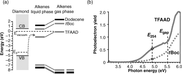
FIGURE 3.11 Photoemission initiation of grafting of alkenes to diamond: (a) energy-level diagrams for donor and acceptor levels; (b) direct measurements of photoelectron emission from diamond into TFAAD and tBoc. Reprinted with permission from Ref. 124. Copyright 2009 American Chemical Society.
For TFAAD, significant photoemission yields are observed at 3.9 eV, below the band gap of diamond. Actually, this value is close to the gap between the diamond valence band and the TFAAD affinity level. The difference in photoelectron yield at 254 nm between TFAAD and tBoc corresponds to the differences in reactivity.
3.6 SUMMARY
Significant efforts have been taken to understand the organic reactions on semiconductor surfaces, including experimental techniques and theoretical predictions, especially for Si(100), Ge(100), diamond(100), and Si(111) surfaces. The semiconductor surface geometry and electronic structure are extremely important in understanding surface reactivity with organic molecules and hence obtain controllable functionalization on semiconductor surfaces. The clean surface of Si(100), Ge(100), and diamond(100) undergo (2×1) reconstruction and form surface dimers to achieve a minimum energy state. Asymmetrical dimers for Si(100) and Ge(100) and symmetrical dimers for diamond(100) have different electronic structures and result in higher reactivity with organic molecules on Si(100) and Ge(100) surfaces. The pair of adatoms and rest atoms of Si(111)-(7×7) surface are similar to surface dimers of Si(100)-(2×1) surface, resulting in high surface reactivity toward surface organic reactions. H-terminated semiconductor surfaces always show weak reactivity due to their high stability. Partially H-terminated semiconductor surfaces with dangling bonds exhibit controllable surface modification on selective areas. Various methods including radical initiation, catalysts, and electrochemistry have been introduced to activate surface functionalization on hydrogen- or halogen-terminated semiconductor surfaces with organic molecules with unsaturated groups. Future investigations will focus on the interface of semiconductor surfaces with controllable properties at selected areas at the molecular level for wide applications of organic–inorganic hybrid devices.
ACKNOWLEDGMENTS
This work was supported by NKBRSF (No. 2007CB815202), NSFC (No. 20833008), and 863 (Nos. 2006AA01A119, 2009AA01A130).
REFERENCES
1. Mayne, A. J.; Riedel, D.; Comtet, G.; Dujardin, G. Prog. Surf. Sci. 2006, 81, 1.
2. Buriak, J. M. Chem. Rev. 2002, 102, 1271.
3. Wolkow, R. A. Annu. Rev. Phys. Chem. 1999, 50, 413.
4. Filler, M. A.; Bent, S. F. Prog. Surf. Sci. 2003, 73, 1.
5. Hamers, R.J.; Coulter, S. K.;Ellison, M. D.; Hovis, J. S.; Padowitz, D. F.; Schwartz, M. P.; Greenlief, C. M.; Russell, J. N. Acc. Chem. Res. 2000, 33, 617.
6. Leftwich, T. R.; Teplyakov, A. V. Surf. Sci. Rep. 2008, 63, 1.
7. Tao, F.; Xu, G. Q. Acc. Chem. Res. 2004, 37, 882.
8. Tao, F.; Bernasek, S. L.; Xu, G. Q. Chem. Rev. 2009, 109, 3991.
9. Ristein, J. Surf. Sci. 2006, 600, 3677.
10. Wang, X. Y.; Landis, E. C.; Franking, R.; Hamers, R. J. Acc. Chem. Res. 2010, 43, 1205, doi10.1021/ar100011f.
11. Hamers, R. J.; Wang, Y. J. Chem. Rev. 1996, 96, 1261.
12. Simpson, W. C.; Yarmoff, J. A. Annu. Rev. Phys. Chem. 1996, 47, 527.
13. Rodriguez-Reyes, J. C. F.; Teplyakov, A. V. Chemistry 2007, 13, 9164.
14. Binnig, G.; Rohrer, H. Helve. Phys. Acta. 1982, 55, 726.
15. Binnig, G.; Rohrer, H.; Gerber, C.; Weibel, E. Phys. Rev. Lett. 1983, 50, 120.
16. Schlier, R. E.; Farnsworth, H. E. J. Chem. Phys. 1959, 30, 917.
17. Phillips, J. C. Surf. Sci. 1973, 40, 459.
18. Poppendieck, T. D.; Gnoc, T. C.; Webb, M. B. Surf. Sci. 1974, 43, 647.
19. Appelbaum, J. A.; Baraff, G. A.; Hamann, D. R. Phys. Rev. B 1976, 14, 588.
20. Appelbaum, J. A.; Baraff, G. A.; Hamann, D. R. Phys. Rev. Lett. 1975, 35, 729.
21. Appelbaum, J. A.; Baraff, G. A.; Hamann, D. R.; Hagstrum, H. D.; Sakurai, T. Surf. Sci. 1978, 70, 654.
22. Hamers, R. J.; Tromp, R. M.; Demuth, J. E. Phys. Rev. B 1986, 34, 5343.
23. Tromp, R. M.; Hamers, R. J.; Demuth, J. E. Phys. Rev. Lett. 1985, 55, 1303.
24. Hamers, R. J.; Tromp, R. M.; Demuth, J. E. Surf. Sci. 1987, 181, 346–355.
25. Wolkow, R. A. Phys. Rev. Lett. 1992, 68, 2636.
26. Weakliem, P. C.; Carter, E. A. J. Chem. Phys. 1992, 96, 3240.
27. Tabata, T.; Aruga, T.; Murata, Y. Surf. Sci. 1986, 179, L63.
28. Wu, C. J.; Carter, E. A. Chem. Phys. Lett. 1991, 185, 172.
29. Develyn, M. P.; Yang, Y. M. L.; Sutcu, L. F. J. Chem. Phys. 1992, 96, 852.
30. Hofer, U.; Li, L. P.; Heinz, T. F. Phys. Rev. B 1992, 45, 9485.
31. Nachtigall, P.; Jordan, K. D.; Sosa, C. J. Phys. Chem. 1993, 97, 11666.
32. Flowers, M. C.; Jonathan, N. B. H.; Liu, Y.; Morris, A. J. Chem. Phys. 1993, 99, 7038.
33. Mui, C.; Bent, S. F.; Musgrave, C. B. J. Phys. Chem. A 2000, 104, 2457.
34. Carey, F. A.; Sundberg, R. J. Advanced Organic Chemistry. Plenum Publishing Corporation, 2001.
35. Konecny, R.; Doren, D. J. J. Chem. Phys. 1997, 106, 2426.
36. Kubby, J. A.; Griffith, J. E.; Becker, R. S.; Vickers, J. S. Phys. Rev. B 1987, 36, 6079.
37. Hovis, J. S.; Coulter, S. K.; Hamers, R. J.; D'Evelyn, M. P.; Russell, J. N.; Butler, J. E. J. Am. Chem. Soc. 2000, 122, 732.
38. Woodward, R. B.; Hoffmann, R. The Conservation of Orbital Symmetry. Academic Press, New York, 1970.
39. Cricenti, A.; Purdie, D.; Reihl, B. Surf. Sci. 1995, 331, 1033.
40. Wormeester, H.; Wentink, D. J.; Deboeij, P. L.; Wijers, C. M. J.; Vansilfhout, A. Phys. Rev. B 1993, 47, 12663.
41. Mercer, T. W.; Pehrsson, P. E. Surf. Sci. 1998, 399, L327.
42. Choi, C. H.; Gordon, M. S. J. Am. Chem. Soc. 1999, 121, 11311.
43. Liu, Q.; Hoffmann, R. J. Am. Chem. Soc. 1995, 117, 4082.
44. Lal, P.; Teplyakov, A. V.; Noah, Y.; Kong, M. J.; Wang, G. T.; Bent, S. F. J. Chem. Phys. 1999, 110, 10545.
45. Mui, C.; Han, J. H.; Wang, G. T.; Musgrave, C. B.; Bent, S. F. J. Am. Chem. Soc. 2002, 124, 4027.
46. Li, J.; Qu, Y. Q.; Han, K. L.; He, G. Z. Surf. Sci. 2005, 586, 45.
47. Qu, Y. Q.; Han, K. L. J. Phys. Chem. B 2004, 108, 8305.
48. Qu, Y. Q.; Li, J.; Han, K. L. J. Phys. Chem. B 2004, 108, 15103.
49. Qu, Y. Q.; Wang, Y.; Li, J.; Han, K. L. Surf. Sci. 2004, 569, 12.
50. Cao, X. P.; Hamers, R. J. J. Phys. Chem. B 2002, 106, 1840.
51. Takayanagi, K.; Tanishiro, Y.; Takahashi, M.; Takahashi, S. J. Vac. Sci. Technol. A 1985, 3, 1502.
52. Landstrass, M. I., Ravi, K. V. Appl. Phys. Lett. 1989, 55, 975.
53. Boland, J. J. Adv. Phys. 1993, 42, 129.
54. Boland, J. J. Phys. Rev. Lett. 1990, 65, 3325.
55. Boland, J. J. Phys. Rev. Lett. 1991, 67, 1539.
56. Sakurai, T.; Hagstrum, H. D. Phys. Rev. B 1976, 14, 1593.
57. Boland, J. J. J. Phys. Chem. 1991, 95, 1521.
58. Burrows, V. A.; Chabal, Y. J.; Higashi, G. S.; Raghavachari, K.; Christman, S. B. Appl. Phys. Lett. 1988, 53, 998.
59. Higashi, G. S.; Chabal, Y. J.; Trucks, G. W.; Raghavachari, K. Appl. Phys. Lett. 1990, 56, 656.
60. Chabal, Y. J. Physica B 1991, 170, 447.
61. Dumas, P.; Chabal, Y.; Jakob, P. Surf. Sci. 1992, 269/270, 867.
62. Higashi, G. S.; Becker, R. S.; Chabal, Y. J.; Becker, A. J. Appl. Phys. Lett. 1991, 58, 1656.
63. Thoms, B. D.; Owens, M. S.; Butler, J. E.; Spiro, C. Appl. Phys. Lett. 1994, 65, 2957.
64. Boland, J. J. Phys. Rev. B 1991, 44, 1383.
65. Naitoh, M.; Morioka, H.; Shoji, F. Surf. Sci. 1993, 297, 135.
66. Sinniah, K.; Sherman, M. G.; Lewis, L. B.; Weinberg, W. H.; Yates, J. T., Jr.,; Janda, K. C. Phys. Rev. Lett. 1989, 62, 567.
67. Boland, J. J. J. Vac. Sci. Technol. A 1992, 10, 2458.
68. Bobrov, K.; Comtet, G.; Dujardin, G.; Hellner, L. Phys. Rev. Lett. 2001, 86, 2633.
69. Diederich, L.; Kuttel, O.; Aebi, P.; Schlapbach, L. Surf. Sci. 1998, 418, 219.
70. Maier, F.; Ristein, J.; Ley, L. Phys. Rev. B 2001, 64, 165411.
71. Landstrass, M. I.; Ravi, K. V. Appl. Phys. Lett. 1989, 55, 1391.
72. Looi, H. J.; Pang, L. Y. S.; Molloy, A. B.; Jones, F.; Foord, J. S.; Jackman, R. B. Diam. Relat. Mater. 1998, 7, 550.
73. Bobrov, K.; Comtet, G.; Dujardin, G.; Hellner, L. Surf. Sci. 2001, 482, 437.
74. Hersam, M. C.; Guisinger, N. P.; Lyding, J. W. Silicon-Based Molecular Nanotechnology, Nanotechnology II, 2000, p. 70.
75. Kato, K.; Kajiyama, H.; Heike, S.; Hashizume, T.; Uda, T. Phys. Rev. Lett. 2001, 86, 2842.
76. Lopinski, G. P.; Wayner, D. D. M.; Wolkow, R. A. Nature 2000, 406, 48.
77. Piva, P. G.; DiLabio, G. A.; Pitters, J. L.; Zikovsky, J.; Rezeq, M.; Dogel, S.; Hofer, W. A.; Wolkow, R. A. Nature 2005, 435, 658.
78. Cheng, C. C.; Gao, Q.; Choyke, W. J.; Yates, J. T., Jr., Phys. Rev. B 1992, 46, 810.
79. Szabo, Z.; Farral, P. D.; Engel, T. Surf. Sci. 1994, 312, 284.
80. Gao, Q.; Cheng, C. C.; Chen, P. J.; Choyke, W. J.; Yates, J. T., Jr., J. Chem. Phys. 1993, 98, 8308.
81. Bronikowski, M. J.; Hamers, R. J. J. Vac. Sci. Technol. A 1995, 13, 777.
82. Rioux, D.; Chander, M.; Li, Y. Z.; Weaver, J. H. Phys. Rev. B 1994, 49, 11071.
83. Gothelid, M.; Le Lay, G.; Wigren, C.; Bjorkqvist, M.; Karlsson, U. O. Surf. Rev. Lett. 1998, 5, 119.
84. Gothelid, M.; Le Lay, G.; Karlsson, U. O. Surf. Sci. 2004, 556, 203.
85. Boland, J. J.; Villarrubia, J. S. Science 1990, 248, 838.
86. Boland, J. J.; Villarrubia, J. S. Phys. Rev. B: Condens. Matter 1990, 41, 9865.
87. Schnell, R. D.; Rieger, D.; Bogen, A.; Wandelt, K.; Steinmann W. Solid State Commun. 1985, 53, 205.
88. Bansal, A.; Li, X. L.; Lauermann, I.; Lewis, N. S.; Yi, S. I.; Weinberg, W. H. J. Am. Chem. Soc. 1996, 118, 7225.
89. He, J.; Patitsas, S. N.; Preston, K. F.; Wolkow, R. A.; Wayner, D. D. M. Chem. Phys. Lett. 1998, 286, 508.
90. Zhu, X. Y.; Boiadjiev, V.; Mulder, J. A.; Hsung, R. P.; Major, R. C. Langmuir 2000, 16, 6766.
91. Terry, J.; Linford, M. R.; Wigren, C.; Cao, R. Y.; Pianetta, P.; Chidsey, C. E. D. Appl. Phys. Lett. 1997, 71, 1056.
92. Lu, Z. H. Appl. Phys. Lett. 1996, 68, 520.
93. Choi, K.; Buriak, J. M. Langmuir 2000, 16, 7737.
94. Linford, M. R.; Fenter, P.; Eisenberger, P. M.; Chidsey, C. E. D. J. Am. Chem. Soc. 1995, 117, 3145.
95. Chatgilialoglu, C. Acc. Chem. Res. 1992, 25, 188.
96. Sung, M. M.; Kluth, G. J.; Yauw, O. W.; Maboudian, R. Langmuir 1997, 13, 6164.
97. Sieval, A. B.; Vleeming, V.; Zuilhof, H.; Sudholter, E. J. R. Langmuir 1999, 15, 8288.
98. Sieval, A. B.; Linke, R.; Heij, G.; Meijer, G.; Zuilhof, H.; Sudholter, E. J. R. Langmuir 2001, 17, 7554.
99. Bateman, J. E.; Eagling, R. D.; Worrall, D. R.; Horrocks, B. R.; Houlton, A. Angew. Chem., Int. Ed. 1998, 37, 2683.
100. Boukherroub, R.; Morin, S.; Wayner, D. D. M.; Bensebaa, F.; Sproule, G. I.; Baribeau, J. M.; Lockwood, D. J. Chem. Mater. 2001. 13, 2002.
101. Bateman, J. E.; Eagling, R. D.; Horrocks, B. R.; Houlton, A. J. Phys. Chem. B 2000, 104, 5557.
102. Terry, J.; Mo, R.; Wigren, C.; Cao, R. Y.; Mount, G.; Pianetta, P.; Linford, M. R.; Chidsey, C. E. D. Nucl. Instrum. Methods Phys. Res., Sect. B 1997, 133, 94.
103. Terry, J.; Linford, M. R.; Wigren, C.; Cao, R. Y.; Pianetta, P.; Chidsey, C. E. D. J. Appl. Phys. 1999, 85, 213.
104. Cicero, R. L.; Linford, M. R.; Chidsey, C. E. D. Langmuir 2000, 16, 5688.
105. Stewart, M. P.; Buriak, J. M. Angew. Chem., Int. Ed. 1998, 37, 3257.
106. Stewart, M. P.; Buriak, J. M. J. Am. Chem. Soc. 2001, 123, 7821.
107. Imanishi, A.; Yamane, S.; Nakato, Y. Langmuir 2008, 24, 10755.
108. Lewis, L. N. J. Am. Chem. Soc. 1990, 112, 5998.
109. Boukherroub, R.; Morin, S.; Bensebaa, F.; Wayner, D. D. M. Langmuir 1999, 15, 3831.
110. Buriak, J. M.; Allen, M. J. J. Am. Chem. Soc. 1998, 120, 1339.
111. Buriak, J. M.; Stewart, M. P.; Geders, T. W.; Allen, M. J.; Choi, H. C.; Smith, J.; Raftery, D.; Canham, L. T. J. Am. Chem. Soc. 1999, 121, 11491.
112. deVilleneuve, C. H.; Pinson, J.; Bernard, M. C.; Allongue, P. J. Phys. Chem. B 1997, 101, 2415.
113. Hurley, P. T.; Ribbe, A. E.; Buriak, J. M. J. Am. Chem. Soc. 2003, 125, 11334.
114. Viellard, C.; Warntjes, M.; Ozanam, F.; Chazalviel, J.-N. Proc. Electrochem. Soc. 1996, 95, 250.
115. Kim, N. Y.; Laibinis, P. E. J. Am. Chem. Soc. 1999, 121, 7162.
116. Niederhauser, T. L.; Jiang, G. L.; Lua, Y. Y.; Dorff, M. J.; Woolley, A. T.; Asplund, M. C.; Berges, D. A.; Linford, M. R. Langmuir 2001, 17, 5889.
117. Niederhauser, T. L.; Lua, Y. Y.; Sun, Y.; Jiang, G. L.; Strossman, G. S.; Pianetta, P.; Linford, M. R. Chem. Mater. 2002, 14, 27.
118. He, J. L.; Lu, Z. H.; Mitchell, S. A.; Wayner, D. D. M. J. Am. Chem. Soc. 1998, 120, 2660.
119. Sharp, I. D.; Schoell, S. J.; Hoeb, M.; Brandt, M. S.; Stutzmann, M. Appl. Phys. Lett. 2008, 92, 223306.
120. Allongue, P.; Delamar, M.; Desbat, B.; Fagebaume, O.; Hitmi, R.; Pinson, J.; Save′ant, J. M. J. Am. Chem. Soc. 1997, 119, 201.
121. Kuo, T. C.; McCreery, R. L.; Swain, G. M. Electrochem. Solid State Lett. 1999, 2, 288–290.
122. Yang, W. S.; Auciello, O.; Butler, J. E.; Cai, W.; Carlisle, J. A.; Gerbi, J. E.; Gruen, D. M.; Knickerbocker, T.; Lasseter, T. L.; Russell, J. N., Jr.,; Smith, L. M.; Hamers, R. J. Nat. Mater. 2002, 1, 253.
123. Wang, X.; Colavita, P. E.; Metz, K.M.; Butler, J. E.; Hamers, R.J. Langmuir 2007, 23, 11623.
124. Wang, X.; Colavita, P. E.; Streifer, J. A.; Butler, J. E.; Hamers, R. J. J. Phys. Chem. C 2009, 114, 4067–4074.
Functionalization of Semiconductor Surfaces, First Edition
Edited by Franklin (Feng) Tao and Steven L. Bernasek.
© 2012 John Wiley & Sons, Inc. Published 2012 by John Wiley & Sons, Inc.