
CHAPTER 11
Formation of Organic Monolayers Through Wet Chemistry
DAMIEN AUREAU AND YVES J. CHABAL
11.1 INTRODUCTION, MOTIVATION, AND SCOPE OF CHAPTER
11.1.1 Background
Wet chemical cleaning has always been an intrinsic part of semiconductor processing [1,2], but only relatively recently has wet chemistry been used to modify semiconductor surfaces for sensitive applications. Wet chemical functionalization is attractive because it can be performed in reasonably manageable environments and is scalable. Wet chemical cleaning, for instance, which constitutes ~30% of silicon processing in microelectronics, can be performed for entire cassettes of wafers in regular clean rooms. Clean chemicals have also been developed for such large-scale use. In general, wet chemical processing is simpler and more versatile than ultrahigh vacuum (UHV) methods, and can often lead to more perfect surfaces than what can be achieved in UHV [3–8].
Silicon has been central to the microelectronics industry for one main reason. Its oxide is stable and the interface between silicon and its oxide is electrically much better than for any other semiconductor surface, in particular germanium [9]. It is therefore not surprising that the early work on silicon surface functionalization has focused on attaching organic molecules to silicon oxide, using silanization for instance [10]. Typically, silanization is based on hydrolyzing molecules such as triethoxysilanes or trichlorosilanes with hydroxyl-terminated silicon oxide in the presence of water molecules. It has become apparent, however, that this process is strongly dependent on the density of initial surface hydroxyl groups, the amount of water molecules present in their vicinity, and temperature, leading to uncontrolled attachment [11]. These molecules also have a tendency to polymerize, making the formation of a single self-assembled monolayer (SAM) virtually impossible. An alternative process involves phosphonates that are not water sensitive and can therefore be attached on native oxide surfaces in ambient environments [12,13]. However, this process is not yet well understood and does not readily lead to well-defined layers [13,14].
The performance of the sensors in terms of reliability, efficiency, and sensitivity generally depends on the control of the immobilization chemistry of the probes [15]. Yet, most electronic applications such as biological and chemical sensors to date are using silane [16] or phosphonate [17] chemistry because of the electrical quality of the initial Si/SiO2 interface, thereby suffering from poor SAM stability.
The work described in this chapter is based on the premise that silicon oxide is not a good starting point for controlled functionalization, primarily because of the poor control of and film quality resulting from silanization. Indeed, while the Si/SiO2 interface is electrically excellent, the SiO2/organic layer interface is unstable in aqueous environments needed for biological or other applications. The alternative to oxide would be a surface that is stable enough to prevent reoxidation under ambient conditions, yet that can react with organic molecules to form strong covalent bonds. In other words, a metastable atom or molecule must be attached to a clean surface, which is amenable to controlled further reaction [18]. For silicon, hydrogen and halogens have been considered. They can be attached via reasonably straightforward wet chemical procedures and can be further reacted in controllable fashion. Hydrogen-terminated silicon surfaces, for instance, can be produced very simply by HF etching, as described below in some detail.
Another substrate of interest is germanium because it exhibits noted advantages over silicon for microelectronics. Its hole carrier mobility is four times that in silicon, which is important for high-speed circuits and is of interest in CMOS technology where the p-channel component of Si has traditionally had less than ideal performance. Further, the 0.67 eV bandgap of Ge allows the absorption of infrared radiation, which makes Ge, or a SiGe alloy, a suitable rear absorber in a multijunction solar cell [19]. Methods yielding low defect density Ge surfaces have therefore been investigated. However, the high surface state density and the instability and water solubility of Ge oxide have proven to be significant drawbacks to the development of Ge-based technology [20]. Germanium surfaces can be hydrogen terminated in HF but they are much less stable than H-terminated silicon surfaces [21,22], leading to chemically imperfect surfaces upon further processing. Halogenation of germanium surfaces appears to be more stable than H-terminated Ge [23,24]. Sulfide passivation eliminates Ge oxides, but can lead to the formation of a GeS glass [25]. For completeness, however, comparison between wet chemical modification of germanium and silicon will be given in this chapter [9,22,26].
For semiconductors other than silicon and germanium, the situation is more complicated. Silicon carbide features a very stable native or thermally grown silicon oxide. However, removal of the oxide does not lead to hydrogenated or halogenated surfaces. For instance, HF etching leads to the formation of hydrophilic, hydroxyl-terminated surfaces [27] that cannot be readily reacted with organic molecules. In contrast to silicon and silicon carbide, III–V semiconductors have poor native oxides and cannot be easily hydrogen terminated in HF [28]. Instead, they have been passivated by group VI atoms (other than oxygen) or halogens. In particular, sulfur appears to stabilize GaAs and InP surfaces well [29], but the details of such passivation are not well understood. Therefore, organic functionalization of sulfur-passivated GaAs is not as well defined and controlled as needed for most devices.
Surface cleaning and termination constitute the first steps of surface functionalization. For silicon, the most common approach combines aggressive cleaning/oxidizing with peroxides and acids, followed by hydrogen termination obtained by HF etching. To better appreciate the issues associated with stabilizing semiconductor surfaces with hydrogen, it is therefore useful to consider the formation process and the stability of H-terminated silicon surfaces.
11.1.2 Formation of H-Terminated Silicon Surfaces
The unique properties of HF-etched Si surfaces have been recognized over a half-century but the mechanism leading to these hydrophobic surfaces has only been understood a little over two decades. It is now clear that hydrogen and not fluorine terminates the surface [30], and is responsible for hydrophobicity, chemical resistance, and low density of electronic states (i.e., high recombination velocity) [31]. The initial confusion and controversy about H versus F termination was understandable because a trace amount of fluorine is typically found on HF-etched surfaces and the Si–F bond is much stronger (~5 eV) than the Si–H bond (~3.5 eV). The key mechanism was first proposed by Ubara et al. [30,32] on microcrystalline Si [33], and later confirmed by ab initio calculations [4]. In this mechanism summarized in Fig. 11.1, removal of the last oxygen atom in the SiO2 overlayer does indeed lead to the formation of Si–F. However, although this bond is very strong, it is also very polar. The strong polarity polarizes the Si–Si back-bond of Si–Si–F, rendering it vulnerable to further attack by HF. The calculations of Trucks et al. [4] showed that the barrier for attaching H to the back Si of Si–Si–F and releasing the surface Si in the form of SiF4 was only ~1 eV, without including the facilitating effects of solvation. The resulting H-terminated surface is nonpolar and therefore quite resistant to further chemical attack by HF (i.e., there is no further etching in HF solution once the surface is H-terminated) or by other chemical species as summarized later in this introductory section.
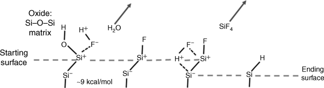
FIGURE 11.1 Mechanism leading to the formation of H-terminated silicon surface by HF etching. The last step of oxygen removal from SiO2 involves HF attack of the Si–O bond, with removal of OH as H2O and termination of the surface Si atom with fluorine. Further attack of the polarized Siδ−–Siδ+ leads to H termination [30].
An important aspect of HF etching is the possibility to induce further etching (i.e., after the surface is H-terminated) when heavily buffered HF solutions are used (pH ~8) [3]. In such solutions (e.g., NH4F), Si–Si bonds can be attacked slowly and selectively. As shown by several studies [5,7,8,34,35], the new etching mechanism involves the OH− ions or related complexes with preferential removal of adstructures and attack of steps, leading to highly structured surfaces. In particular, atomically flat and perfectly monohydride-terminated Si(111) surfaces are obtained on well-oriented ![]() 111
111![]() Si surfaces, atomically straight and H-terminated steps are formed on vicinal
Si surfaces, atomically straight and H-terminated steps are formed on vicinal ![]() 111
111![]() Si surfaces [8,35], and well-defined flat surfaces (with double layer structures) [36] result from etching in NH4F. The main mechanism proposed for the formation of atomically flat, monohydride-terminated surfaces is based on site-specific reactions [7], leading to a step flow etching. The exact chemical reactions have not been fully described, but it is clear that the surface structure plays a key role. The importance of surface structure has been emphasized here because it is central to surface chemistry and therefore surface chemical functionalization, as will be dramatically illustrated in section 11.6 of this chapter. It is also important when considering the stability of H-terminated surfaces as summarized below.
Si surfaces [8,35], and well-defined flat surfaces (with double layer structures) [36] result from etching in NH4F. The main mechanism proposed for the formation of atomically flat, monohydride-terminated surfaces is based on site-specific reactions [7], leading to a step flow etching. The exact chemical reactions have not been fully described, but it is clear that the surface structure plays a key role. The importance of surface structure has been emphasized here because it is central to surface chemistry and therefore surface chemical functionalization, as will be dramatically illustrated in section 11.6 of this chapter. It is also important when considering the stability of H-terminated surfaces as summarized below.
11.1.3 Stability of H-Terminated Silicon Surfaces
Stability and selective reactivity of H-terminated surfaces are essential components of the functionalization process. While stability of chemically passivated Si surfaces will be addressed in more detail in Chapter 12, we highlight here the essential findings for H-terminated Si surfaces.
It is well known that H-terminated Si surfaces, while mostly stable in clean solutions or gases, are degraded as soon as they become exposed to air. For instance, the surface recombination velocity increases by an order of magnitude when a Si sample is removed from the HF solution [31], and some initial oxidation is often observed after several hours in air. Yet, series of experiments performed in very well-controlled environments have revealed that H-terminated Si surfaces are completely stable in pure O2, H2O, and N2 gases [1,37]. Studies on flat and vicinal H-terminated Si(111) have shown that reactions with O2, NH3, and H2O are initiated at steps, dependent on the step structure, and finally takes place on flat ![]() 111
111![]() terraces at temperatures above 300°C [38].
terraces at temperatures above 300°C [38].
These findings indicate that, at room temperature, H-terminated Si surfaces are completely stable in clean gaseous environments even at atmospheric pressures. Degradation in air is therefore due to radicals, ozone, or other reactive species that then leave the surface susceptible to oxidation.
The stability of H-terminated Si surfaces in solution is more complex because solvation effects can lower the reaction barriers, the attempt frequencies are higher than those in vapor phase, and electrochemical effects are possible (hence the potential relevance of doping). For both gaseous and liquid environments, surface illumination can also modify the surface stability of H-terminated Si surfaces [39,40].
11.1.4 Approach
This chapter is focused on the attachment of well-defined self-assembled monolayers. We therefore do not consider the large body of work in which molecules have been grafted on semiconductor surfaces when the quality of the layer is questionable or ill-defined, such as the case when attachment might depend on surface oxidation. This criterion is what excluded the consideration of silane grafting on silicon oxide, as mentioned above. Therefore, for all the SAMs and substrates considered here, a critical aspect of the wet chemical methods is the purity of chemicals and processing conditions. This is particularly important for advanced applications discussed in this chapter. For instance, there is often a competition between controlled modification and the tendency of surfaces (particularly silicon surfaces) to oxidize. Consequently, for most of the approaches described in this chapter based on anhydrous chemistry, the control of the environment is as important as the purity of chemicals themselves. In many cases described here, the use of Schlenk lines and glove boxes is therefore necessary to ensure that oxygen and moisture are minimized and deoxygenation of solutions by Ar bubbling is routinely performed.
Several excellent reviews of organic modifications of H-terminated Si surfaces have been published in the past decade [26,41–46]. Many grafting mechanisms that are operational for silicon [26,43,44] or germanium [22,26] surfaces of varied morphologies are similar, but there are important differences between flat surfaces [42,45] and porous silicon [41] that need to be considered. The work described in this chapter specifically addresses functionalization of atomically flat Si(111) surfaces. Consequently, the focus is on the reaction of the Si–H bond itself rather than the attack of the Si–Si back-bonds during functionalization (which had to be invoked for porous Si functionalization) [41]. Although a subset of the mechanisms described in these excellent reviews is summarized, the role of structure (e.g., steric interactions) is emphasized here. In particular, the consequence of functionalizing an atomically flat surface will be illustrated in the last section of this chapter and shown to be responsible, for instance, for achieving F termination upon HF etching.
11.1.5 Outline
In this chapter, we first describe the main experimental methods that are particularly relevant to understanding the mechanisms of chemical functionalization. We critically review vibrational and photoelectron spectroscopy for chemical characterization, contact angle measurements and ellipsometry for determining hydrophobicity and index of refraction of the organic layers, photoluminescence and electrical measurements sensitive to electronic surface states, and atomic force microscopy (AFM) and low-energy electron diffraction (LEED) for monitoring substrate surface morphology and its stability during processing.
We then approach surface functionalization from a chemist point of view, bringing forth wet chemical methods to induce reactions such as catalyst-induced hydrosilylation, and summarizing how they have been applied to surfaces. Since the role of a catalyst is to activate a double (or triple) bond by temporarily tying up a dangling bond, similar reactions can be induced by the formation of a radical, either at the surface or on the alkene molecules. This can be optically or thermally activated by energetic photons or phonons that can directly break the surface Si–H bond or indirectly activate the reaction.
We first review the use and role of catalysts, and then the role of light and heat to activate the reactions of alkenes with H-terminated silicon surfaces, including internal surfaces of porous silicon. The use of Grignard or organolithium reagents is a natural extension of these ideas and is based on the nucleophilic character of the carbon involved in organometallic reagents able to react with the electrophilic silicon surface. A section is therefore devoted to Grignard functionalization of Si and Ge surfaces, including electrochemical or two-step methods via halogenated silicon surfaces. Although catalysts, photons, and Grignard molecules are effective to functionalize H-terminated surfaces, many of the relevant surface reactions can be thermally activated and then proceed through standard chemical transformations that are very specific to surfaces. Such surface reactions are much more dependent on steric interactions, local surface structures, and the chemical nature of the surface back-bonds than on thermodynamics driving solution reactions. The last part of this chapter is therefore devoted to thermally induced reactions on H-terminated silicon to form Si–O bonds through direct reactions with alcohols. This section shows how F-terminated silicon surfaces can be produced by HF etching, without however rekindling a 20-year-old controversy!
The chapter outline is graphically illustrated in Fig. 11.2.
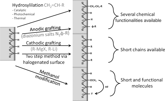
FIGURE 11.2 Schematic illustration and summary of the chemical modification pathways described in this chapter for monolayer functionalization of atomically flat Si–H (111).
11.2 TECHNIQUES CHARACTERIZING WET CHEMICALLY FUNCTIONALIZED SURFACES
As described in Chapter 2, reasonably well-established experimental techniques have been used for characterizing functionalized semiconductor surfaces. However, the information that can be derived from such techniques has not always been appreciated within the community, sometimes leading to overinterpretation. The goal of this section is therefore to critically discuss the main techniques typically used for understanding wet chemical surface functionalization, starting with spectroscopic techniques. In the end, it will be apparent that combining several techniques is important to gather the information necessary to guide the synthesis and to understand the self-assembly mechanisms.
11.2.1 X-Ray Photoelectron Spectroscopy
Detection of core levels of substrate atoms (Si, Ge, III–V), carbon atoms of the organic layer, head group atoms (N, O, S, etc.), and in some cases metal atoms can provide a quantitative measure of organic layer coverage and degree of chemical bonding. In particular, core level shifts can confirm the formation of interfacial Si–C bonds, the integrity of organic chain C–Hx bonds, and so on. In all reported work, XPS analysis is performed ex situ, that is, after transport of the sample in air from a glove box to the ultrahigh vacuum chamber. Issues associated with hydrocarbon contamination (adventitious carbon) on top of the organic layer and with contamination during evacuation of the load lock therefore need to be addressed since they can be serious in some cases (e.g., when the head group offers affinity to hydrocarbons, all surfaces contain adventitious carbon and oxygen traces). The main technical issues in the interpretation of the spectra revolve around the identification of impurities such as adventitious molecules containing carbon and oxygen, and the difficulty to detect and identify low-level oxidation of the substrate surface.
In the Si 2p region, it is also difficult to determine the surface stability just by studying the suboxides at the silicon surface. For instance, if a sample prepared in a glove box is quickly transferred to the vacuum chamber for XPS analysis, the surface may appear oxide free (i.e., stable), when in reality, it may not be thoroughly passivated and could oxidize further with time. In addition, the possible degradation of organic layers under intense X-ray irradiation by secondary electron emission must be checked by examining the time dependence of spectra.
The example of methyl-terminated silicon surfaces highlights the difficulty to get quantitative information just based on C 1s spectra, due to the contamination from the carbon atoms involved in the layer actually grafted on the surfaces. A low binding energy component (≈284.3 eV) has been attributed to photoelectrons from carbon atoms directly bonded to the silicon substrate. Methyl-terminated surfaces, which can be prepared from CH3MgX either by one-step anodic grafting or by two-step reaction via chlorination, exhibit varying amounts of adventitious carbons as determined by XPS (i.e., with C 1s peaks at energies higher than 285 eV) [47,48]. For instance, Fig. 11.3 shows the C 1s region of a freshly prepared SiCH3 surface (a) and after a 5 min annealing at 450°C (b), illustrating that physisorbed carbon species (contamination) can be removed by annealing [48,49].
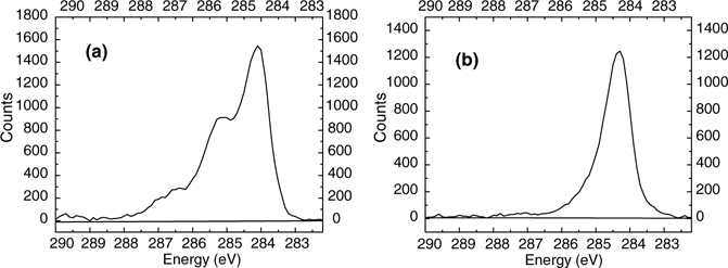
FIGURE 11.3 X-ray photoelectron spectra of the C 1s core level for methyl-terminated Si(111) surfaces prepared by anodic grafting of methylmagnesium according to the method presented in Section 11.4: (a) after rinsing in several solvents; (b) after annealing at 450°C in UHV for 5min. Only carbon atoms linked to silicon (Eb < 285 eV) are observed after annealing.
11.2.2 Infrared Absorption Spectroscopy
Several configurations are possible to perform IR spectroscopy. Much work has been done using multiple internal reflection (MIR) spectroscopy [50], where the organic layer is probed multiple times by the evanescent field. This configuration, which requires a special polishing of the edges, provides good sensitivity in a spectral range limited by the substrate absorption, and is particularly useful for polarization studies because all the components of the electric field are strong for typical internal angles (~45°) [51,52]. It is a powerful method to perform in situ studies on semiconductor liquid interfaces [53,54]. The main drawback for Si is that the spectral range is limited to frequencies above 900–1500 cm−1 depending on the sample length due to the substrate multiphonon absorption, which precludes the detection of Si–H bending vibrations (~620–650 cm−1) and makes difficult the detection of Si–O–Si bonds (~950–1200 cm−1). This geometry has therefore been successfully used mostly for characterizing Si–H, C–Hx, and C=O stretch modes [54].
A simple transmission geometry, typically performed at an incidence angle close to the Brewster angle [55], alleviates this problem and is ideal for in situ spectroscopy during measurements of the stability of organic layers in controlled gaseous environments as a function of temperature. However, good S/N is necessary when using transmission IR (TIR) spectroscopy because the IR beam interacts only once with the front and back of the sample [56]. Both MIR and TIR require double-side polished surfaces and take advantage of double-side functionalization.
An alternative to MIR that extends the spectral range and does not require double-side polished samples is an ATR technique whereby a Ge prism is brought in close contact with the surface under study (pressure needed) and an IR beam is internally reflected within the Ge prism. The semiconductor surface in close proximity is then probed by the evanescent field. In this configuration, the incidence angle within the Ge must be larger than sin−1(n1/n2), where n1 is the refraction index of the semiconductor under study (e.g., n1=3.45 for Si) and n2=4 is the refraction index of Ge. In general, θ ~ 65°, which is sufficient for n1 < 3.8. This configuration provides a substantial enhancement for the components of vibrations perpendicular to the interface [51,57]. Consequently, polarization studies are not well suited and some information is missing (or greatly suppressed) [27].
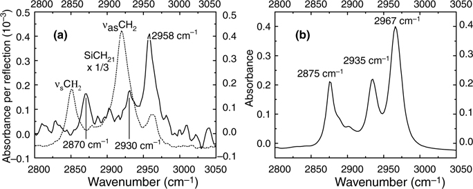
FIGURE 11.4 Infrared spectra in the vCH region of (a) Si–CH2–CH2–CH3 (solid line) and Si–C10H21 (dashed line) surfaces obtained by MIR and (b) liquid Cl3–Si–CH2–CH2–CH3 obtained in transmission.
An intrinsic limitation of IR spectroscopy is the need for a reference sample or surface. In contrast to all other spectroscopic techniques, the raw spectrum is a measure of the transmitted intensity and not the absorbed radiation. The absorption spectrum needs to be extracted using a reference sample with a similar bulk substrate and a controlled surface composition. This process is a source of difficulties. It is also difficult to distinguish contributions of the head groups and potential physisorbed molecules (source of adventitious carbon) because these species are not well oriented, hindering the usefulness of studies based on polarized radiation.
Besides technical issues with the choice of geometries, IR spectroscopy faces issues associated with interpretation and analysis. For instance, the assignment of the CHx region is not straightforward and can lead to errors, especially for short organic layers. In the case of nonfunctional alkyl chains, the CHx region is usually fit with four distinct bands, the asymmetric and symmetric modes of CH2 (Vas ≈ 2920 cm−1 and vs ~ 2850cm−1) and CH3 (Vas ≈ 2960 cm−1 and vs ≈ 2870 cm−1). In reality, this spectral region involves Fermi resonances of the overtones of the deformation modes of both CH2 and CH3, which need to be taken into account. The Fermi resonance requires the addition of a fifth component at ~2900 cm−1. This situation is further complicated by the fact that the manifestation of these Fermi resonances depends on the chain length! Calculations must be done to take into account these various effects.
To illustrate this issue, we consider here the case of the propyl chains (three carbons) attached to the silicon, Si–CH2–CH2–CH3. Figure 11.4a shows the infrared spectrum obtained by MIR in the vCH region for this surface (prepared from the propylmagnesium Grignard CH3–CH2–CH2—MgX). While this chain contains two CH2 groups in the alkyl chains, no IR bands appear around 2920 or 2850 cm−1, as is typically observed for a longer chain (SiC10H21, as shown with a dashed-line spectrum in Fig. 11.4a). This latter spectrum is consistent with the spectra of liquid trichloropropylsilane, Cl3–Si–CH2–CH2–CH3 (Fig. 11.4b). In particular, the shape of the bands has been well explained by calculations [58]. The origin of this dramatic difference between the short and long hydrocarbon chains lies squarely with the reduced role of Fermi resonance in the former case.
Another difficulty arises because the CHx stretch modes are often weak and undetectable. For instance, there has been no report of these modes on flat methoxylated surfaces until recently [59,60], although they had previously been observed in porous silicon [61]. In general, the 1250 cm−1 deformation mode of the methyl group is easier to identify and has therefore been utilized to characterize SAMs on flat surfaces [59,60,62].
11.2.3 Secondary Ion Mass Spectrometry
There have been few studies of monolayers adsorbed on semiconductors using secondary ion mass spectrometry (SIMS), partly because alkylsilane monolayers generate a limited set of low mass fragment ions that are not structurally significant [63,64]. This is because there is extensive cross-linking between the adsorbates, which leads to chain fragmentation during the SIMS process [63]. However, this is not the case for 1-alkene [65], 1-alkyne [65], 1-haloalkane [65], acid chloride [65,66], and alkanethiol [67,68] derived monolayers, in which a range of structurally significant fragments, and molecular and cluster ions are observed in the SIMS spectra.
SIMS is particularly useful to determine the monolayer adsorption sites that are difficult to identify with XPS. For example, XPS studies of Ga–S bonding in alkanethiolate SAMs adsorbed on GaAs(001) are complicated due to ambiguities in the spectra fitting in the relevant binding energy region and due to the weakness of the S 2p signal [69]. In contrast, SIMS does not suffer from such issues and is extremely surface sensitive. Thus, SIMS is an ideal technique to investigate adsorbate–substrate bonding. Using SIMS, McGuiness et al. [68] demonstrated that alkanethiols form direct S–(GaAs) attachments to bare GaAs(001) predominantly via As–S bonds with a small fraction of Ga–S bonds. SIMS has also been employed to characterize adsorbate–substrate bonding for monolayers prepared by scribing silicon under a series of 1-alkenes, 1-alkynes, and 1-haloalkanes [65,66]. However, SIMS does not always provide an unambiguous determination of the monolayer– substrate binding, as illustrated by the recent work of Arafat et al. [70] on 1-alkenes and 1-alkynes on silicon nitride substrates.
Since SIMS is able to provide surface-specific molecular chemical information with high lateral resolution, it has been employed to monitor both qualitatively and quantitatively reactions in monolayers [64,67,70,71]. SIMS is employed to follow not only the degradation reactions but also the functionalization of monolayers. For example, Arafat et al. [70] investigated the formation of amine-functionalized surfaces by reaction of acid-terminated monolayers using EDC/NHS chemistry. However, care must be taken in analyzing the resulting SIMS spectra and images because the chemical information obtained arises from the near-surface region (depth ~50 Å). Thus, SIMS may not provide information from the buried layers, such as in amine-functionalized monolayers.
11.2.4 Surface-Enhanced Raman Spectroscopy
Conventional Raman scattering is not sensitive enough to detect a single organic monolayer on atomically flat semiconductor surfaces. Typical modes associated with SAMs such as CHx, Si–C, and Si–O are not very strong Raman modes. On the other hand, it is possible to obtain Raman spectra in the case of porous silicon [41] or on flat silicon when nanoparticles (gold or silver) are adsorbed on top of SAM layers [72]. An example is shown in Fig. 11.5 for ~15 nm diameter gold particles attached on amino-terminated monolayers on Si surfaces. In this spectrum, the modes associated with δ(NH3+) are clearly seen. Similar bands have been observed in amino acids linked to metal (gold, silver) nanoparticles [73].
11.2.5 Spectroscopic Ellipsometry
Spectroscopic ellipsometry (SE) is a powerful method for fast and routine characterization of SAMs on semiconductors, yielding both the thickness and index of refraction, as recently reviewed by Hinrichs et al. [74]. Once calibrated, it provides a sensitive measure of the quality of the SAM layer and of the interface quality for gross interface modifications (e.g., oxidation). The main drawback is that it is highly model dependent and cannot therefore yield unambiguous parameters such as absolute thickness or precise dielectric function, particularly for inhomogeneous, imperfect layers. Consequently, SE is best used in conjunction with IR spectroscopy that provides more microscopic and chemical information.
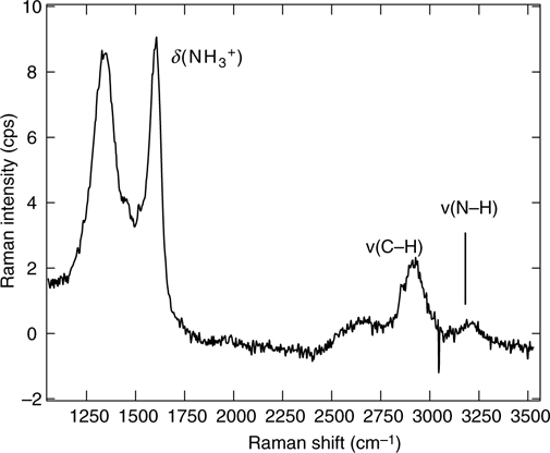
FIGURE 11.5 Raman spectra of amino-terminated silicon surface after deposition of gold nanoparticles.
11.2.6 X-Ray Reflectivity
Similarly to SE, X-ray reflectivity (XRR) provides an average measure of the entire surface, using standard Fresnel's equations. From these measurements, the height and surface roughness of the monolayer, the monolayer/silicon interface roughness, and the chain packing density can be extracted [75]. With XRR analysis, the entire surface of the sample is probed, while AFM and XPS look only at smaller parts of the surface. XRR is not readily able to measure the amount of oxidation that takes place, so other methods must be used to investigate this effect [76].
11.2.7 Contact Angle, Wettability
Contact angle (CA) measurements provide a convenient measure of the nature of SAM head groups. They are particularly useful to compare head groups with widely different hydrophilicities. The nature of functionalized surfaces ranges from highly hydrophilic surfaces (e.g., chemically prepared and hydrocarbon-free SiO2 surfaces) that give CA values close to zero (complete spreading of the drop) to highly hydrophobic surfaces (CA >110°) such as methyl-terminated long alkyl chain SAMs on oxide-free semiconductor surfaces.
The CA method provides an average value for SAM hydrophobicity, similarly to SE that provides an average value for the SAM index of refraction. Both methods therefore need to be coupled to chemically sensitive methods to deal with mixed or inhomogeneous SAMs.
11.2.8 Photoluminescence
The main advantage of photoluminescence is its high sensitivity to surface electronic states (i.e., recombination rates). It is therefore very valuable for applications that strongly depend on surface state densities, such as microelectronic-based sensors and photovoltaic devices. However, the nature of the defects cannot be extracted from such measurements without spectroscopy such as deep level transient spectroscopy (DLTS), inverse photoemission (IPES), and so on. Photoluminescence has been extensively used for porous Si because the PL level is very strong [41]. It is much weaker for flat silicon surfaces (partly due to nonradiative recombination of the generated electron–hole pairs) and has therefore not been used much. The nature of defects leading to nonradiative recombination is not well understood. Damage caused by the laser is also a potential problem that needs to be addressed. Nevertheless, there is detectable photoluminescence at 1130 nm on flat Si, which can be used as a sensitive probe of the electrical quality of the interface [77].
11.2.9 Electrical Measurements
Direct electrical tunneling measurements are probably the most sensitive technique for addressing the monolayer quality. Any defect will affect the transport from the substrate to the metal contact or vice versa. This method is robust and works well for reasonably good monolayers (i.e., with no shorts). The tunneling current is very sensitive to interface defects, although as for photoluminescence, the nature of these defects is not well known. They are thought to involve structural defects, dangling bonds, pinhole, oxidation, and other chemical impurities.
This technique is not widely used because it requires non-damaging and reliable metal deposition to establish contacts. Metal evaporation can indeed damage the organic layer. Currently, one of the most reliable methods is the use of Hg top contact [78,79]. A recent review article addresses in detail the different issues associated with metal deposition for contact formation (monolayer properties, junction, semiconductor doping, etc.) in such systems [80].
11.2.10 Imaging Techniques
Atomic force microscopy is primarily used to measure the morphology of the surface after chemical modification to determine whether additional roughness is introduced in the process (due to oxidation, for instance) or whether the organic layer is homogeneous on a 0.1 nm scale. For short SAMs, the surface roughness remains, in general, close to that of the starting surface while for large molecules or long-chain molecules additional roughness is typically observed. For instance, indication of DNA hybridization [81] or changes of orientation of grafted azobenzene [82] have been observed with AFM.
For any tip-based technique, there is a possibility that the tip can interact with the SAM so that some organic molecules can bind to it. The nature of the head group must therefore be kept in mind when doing AFM since the affinity of the surface toward the tip depends on the head group. The ability of the head groups to interact with the tip can also be used to pattern surfaces [83]. As summarized in several review articles [43,84], there are different ways to perform lithography of self-assembled monolayers using AFM tips, including local electrochemistry to remove part of the layers through anodization [85] or to graft molecules on small area through cathodic process [86].
Scanning tunneling microscopy (STM) is harder to perform on thick organic layers but has been used successfully on as-prepared H-terminated Si surfaces [45,87], or after modification with short organic molecules such as –CH3 [88] or –C6H4R [45].
11.2.11 Electron and Atom Diffraction Methods
Low-energy electron diffraction is usually very sensitive to surface reconstruction, as demonstrated in thousands of surface science experiments under ultrahigh vacuum conditions. However, care must be taken in the interpretation of LEED patterns obtained for organic layers grafted to unreconstructed H-terminated Si surfaces. The observation of a sharp (1×1) pattern does not necessarily mean that a perfect surface termination has been established because the sensitivity to a thin adlayer composed primarily of carbon and hydrogen is poor if the substrate remains unreconstructed.
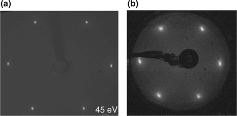
FIGURE 11.6 (a) LEED pattern presented in Ref. 37. (b) LEED pattern obtained at 37.7 eV on 1/3 SiOCH3, 2/3 SiH.
This is illustrated in Fig. 11.6a, which shows the LEED pattern observed for an unreconstructed Si(111)-(1×1) surface covered with a very homogeneous layer of methoxy molecules (each surrounded by six H atoms) arranged in a √(3) × √(3) pattern [60]. This pattern is identical to the (1×1) pattern obtained for the starting unreconstructed surface (completely monohydride terminated and atomically flat), and with the (1×1) pattern reported for a CH3-covered, atomically flat Si(111) surface [48]. If hydrogen is removed from a H/Si(111)-(1×1) surface by beam methods, the top surface begins to reconstruct and the LEED pattern is affected as shown in Fig. 11.6b.
This example illustrates that, unless the top Si layer is reconstructed, it is not possible to conclude from a (1×1) LEED pattern that the organic overlayer is perfectly ordered and continuous.
A much more appropriate method to determine the homogeneity of an organic layer is He diffraction, as nicely illustrated by Scoles for self-assembled monolayers of alkanethiol on gold [89].
In conclusion for this methods section, it is clear that a combination of spectroscopy, imaging, electrical, and diffraction methods is needed to characterize the nature of functionalized semiconductor surfaces. In doing so, the information derived from each technique needs to be examined critically.
11.3 HYDROSILYLATION OF H-TERMINATED SURFACES
Since the main emphasis of this chapter is on the functionalization of H-terminated surfaces, in particular silicon surfaces, it is most appropriate to start with hydrosilylation, which is a well-known reaction in inorganic chemistry describing an addition of organic silicon hydride compounds to species with multiple bonds, particularly C–C, C–O, or C–N [90,91].
The essential element of hydrosilylation, summarized in Equation 11.1, is the activation of the alkene, alkyne, or other unsaturated carbon compounds to permit reaction with the Si–H surface. The three main forms of activation on surfaces include the use of catalysts or Lewis acids, UV light, and temperature. The last two methods of activation involve a surface reaction and consequently are not derived from homogeneous hydrosilylation in solution that relies on a catalyst. The surface reaction can be written as
For the attachment of alkyl chains to H-terminated silicon surfaces, the hydrosilylation mechanism provides an effective means of forming a strong Si–C bond between Si and alkyl chain molecules, starting with alkene or alkyne reagents. The resulting SAMs are both thermodynamically and kinetically stable due to the high bond strength and low polarity of the Si–C bond. The main requirements for this wet chemical process are that (i) the molecules remain liquid (hence some restriction on their length) and stable under the reaction conditions, and (ii) their functional groups be less reactive with the Si–H surface than with the targeted functions (alkene or alkyne termination). These requirements lead to two strategies: (1) protection of the functional groups during reaction (with subsequent deprotection to regain functionality), which often requires the synthesis of such protected species since they are not available commercially, and (2) further modification of the grafted molecules without degradation of the initial Si/SAM interface (i.e., mild conditions are necessary to avoid silicon oxidation or other unwanted interface reactions).
11.3.1 Catalyst-Aided Reactions
In homogeneous media (solution), catalytic hydrosilylation processes are commonly used. Such reactions can occur either by creation of a radical [90] or by polarization of the bond under consideration (predominant in most systems). The catalysts used may be transition metal complexes, nucleophiles (e.g., tertiary amine), or Lewis acids (AlCl3, EtAlCl2) [92–94]. The hydrosilylation process catalyzed by transition metal complexes was first proposed by Chalk and Harrod in 1965 as illustrated in Fig. 11.7 [92], and then expanded by using EtAlCl2 (Fig. 11.8) and peroxides as shown in Fig. 11.9.
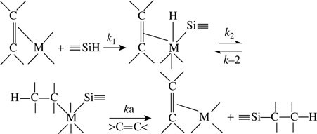
FIGURE 11.7 Mechanism proposed by Chalk and Harrod for the hydrosilylation of olefins catalyzed by group VIII metal complexes [92].
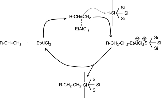
FIGURE 11.8 Schematic representation of the hydrosilylation mechanism using EtAlCl2 to catalyze the organosilicon reaction.
Similar reactions have been performed on surfaces, initially on H-terminated porous silicon. Palladium-, rhodium-, or platinum-based catalysts have been used on surfaces but the process often leads to oxidation and metal reduction as thoroughly reviewed by Buriak [44] and Boukherroub and Szunerits [41].
In contrast, Lewis acid-catalyzed or -mediated hydrosilylation works very well to functionalize porous silicon. A catalyst of choice has been EtAlCl2 because it is soluble in nonpolar solvents. It was first demonstrated by Boukherroub et al. and has been used extensively to functionalize porous and flat silicon surfaces [95,96]. The mechanism is shown in Fig. 11.8, and follows the pathways determined by standard organosilicon chemistry [93].
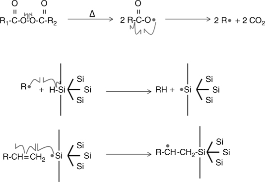
FIGURE 11.9 Schematic representation of the hydrosilylation mechanism using a peroxide agent to initiate a radical reaction.
The first example of functionalization of H-terminated Si surfaces by organic molecules was performed using radical initiators, such as diacyl peroxides [97]. Such catalysts are known to create radicals to initiate a chain reaction in polymers, for instance, and have been used early to perform hydrosilylation in organic chemistry [90]. When heated, the initiator undergoes homolytic cleavage to form acyloxy radicals that further decompose into carbon dioxide and an alkyl radical. The alkyl radical abstracts H• from a Si–H surface to produce a silicon radical on the surface. Such a coordinatively unsaturated “dangling bond” is known to react extremely rapidly with olefins that are in close proximity. The formation of a silicon–Carbon bond (olefin attachment) is therefore the favorable next step. The resulting carbon-based radical is stabilized by abstracting a hydrogen atom either from the allylic position of an unreacted olefin or from a neighboring Si–H group. This method therefore often leads to a chain reaction on the surface. This mechanism and its associated reaction kinetics have been examined, confirmed, and quantified by first-principles calculations [98].
Hydride abstraction initiated hydrosilylation via an ionic pathway has also been proposed, using for instance triphenylcarbenium cations (Fig. 11.10) [99]. The cation is supposed to remove H− from the surface, producing a positive charge on the silicon a surface leading to a nucleophilic attack by the electron-rich double bond. Such a process leads to Si–C formation and a β-silyl-substituted carbocation that can propagate the reaction by abstracting the hydrogen nearby.
In 2005, Arafat et al. used 4-(decanoate)-2,2,6,6-tetramethylpiperidinooxy (TEMPO) as a radical initiator to graft nonfunctional alkenes such as octade-cene [100] or even unprotected carboxylic acids to Si(111) surfaces [101]. This approach is of particular interest because it makes it possible to attach directly organic layers with functional groups on silicon surfaces.
The hydrosilylation reaction can also be performed without any catalyst, if another activating medium (e.g., appropriate photons or thermal energy or electrochemistry activation) is used, as described in the following sections.
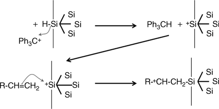
FIGURE 11.10 Schematic representation of the hydrosilylation mechanism using a carbocation to initiate an ionic reaction.
11.3.2 Photochemically Induced Reactions
The initial concept behind photoactivation of H-terminated surfaces was that photons with energy larger than the Si–H bond energy (~3.5 eV) could directly break this bond to form a silicon radical, thus activating the surface. Such a process would therefore require wavelengths shorter than 350 nm (3.55 eV). Clearly, highly anhydrous solutions (with the appropriate alkene) are required since silicon radicals strongly react with water to form silicon oxide. This simple picture motivated the pioneering work of Terry et al. [102]. His group used XPS to show that organic monolayers could be formed on silicon by illumination of freshly prepared Si–H surfaces in liquid pentene for 2 h with a mercury lamp (λ=185 and 253.7 nm) [102]. They later grafted several other alkene and alkyne molecules using a variety of wavelengths and pointed out that silicon oxidation occurs in the presence of oxygen when wavelengths shorter than 350 nm are used [40]. Such observations support the idea that the first step could be an activation of the surface mediated by breaking Si–H bonds at short wavelengths. The reactive radical formed on the surface would then react, similarly to the radical obtained via the use of a radical, either with an oxidizing species leading to silicon oxidation or with a double bond leading to covalent grafting. The cross section for direct Si–H bond breakage is, however, very low for isolated Si–H (e.g., H-terminated surfaces in vacuum). The role of the solvent and the potential cooperative effects of the organic molecules are therefore critical for this mechanism.
Over the past decade, photochemical grafting of various alkene-based organic molecules has been performed using a wide range of photon energies [103,104], including energies that are lower than the Si–H bond energy and even than the substrate bandgap. Since the photon energy used in these studies is significantly lower than the energy necessary to induce homolytic bond cleavage, it has been suggested that photoexcitation of substrate charges is likely responsible for the generation of active sites on the Si surface. The effectiveness of photons with energies below the Si–H bond energy (3.5 eV) indicates that mechanisms other than the simple mechanism outlined above may be operational [103]. In 2001, a mechanism involving the generation of excitons in the substrate was proposed by Stewart and Buriak to account for the observed wavelength dependence [105]. The main idea is the creation of electrons and holes in the substrate, which are then available to initiate the reaction and the nucleophilic attack from the electron-rich C=C. Both mechanisms are illustrated in Fig. 11.11.
This electron-hole generation mechanism was further corroborated by using two model surfaces with Si–H bonds grafted directly on either (i) an oxide-free Si or (ii) an oxidized surface as shown in Fig. 11.12. The observation of hydrosilylation only on oxide-free surfaces suggests that electron-hole pair excitons are important for the mechanism of UV-induced surface hydrosilylation [106].
Another contribution to surface reactions on H-terminated Si surfaces, involving chain reaction, has been suggested in several studies. Even if an excitonic process is at the origin of the grafting process, the propagation of functionalization may still involve radicals. The effect of a radical on the reaction of the neighboring Si–H site was first observed in ultrahigh vacuum by STM [107]. Confirmation of this mechanism in liquid environment is more difficult. Miramond and Vuillaume have shown that such surface reactions are influenced by the substrate doping although short wavelengths (257 nm) were still used in this work [108]. Grafting of highly n-doped silicon, for instance, led to the formation of more disordered monolayers that therefore exhibited larger leakage current densities (>10−4A/cm2 compared to 10−7 A/cm2 for others) when embedded in a silicon/monolayer/metal junction.
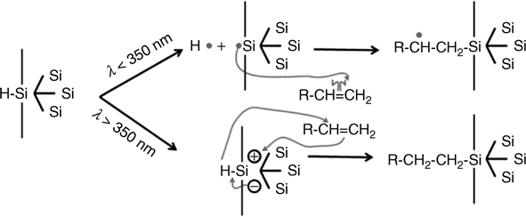
FIGURE 11.11 Schematic illustration of the two pathways for photochemically induced reactions for hydrosilylation of H-terminated Si surfaces: (top) radical-based mechanism; (bottom) exciton-based mechanism.
For completeness, we note that functionalization of other substrates, such as GaN, has been achieved by using this photochemical method [109].
Yet another fundamentally different mechanism has been suggested in the past few years by Hamers and coworkers. The observation of hydrosilylation reaction on H-terminated diamond or amorphous carbon using UV light with energies lower than the bandgap energy (e.g., 254 nm for reaction on diamond) [110] was used as evidence that the exciton model may not always be dominant. Instead, it was proposed that photoemission of electrons into the liquid was responsible for producing radicals on acceptor molecules that could then catalyze the hydrosilylation of H-terminated carbon surfaces. The concept was subsequently carried over to silicon substrates [111], although an unambiguous confirmation is difficult to obtain.
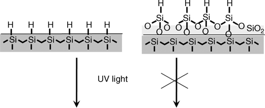
FIGURE 11.12 Schematic representation of the two model surfaces: (left) atomically flat, oxide-free H-terminated Si(111) surface; (right) oxidized Si functionalized with trichloroailane, resulting in a H-terminated oxide surface.
No matter what the detailed mechanism is, the photochemical method brings two important advantages for functionalizing semiconductor surfaces. First, alkene molecules can be grafted with a variety of functional groups because surface radicals can be formed (in some fashion), thus enhancing the reaction with alkene groups over that with functional groups, such as carboxylic acid [112], ester [113], activated ester [114], or other molecules with available C–C multiple bonds [82]. Second, the method is ideal to use optical lithography to pattern the SAMs and form molecular arrays [115,116]. Recently, optical lithography has been applied, for instance, to process organic monolayers on oxide-free silicon substrates by using a photothermal laser at 514 nm [117].
11.3.3 Thermally Activated Reactions
Thermal activation of hydrosilylation reactions is a straightforward and interesting alternative to chemical or photochemical activation. This procedure typically involves immersing the H-terminated Si surfaces in an anhydrous solution of appropriate alkenes for extended periods of time (from hours to days) at moderate temperatures (from 150 to 200°C). The process can be well modeled by standard surface chemistry, whereby Si–H reacts with an alkene group through a transition state involving Si · · · C(1)–H and Si–H · · · C(2)H2, which results in the formation of Si–C(1)H2–C(2)H3– · · ·. Although this thermal process is sensitive to impurities because it is slow, there is an intrinsic advantage to the method that has not been fully appreciated. The higher solution temperatures typically used for such processing facilitate the removal of trace water, thus reducing the potential risk of surface oxidation. Therefore, simple methods and care in the execution of experiments make it possible to obtain surfaces with negligible interface oxide and high PL intensities (similar to H-terminated Si surfaces) [118]. Such surfaces are significantly more stable than H-terminated surfaces once produced because of the protective SAM layer, even if the majority of the surface (e.g., 60–70%) is still H-terminated.
Thermal grafting also provides an “annealing effect” on the substrate. Such annealing can help to suppress a degradation of the functionalization process due to the compensating effect present on p-type Si surfaces arising from the polishing process [119]. These subtle effects are important because they ultimately limit the performance of actual devices based on the hydrosilylation process. Thermal processing constitutes a practical means of circumventing these issues.
Chidsey and coworkers first performed thermal hydrosilylation in the early 1990s [97,120]. The method and the quality of the monolayers have since been improved by Sieval by using several solvents and unsaturated molecules [121]. Such reactions were initially thought to involve surface radicals similar to those generated by catalysts or photochemical activation (λ < 350 nm) [44,122]. It was also proposed that the first step of initiation was due to traces of water, oxygen, or other impurities [122,123]. A similar mechanism has recently been suggested for homogeneous hydrosilylation in solution, in which air could activate Si–H bonds instead of catalysts [124]. However, it is not clear how homolytic cleavage of a strong Si–H bond with bond energies on the order of 80–90 kcal/mol could occur at an appreciable rate at a temperature as low as 150°C. A more concerted mechanism was therefore proposed [41] and DFT calculations performed, as illustrated in Fig. 11.13 [125].
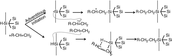
FIGURE 11.13 Possible reaction pathways for the thermal hydrosilylation: (top) radical-based mechanism; (bottom) concerted mechanism.
Recent studies based on thermal activation have highlighted the differences between the grafting of alkenes and alkynes on flat silicon surfaces. By using a mixed solution of alkene and alkyne or a molecule containing both an alkyne at one end and an alkene at the other, it was shown that triple bonds are preferentially attached over double bonds [126]. Furthermore, Scheres et al. have confirmed that an increased surface coverage is obtained with alkenyl chains on silicon, compared to what can be achieved with alkyl chains [127]. Interestingly, in addition to the classical thermal method [122], alkynes have also been grafted by very mild, room-temperature methods in the dark [128], producing better quality surfaces than alkenes [129].
The thermal grafting methods have been avoided partly for fear that thermal energy may activate the functional groups and induce them to react with SiH. Despite this potential problem, high-quality acid-terminated surfaces have been prepared by thermal grafting [130–132]. Carboxylic acid groups can then be modified and used for several applications such as metal deposition [130], biosensors [81,132], electrical contacts [79,133], or deposition of nanoparticles [131].
Practically, thermal grafting represents the most direct and easiest way to graft organic layers on surfaces. There is no need for special equipment or procedure such as UV light reactors, electrochemical cells, or addition of catalysts. The only requirement is hermetically closed glassware that can be purged with argon. There is no constraint on the geometry, which makes it possible to prepare samples of any size. Functionalization occurs on both sides and over large areas, which is not as easy for UV grafting at 254 nm, for instance, since quartz is required. A simple hot plate is sufficient to shake the solution when necessary, for example, in the case of mixed alkene molecules. To prepare mixed monolayers, temperature is an important parameter to control the composition because temperature and convection usually affect the surface reaction differently for each component of the mixture.
11.4 ELECTROCHEMISTRY OF H-TERMINATED SURFACES
Electrochemistry is naturally well suited to induce modification of H-terminated Si surfaces because holes or electrons have clearly been shown to induce hydrosilylation reactions. While many side or chain reactions can also occur, it is easiest and best to focus initially on the injection of holes or electrons into acceptor or donor molecules or groups that can then provide radicals as discussed below.
11.4.1 Cathodic Grafting
In cathodic grafting, an electron is created in the silicon substrate and can be captured by an acceptor species, such as the azo group (|N≡N+–) of diazonium salts, as illustrated in Fig. 11.14. This process releases dinitrogen, thus producing an aryl radical [134]. Although diazonium salts are most commonly used, many other molecules can undergo the same process to become a radical. For instance, aryliodonium salts have been successfully grafted onto SiH [135]. Other halogeno-alkanes of the form X–R, where X is a halogen, can also be reacted using this cathodic method because the halogen atom preferentially attracts the substrate electron to form X− ions, thus releasing a radical R• [136].
Once formed, the radical can then abstract a hydrogen atom from the ≡SiH surface, producing ≡Si• that can easily recombine with many molecules, and in particular other radicals nearby. Since the functional group R can be tailored to a required functionality (e.g., R=Br, NO2, COOH, CN, or CnH2n+1 for n = 1,4, 12), this method is useful to functionalize surfaces without formation of silicon oxide [137].
The main advantage of cathodic grafting is that it brings electrons to the surface, making it more resistant to nucleophilic attack by water and therefore to oxidation. A common problem, however, is the ease with which the salt radicals can polymerize. The challenge for such a procedure is therefore to control unwanted polymerization. This functionalization has also been applied to other surfaces such as GaAs or Pd [138].
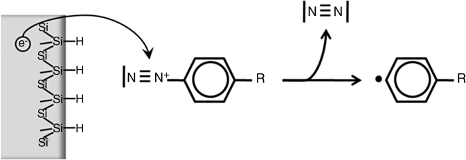
FIGURE 11.14 Radicalization of a diazonium salt by electron capture by the azo group: R can be Br, NO2, COOH, CN, or CnH2n+1 (n = 1, 4, 12).
11.4.2 Anodic Grafting
The anodic generation of an organic radical R• is shown schematically in Fig. 11.15. Once formed, the radical can react with the H-terminated surface, thus leading to hydrogen abstraction. A second radical may then be grafted on the remaining silicon dangling bond. This mechanism is similar to the exciton mechanism in the photochemical grafting described later in this section, whereby holes interact directly with the ≡SiH surface, leading to the formation of a radical ≡Si•.
Anodization of silicon surfaces by releasing a hole at the surface (or driving an electron deep in the substrate) unavoidably leads to formation of a layer of silicon oxide in the presence of water or, in the case of fluoride electrolytes, to the dissolution of silicon. If an organic modification is desired, it is therefore very important to operate under rigorously anhydrous conditions.
Whatever the dominant path may be, it is likely that the radical species R• and ≡Si• are both present, since there is an equilibrium formed usually written as
![]()
Anodic grafting has been explored for alkyl, alkenyl, alkynyl, and aryl radicals using, for instance, Grignard electrolytes, and also for halogeno and cyano radicals using anhydrous acetonitrile electrolytes. Rapid grafting is generally obtained. However, the reaction is self-limiting only for the most inert radicals such as alkyl and ethynyl. For more reactive radicals, such as halogeno or cyano salts, side reactions may be observed, such as electropolymerization on the silicon surface, for example. Grignards are especially attractive precursors, since they ideally ensure anhydrous conditions by neutralizing trace amounts of water molecules and also constitute the electrolyte [139]. They are typically available with a variety of aliphatic and aromatic groups. There are, however, some restrictions on the type of possible substituents due to the high reactivity of the Grignard reagents with protonic molecules, that dissociate H+ typically bound to nitrogen or oxygen [140].
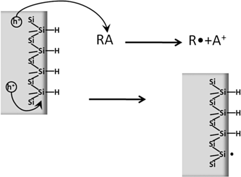
FIGURE 11.15 Possible pathways involving the radicalization of electron-donor species to initiate the anodic grafting of organic molecules: (top) ionization of molecule in solution; (bottom) ionization of surface Si atom.
For completeness, we note that Grignard grafting on H-terminated Si surfaces can also occur simply by immersion of a H/Si sample in an organomagnesium (RMgX) solution at room temperature on porous silicon [95,141] or at 85°C during 16 h on flat silicon [95]. On atomically rough surfaces or in porous silicon, it appears that the mechanism involves the cleavage and reaction of Si–Si back-bonds without net consumption of SiH [41,141]. On flat silicon, for which Si–Si bond breaking is energetically more costly due to strain, the modification associated with the consumption of Si–H remains surprising.
11.5 USE OF HALOGEN-TERMINATED SURFACES
A two-step procedure has been shown to facilitate this process. In the first step, the surface hydrogen is replaced by a halogen (typically chlorine). Once the surface is halogenated, the second step involves immersion in Grignard or organolithium solutions. The reaction that follows is typical of a classical Wurtz coupling described in inorganic chemistry and schematically shown in Fig. 11.16. In this reaction, the carbon linked to the magnesium has a nucleophilic character and thus reacts with the partially positively charged carbon atom linked to a halogen atom, releasing a longer alkane and a Mg halide.
A halogenated silicon atom behaves in a manner similar to the carbon atom in a halogenoalkane, namely, it reacts with the Grignard reagent to graft the organic ligand, releasing a transition metal halide as schematically shown in Fig. 11.17.
This two-step method was pioneered by Bansal and Lewis to attach organic monolayers on Cl-terminated silicon surfaces with Grignard reagents [142]. The method was improved to functionalize surfaces with low densities of electronic defects [143]. The exact mechanism involved in the two steps has been investigated in the past few years [62,144]. Using this two-step method with electrochemistry, well-defined methyl-terminated surfaces have been obtained with high coverages [48].
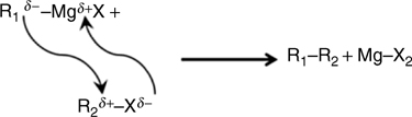
FIGURE 11.16 Mechanism of the Wurtz reaction between an organomagnesium R1MgX and an organohalide R2X [140].
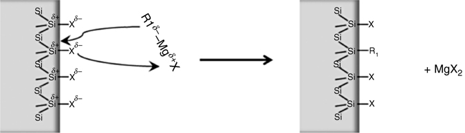
FIGURE 11.17 Possible mechanism of the reaction of an organomagnesium R1MgX and a surface silicon halide Si–X.
In considering the quality of surfaces functionalized using the two-step process, it is important to understand the first step, or halogenation of H-terminated silicon surfaces. Chlorination, for instance, can be achieved in two ways on silicon surfaces:
- wet chemical process using PCl5 (with benzoyl peroxide as a radical initiator in chlorobenzene or with UV);
- gas-phase process using Cl2 gas at moderate temperatures.
Both methods can remove the hydrogen layer completely, as evidenced by the complete loss of Si–H stretch modes, and replace it with a chlorine layer without etching the silicon substrate, as determined by results on atomically flat H-terminated silicon surfaces [145]. In the case of gas-phase Cl2, the reaction can be followed as a function of treatment time, confirming that chlorine substitutionally replaces hydrogen, leading to a newly observed blue shift of the remaining Si–H neighbors [146,147].
The stability of chlorine-terminated silicon surfaces has been examined. Similarly to H-terminated surfaces, Cl-terminated Si surfaces are stable in water vapor. Despite early claims [148], this stability makes it impossible to form hydroxyl-terminated surfaces starting from Cl-terminated surfaces because water can only react with Si–Cl at temperatures (~300°C) at which Si–OH is not stable, leading to the incorporation of oxygen into the silicon lattice (i.e., oxidation) [145]. Once oxidized, the surface can of course support hydroxyl groups, hence the erroneous interpretation [148].
Chlorination of germanium surfaces is straightforward as well, thus making Ge amenable to Grignard chemistry. In addition to the methods developed for Si, chlorination of Ge surfaces can be achieved by immersion in hydrochloric acid [23]. Attachment of organic layers on chlorinated germanium was performed with similar procedures, such as ethylation [149] or alkane-linked Ge–S–C bonds obtained from alkanethiol [150]. However, in most cases, the stability of functionalized Ge surfaces has not been studied or demonstrated. Much needs to be done in this respect to fully assess the value of Ge-based hybrid systems. This procedure has also been applied to several III–V semiconductors, including Ga–P [151].
In closing, we note that halogens other than chlorine, particularly iodine and bromine, have been attached on H-terminated silicon surfaces. Following methods to brominate hydrosilanes in liquid phase [152], Br-terminated surfaces have been obtained [153], using N-bromosuccinimide (NBS) in DMF for 20min at 60°C in the presence of benzoyl peroxide as the radical initiator. Alternatively, neat CCl3Br can be used under thermal conditions (80°C for 30 min), with photolysis (300 nm UV for 20 min), or in the presence of benzoyl peroxide (60°C for 30 min) [153].
Iodination has been performed on porous silicon as reviewed by Boukherroub and Szunerits [41]. In this case, it appears that the reaction of the iodine gas involves the breaking of Si–Si bonds instead of Si–H bonds. In order to attack Si–H directly and to thus perfect a procedure that can be reliably used for modifying flat Si–H, iodination of silicon surfaces was carried out using iodoform (CHI3) under visible light or thermal activation [154]. It was postulated that iodine radicals can be generated by light or heat activation, leading to a direct reaction with Si–H. Cai et al. used iodine dissolved in benzene, for instance, as a way to increase the Si–I coverage on flat surfaces [115].
Figure 11.18 summarizes the various methods developed for halogenating H-terminated silicon surfaces. Interestingly, it has not been possible to replace hydrogen by fluorine, mostly because fluorinated liquid leads to hydrogen termination [30] and because gas-phase fluorine is very aggressive, leading to strong etching [155]. This difficulty in obtaining fluorinated silicon surfaces has motivated the work described in the next section, where a very recent method for partial fluorination of H-terminated silicon surfaces is presented. This method opens new possibilities for enhanced functionalization of silicon surfaces.
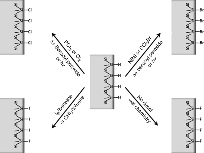
FIGURE 11.18 Halogenated flat, H-terminated silicon surfaces by wet chemistry.
11.6 ALCOHOL REACTION WITH H-TERMINATED SI SURFACES
Chapter 12 is concerned with the stability of functionalized surfaces. Here, we focus on the reaction of alcohols (mostly methanol) with atomically flat, monohydride-terminated Si(111) surfaces. Indeed, the structure of the surface is shown to play an important role in both the degree of reaction and the properties of the functionalized surfaces.
It has been well established that immersion of H-terminated Si surfaces in alcohols leads to the grafting of alkoxy groups on Si surfaces, such as methoxy for methanol, forming Si–O–C linking bonds. The reaction can be thermally [156,157] or photochemically induced [154,158,159], as described above for standard hydrosilylation, but has also been observed to take place at room temperature after long immersion times (~2–3 days), clearly ruling out the need for radical formation [160]. In fact, the preparation of monolayers linked via Si–O–C bonds to silicon surfaces has typically been achieved under mild conditions. As recently suggested by Shirahata using contact angle measurements [159], even long-chain alcohols can be grafted at 40°C, conditions under which alkene cannot be attached. The use of such mild conditions ensures that the functional groups of the grafted molecules remain intact [161,162]. Alternatively, Zhu developed a two-step method to graft long-chain alcohols at 70°C, involving an intermediate Si–Cl surface [163], and extended this approach to attach polyethylene glycol species [164].
In most of these studies performed over the last decade, there is typically a small amount of interface oxide generated during the reaction as revealed by XPS or IR spectroscopic studies [154,163,165]. Furthermore, AFM investigations have also shown that pitting occurs on initially flat H-terminated Si(111) surfaces during the grafting of alcohol species in addition to some partial oxidation [157,166]. Nonetheless, 1-decanol has been successfully grafted on Si(111) with little detectable silicon oxide at the interface [162,167].
These two types of defects, oxidation and pitting, have undermined the potential of grafting alcohols on silicon surfaces. Pitting can be partially understood by invoking mechanisms proposed to address thermal grafting on porous silicon, such as Si–Si bond breaking during reaction with alcohols leading to subsequent etching of silicon [41,168]. Oxidation, on the other hand, is most likely due to trace amounts of water in the alcohol solution, due to the high affinity of water to the OH group of alcohols (which is not the case for alkene molecules, for instance). To reduce the concentration of unwanted water, Boukherroub et al. suggested adding chlorotri-methylsilane to the reaction mixture to scavenge undesirable nucleophiles during wet chemical modification of Si(111)–H [157]. The use of highly anhydrous chemicals was also attempted, but until recently, some oxidation of the silicon could not be avoided during methanol reaction with H-terminated Si surfaces, even though the majority of the surface could clearly be perfectly methoxylated [160,169].
The recent finding that immersion of H-terminated Si(111) surfaces in neat anhydrous methanol at 70°C inside a nitrogen-purged glove box leads to the formation of oxide-free methoxy-terminated surfaces [59,60] confirms the role of trace amount of water in oxidizing the surface during alcohol reactions and highlights the importance of moderately elevated temperatures to reduce trace water contamination. Processing at this temperature also brings an unexpected result, namely, that only 1/3 of a monolayer can be reacted, the other 2/3 of the surface remaining hydrogen terminated. The resulting surface, schematically represented in Fig. 11.19, is composed of methoxy centers surrounded by six surface Si–H. The reason for this arrangement, as recently described and supported theoretically [60], is that once adsorbed, the methoxy group rotates around its axis, thus protecting the surrounding Si–H groups (Fig. 11.20). This effect is more pronounced at 70°C, and results in the formation of nanopatterned surfaces [60].
The fact that the surface remains atomically flat and oxide free after methoxylation provides a very special template for subsequent chemical reactions. For instance, immersion of such a methoxylated surface in HF produces a partially fluorine-terminated surface, that is, each methoxy group is replaced by fluorine, with no changes in the surrounding Si–H groups and no attack of Si–Si bonds (i.e., no pitting). The surface remains atomically flat, as can be seen for the reaction mechanism shown in Fig. 11.20. Once fluorinated, the surface can be hydroxylated by simple immersion in water. Again, only the Si–F bonds are attacked, not the surrounding Si–H groups or the Si–Si back-bonds. The process can be repeated multiple times, resulting in fluorine attachment by immersion in hydrofluoric acid and hydroxyl replacement of F by immersion in water, without affecting the ~2/3 monolayer H coverage.
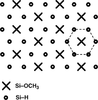
FIGURE 11.19 Schematic representation of the partially methoxylated Si(111) surface after reaction with methanol.
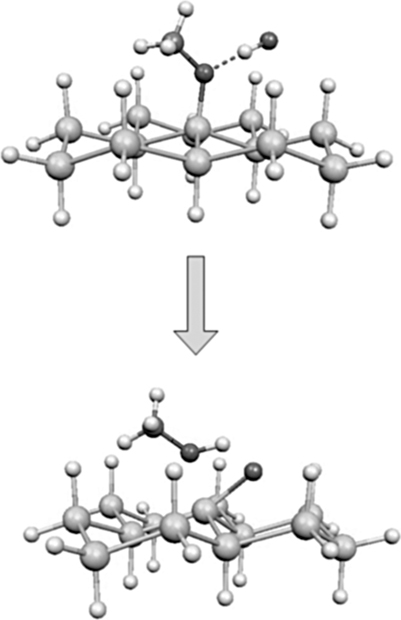
FIGURE 11.20 Theoretically calculated reaction of HF with methoxy-terminated silicon in an atomically flat surface with six Si–H species surrounding the methoxy.
The formation of a partially hydroxylated surface on an otherwise oxide-free surface opens up a host of possibilities, in particular for atomic layer deposition of high and low k dielectrics. For instance, HfO2 and dimethyl-SiH have been deposited on oxide-free silicon [60]. In general, the presence of isolated OH groups on an otherwise hydrophobic (H-terminated) surface is of great value to attach molecules (e.g. phosphonates) that usually could only functionalize oxidized surfaces, which is of interest for silicon-based biosensors, for instance [170].
The fundamental mechanism for the above chemistry is determined by the structural and chemical perfection of the surface. Indeed, if there is any detectable oxide on the surface (characterized by interface atomic roughness), immersion in HF leads to H termination of the surface in the oxidized areas. This observation underscores the fact that the interface between crystalline silicon and amorphous SiO2 is not atomically smooth. The mechanism for HF etching described at the beginning of this chapter is in fact only valid because the interface is rough. Figure 11.21 schematically illustrates this point. On the left, the fluorinated surface can be further attacked by HF to form a H-terminated surface. On the right, an atomically smooth and partially fluorinated surface cannot be further attacked, thus remaining fluorinated.
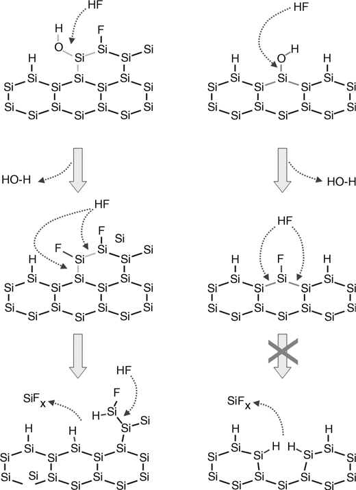
FIGURE 11.21 Schematic mechanism of HF attack on a rough fluorinated Si surface (left) and on an atomically smooth partially fluorinated Si surface (right).
In general, alkoxy termination of H-terminated surfaces is possible, as described in more detail in the next chapter, but the special properties of atomically flat surfaces critically hinge on the ability to avoid oxidation. Thermal processing appears to be a convenient method to prepare oxide-free surfaces, and is required to produce highly uniform nanopatterned surfaces.
Atomically flat and partially methoxy-terminated surfaces provide a model system to test a variety of physical phenomena such as vibrational and electronic dynamics, chemical reactions such as snap on chemistry, and chemical stability (e.g., increased stability of Si–H when surrounded by F). For instance, an unusual blue shift of the Si–H stretch mode in the vicinity of a halogen observed for chlorine [146] was recently explained theoretically and shown to lead to Si–H stabilization [147]. The ability to fluorinate a surface in a homogeneous nanopattern has made it possible to distinguish among several mechanisms, for instance [146,147]. These surfaces are also a model system to test the interaction of electron, photon, atoms, and ions with a variety of atoms or molecules on unreconstructed surfaces. An example was given for LEED in the experimental section and it is anticipated that further work will be done using He scattering, scanning tunneling microscopy, grazing incidence X-ray scattering, and other methods.
11.7 OUTLOOK
The work summarized in this chapter underscores the importance of wet chemical methods for semiconductor surface functionalization. In some cases, the quality of functionalized surfaces greatly surpasses that of surfaces passivated in vacuum. While the mechanisms involved in wet chemical functionalization have been examined carefully, much remains to be done experimentally to improve the quality of surfaces, devise model systems, and provide precise enough information to distinguish among competing mechanisms. Theoretically, it is important to unravel all the various mechanisms including photochemical and thermal reactions to be able to control the quality of functionalized surfaces and to provide guidance for new systems.
Characterization is essential to the development of wet chemical functionalization. In general, a combination of surface spectroscopic, diffraction, and imaging techniques is critical to avoid misinterpretation potentially derived from a single method.
Among the various methods for wet chemical functionalization, thermally induced reactions provide interesting opportunities. The elevated temperature reduces the amount of water in anhydrous reactions, minimizing surface oxidation during hydrosilylation and alkylation reactions. It also improves nanopatterning of flat surfaces, and greatly influences the surface arrangement of bifunctional layers obtained from appropriate mixtures.
The formation of high-quality surfaces opens the door to fundamental studies of surface chemistry under a variety of environments (vacuum, vapor, solution). We anticipate that much work will be devoted to surface modification of starting model surfaces described in this chapter.
One area where the work summarized above will most impact is the fabrication of highly performing electrical devices that deal with organic or biological molecules, such as hybrid solar cells and biosensors (see Chapter 13). For these applications, control and quality of the starting surfaces are critical and can best be achieved by the wet chemical processes described in this chapter. The methods presented above constitute therefore the fundamental platform for the development of these technologies.
ACKNOWLEDGMENTS
This work was supported by the National Science Foundation (CHE-0911197) and partially by the Texas Higher Education Coordinating Board (NHAR Program). The authors are grateful to Professor Amy Walker and Dr. Oliver Seitz for critical input for this chapter.
REFERENCES
1. Chabal, Y. J.; Higashi, G. S.; Small, R. J. In Silicon Wafer Cleaning Technology. William Andrew Publishing, Norwich, NY, 2008, p. 523.
2. Frank, M. M.; Chabal, Y. J. In Into the Nano Era. Springer, Berlin, 2009, p. 113.
3. Higashi, G. S.; Chabal, Y. J.; Trucks, G. W.; Raghavachari, K. Appl. Phys. Lett. 1990, 56(7), 656.
4. Trucks, G. W.; Raghavachari, K.; Higashi, G. S.; Chabal, Y. J. Phys. Rev. Lett. 1990, 65(4), 504.
5. Jakob, P.; Chabal, Y. J. J. Chem. Phys. 1991, 95(4), 2897.
6. Jakob, P. et al. Surf. Sci. 1993, 285(3), 251.
7. Hines, M. A. Int. Rev. Phys. Chem. 2001, 20(4), 645.
8. Allongue, P. et al. Electrochim. Acta 2000, 45, 4591.
9. Rivillon Amy, S.; Chabal, Y. J. In Advanced Gate Stacks for High-Mobility Semiconductors, Vol. 27 Springer, Berlin, 2007, p. 73.
10. (a) Haller, I. J. Am. Chem. Soc. 1978, 100(26), 8050. (b)Kurth, D. G.; Bein, T. Langmuir 1993, 9(11), 2965.
11. Pasternack, R. M.; Rivillon Amy, S.; Chabal, Y. J. Langmuir 2008, 24(22), 12963.
12. (a) Bernasek, S. L.; Schwartz, J. Langmuir 1998, 14(6), 1367. (b)Mutin, P. H. et al. Chem. Mater. 2004, 16(26), 5670. (c) Ishida, T. et al. Appl. Surf Sci. 2009, 255(21), 8824.
13. Nie, H.-Y. Anal. Chem. 2010, 82(8), 3371.
14. (a) Gouzman, I. et al. Surf. Sci. 2006, 600(4), 773. (b) Hauffman, T. et al. Langmuir 2008, 24(23), 13450. (c) Jayasundera, S. et al. J. Phys. Chem. B 2006, 110(37), 18121.
15. Lipshutz, R. J.; Fodor, S. P. A.; Gingeras, T. R.; Lockhart, D. J. Nat. Genet. 1999, 21(1), 20.
16. (a) Cloarec, J. P. et al. Biosens. Bioelectron. 2002, 17(5), 405. (b) Park, Y. D. et al. Appl. Phys. Lett. 2005, 87(24), 243509. (c) Park, J. Y. et al. J. Chem. Phys. 2009, 130(11), 114705. (d) Cho, J. H. et al. Nat. Mater. 2008, 7(11), 900.
17. Klauk, H.; Zschieschang, U.; Pflaum, J.; Halik, M. Nature 2007, 445(7129), 745.
18. Strother, T. et al. J. Am. Chem. Soc. 2000, 122(6), 1205.
19. (a) Guter, W. et al. Appl. Phys. Lett. 2009, 94(22), 223504. (b) King, R. R. et al. Appl. Phys. Lett. 2007, 90(18), 183516.
20. Montgomery, H. C.; Brown, W. L. Phys. Rev. 1956, 103(4), 865.
21. Rivillon, S.; Chabal, Y. J.; Amy, F.; Kahn, A. Appl. Phys. Lett. 2005, 87(25), 253101.
22. Loscutoff, P. W.; Bent, S. F. Annu. Rev. Phys. Chem. 2006, 57(1), 467.
23. Lu, Z. H. Appl. Phys. Lett. 1996, 68(4), 520.
24. Lu, Z. H.; Tyliszczak, T.; Hitchcock, A. P.; Dharma-wardana, M. W. C. Surf. Sci. 1999, 442(1), L948.
25. (a) Frank, M. M. et al. Appl. Phys. Lett. 2006, 89(11), 112905. (b) Anderson, G. W. et al. Appl. Phys. Lett. 1995, 66(9), 1123. (c) Houssa, M. et al. Appl. Phys. Lett. 2007, 90(22), 222105.
26. Buriak, J. M. Chem. Rev. 2002, 102(5), 1271.
27. Dhar, S. et al. J. Am. Chem. Soc. 2009, 131(46), 16808.
28. Pluchery, O.; Chabal, Y. J.; Opila, R. L. J. Appl. Phys. 2003, 94(4), 2707.
29. (a) Peisert, H.; Streubel, P.; Chassé, T.; Szargan, R. Fresenius J. Anal. Chem. 1997, 358(1), 201. (b) Eftekhari, G. Vacuum 2002, 67(1), 81.
30. Ubara, H.; Imura, T.; Hiraki, A. Solid State Commun. 1984, 50(7), 673.
31. Yablonovitch, E. et al. Phys. Rev. Lett. 1986, 57(2), 249.
32. Chabal, Y. J.; Higashi, G. S.; Raghavachari, K.; Burrows, V. A. J. Vacuum Sci. Technol. A 1989, 7(3), 2104.
33. Imura, T. et al. Solid State Commun. 1981, 40(2), 161.
34. Jakob, P.; Chabal, Y. L.; Raghavachari, K. Chem. Phys. Lett. 1991, 187(3), 325.
35. Jakob, P. et al. Surf. Sci. 1992, 275(3), 407.
36. Clark, I. T.; Aldinger, B. S.; Gupta, A.; Hines, M. A. J. Phys. Chem. C 2009, 114(1), 423.
37. (a) Hattori, T.; Nohira, H. In Chabal, Y. J.,Ed. Fundamental Aspects of Silicon Oxidation. Springer, Berlin, 2001, p. 61. (b) Takagi, N.; Minami, N.; Furukawa, T.; Nishijima, M. Surf Sci. 1993, 297(1), L43.
38. (a) Zhang, X. et al. Appl. Phys. Lett. 2001, 79(24), 4051. (b) Zhang, X. et al. J. Vac. Sci. Technol. A 2001, 19(4), 1725. (c) Dai, M. et al. Nat. Mater. 2009, 8(10), 825.
39. Ye, S. et al. Surf. Sci. 2001, 476(1–2), 121.
40. Cicero, R. L.; Linford, M. R.; Chidsey, C. E. D. Langmuir 2000, 16(13), 5688.
41. Boukherroub, R.; Szunerits, S. In Schmuki, P.; Virtanen, S., Eds. Electrochemistry at the Nanoscale. Springer, New York, 2009, p. 183.
42. (a) Hamers, R. J. Annu. Rev. Anal. Chem. 2008, 1(1), 707. (b) Boukherroub, R. Curr. Opin. Solid State Mater. Sci. 2005, 9(1–2), 66.
43. Shirahata, N.; Hozumi, A.; Yonezawa, T. Chem. Rec. 2005, 5(3), 145.
44. Buriak, J. M. Chem. Commun. 1999, 12, 1051.
45. Wayner, D. D. M.; Wolkow, R. A. J. Chem. Soc., Perkin Trans. 2002, 2, 23.
46. Aswal, D. K. et al. Anal. Chim. Acta 2006, 568(1–2), 84.
47. (a) Terry, J. et al. J. Appl. Phys. 1999, 85, 213. (b) Fellah, S. et al. Langmuir 2002, 18(15), 5851.
48. Hunger, R. et al. Phys. Rev. B 2005, 72(4), 045317.
49. (a) Yang, F. Humboldt-Universität zu Berlin, Mathematisch-Naturwissenschaftliche Fakultät I, 2008. (b) Aureau, D., Ecole Polytechnique, 2008.
50. Harrick, N. J. Internal Reflection Spectroscopy. Interscience Publishers, 1967.
51. Chabal, Y. J. Surf. Sci. Rep. 1988, 8(5–7), 211.
52. Chabal, Y. J. In Mirabella, F. M., Ed. Internal Reflection Spectroscopy: Theory and Applications. Marcel Dekker, 1993, p. 791.
53. Queeney, K. T.; Fukidome, H.; Chaban, E. E.; Chabal, Y. J. J. Phys. Chem. B 2001, 105(18), 3903.
54. (a) Aureau, D.; Ozanam, F.; Allongue, P.; Chazalviel, J. N. Langmuir 2008, 24(17), 9440. (b) Moraillon, A.; Gouget-Laemmel, A. C.; Ozanam, F.; Chazalviel, J.-N. J. Phys. Chem. C 2008, 112(18), 7158.
55. Weldon, M. K.; Stefanov, B. B.; Raghavachari, K; Chabal, Y. J. Phys. Rev. Lett. 1997, 79(15), 2851.
56. Chabal, Y. J.; Hines, M. A.; Feijoo, D. J. Vac. Sci. Technol. A 1995, 13(3), 1719.
57. Milosevic, M.; Milosevic, V.; Berets, S. L. Appl. Spectrosc. 2007, 61(5), 530.
58. Durig, J. R.; Pan, C.; Guirgis, G. A. Spectrochim. Acta A 2003, 59(5), 979.
59. Michalak, D. J.; Amy, S. R.; Esteve, A.; Chabal, Y. J. J. Phys. Chem. C 2008, 112(31), 11907.
60. Michalak, D. J. et al. Nat. Mater. 2010, 9(3), 266.
61. Fidélis, A.; Ozanam, F.; Chazalviel, J. N. Surf. Sci. 2000, 444(1–3), L7.
62. Johansson, E.; Hurley, P. T.; Brunschwig, B. S.; Lewis, N. S. J. Phys. Chem. C 2009, 113(34), 15239.
63. Leggett, G.J. In Vickerman, J. C.; Briggs, D., Eds. ToF-SIMS: Surface Analysis by Mass Spectrometry. IM Publications/SurfaceSpectra Limited, Chichester/Manchester, 2002, p. 573.
64. Roberson, S. V.; Fahey, A. J.; Sehgal, A.; Karim, A. Appl. Surf. Sci. 2002, 200(1–4), 150.
65. Lua, Y.-Y. et al. Langmuir 2002, 18(12), 4840.
66. Lua, Y.-Y. et al. Langmuir 2005 21(6), 2093.
67. (a)Zhou, C.; Walker, A. V. Langmuir 2007, 23, 8876. (b) Zhou, C.; Walker, A. V. J. Phys. Chem. C 2007, 112, 797.
68. McGuiness, C. L. et al. J. Phys. Chem. C 2007, 111, 4226.
69. McGuiness, C. L. et al. ACS Nano 2007, 1, 30.
70. Arafat, A. et al. Langmuir 2007, 23(11), 6233.
71. (a) Zhou, C. etal. J. Phys. Chem. C 2009, 114(12), 5400. (b)Zhou, C.; Trionfi, A.; Hsu, J. W. P.; Walker, A. V. J. Phys. Chem. C 2010, 114(20), 9362. (c) Zhou, C. et al. Langmuir 2009, 26(6), 4523.
72. Willets, K. A.; Van Duyne, R. P. Annu. Rev. Phys. Chem. 2007, 58(1), 267.
73. Suh, J. S.; Moskovits, M. J. Am. Chem. Soc. 1986, 108(16), 4711.
74. Hinrichs, K.; Gensch, M.; Esser, N. Appl. Spectrosc. 2005, 59(11), 272.
75. (a) Tidswell, I. M. et al. Phys. Rev. B 1990, 41(2), 1111. (b) Ishizaki, T. et al. Langmuir 2006, 22(24), 9962.
76. Lin, J. C. et al. Eur. Phys. J. 2009, 167(1), 33.
77. (a) Yang, F.; Hunger, R.; Rademann, K.; Rappich, J. Physica Status Solidi c 2010, 7(2), 161. (b) Aureau, D. et al. J. Electroanal. Chem., 2010, 646(1–2), 33.
78. (a) Liu, Y.-J.; Waugh, D. M.; Yu, H.-Z. Appl. Phys. Lett. 2002, 81(26), 4967. (b) Seitz, O. et al. J. Am. Chem. Soc. 2007, 129(24), 7494. (c) Furuhashi, M. et al. Jpn. J. Appl. Phys. 2009, 48(5), 9.
79. Seitz, O. et al. Langmuir 2006, 22(16), 6915.
80. Yaffe, O. et al. J. Phys. Chem. C 2010, 114, 10270.
81. Touahir, L. et al. Bioelectrochemistry 2010, 80, 17.
82. Zhang, X. et al. J. Phys. Chem. C 2008, 112(22), 8288.
83. (a) Hoeppener, S. et al. Adv. Mater. 2002, 14(15), 1036. (b) Liu, S.; Maoz, R.; Schmid, G.; Sagiv, J. Nano Lett. 2002, 2(10), 1055.
84. (a) Kramer, S.; Fuierer, R. R.; Gorman, C. B. Chem. Rev. 2003, 103(11), 4367. (b) Rosa, L. G.; Liang, J. J. Phys.:Condens. Matter 2009, 21(48), 18.
85. (a) Ara, M.; Graaf, H.; Tada, H. Appl. Phys. Lett. 2002, 80(14), 2565. (b) Sugimura, H.; Nanjo, S.; Sano, H.; Murase, K. J. Phys. Chem. C 2009, 113(27), 11643.
86. Hurley, P. T.; Ribbe, A. E.; Buriak, J. M. J. Am. Chem. Soc. 2003, 125(37), 11334.
87. (a) Becker, R. S.; Higashi, G. S.; Chabal, Y. J.; Becker, A. J. Phys. Rev. Lett. 1990, 65 (15), 1917. (b) Higashi, G. S.; Becker, R. S.; Chabal, Y. J.; Becker, A. J. Appl Phys. Lett. 1991, 58(15), 1656. (c) Becker, R. S.; Becker, A. J.; Higashi, G. S.; Chabal, Y. J. Scann. Microsc. Suppl. 1993, 7, 269.
88. Yu, H. et al. J. Phys. Chem. B 2004, 109(2), 671.
89. (a) Scoles, G. Atomic and Molecular Beam Methods. Oxford University Press, New York, 1992. (b) Chidsey, C. E. D.; Liu, G. Y.; Scoles, G.; Wang, J. Langmuir 1990 6(12), 1804. (c) Bracco, G.; Scoles, G. J. Chem. Phys. 2003, 119(12), 6277.
90. Sommer, L. H.; Pietrusza, E. W.; Whitmore, F. C. J. Am. Chem. Soc. 1947, 69(1), 188.
91. (a) Marciniec, B. Silicon Chem. 2002, 1(3), 155. (b) Speier, J. L.; Webster, J. A.; Barnes, G. H. J. Am. Chem. Soc. 1957, 79(4), 974.
92. Chalk, A. J.; Harrod, J. F. J. Am. Chem. Soc. 1965, 87(1), 16.
93. Song, Y.-S.; Yoo, B. R.; Lee, G.-H.; Jung, I. N. Organometallics 1999, 18(16), 3109.
94. Asao, N.; Sudo, T.; Yamamoto, Y. J. Org. Chem. 1996, 61(22), 7654.
95. Boukherroub, R.; Morin, S.; Bensebaa, F.; Wayner, D. D. M. Langmuir 1999, 15(11), 3831.
96. Webb, L. J.; Lewis, N. S. J. Phys. Chem. B 2003, 107(23), 5404.
97. Linford, M. R.; Fenter, P.; Eisenberger, P. M.; Chidsey, C. E. D. J. Am. Chem. Soc. 1995, 117(11), 3145.
98. (a) Woods, M. et al. J. Phys. Chem. B 2005, 109(50), 24035. (b) de Smet, Louis C. P. M. et al. J. Phys. Chem. B 2005, 109(24), 12020.
99. Schmeltzer, J. M.; Porter, L. A.; Stewart, M. P.; Buriak, J. M. Langmuir 2002 18(8), 2971.
100. Arafat, S. N. et al. Chem. Commun. 2005, 25, 3198.
101. Perring, M. et al. Langmuir 2005, 21(23), 10537.
102. Terry, J. et al. Appl. Phys. Lett. 1997, 71(8), 1056.
103. (a) Sun, Q.-Y. et al. Angew., Chem., Int. Ed. 2004, 43(11), 1352. (b) Sun, Q. Y. et al. J. Am. Chem. Soc. 2005, 127(8), 2514. (c) de Smet, L. C. P. M. et al. Appl Surf Sci. 2005, 252(1), 24.
104. Sano, H. et al. Jpn. J. Appl. Phys. 2008, 47(7), 5659.
105. Stewart, M. P.; Buriak, J. M. J. Am. Chem. Soc. 2001, 123(32), 7821.
106. Langner, A. et al. J. Am. Chem. Soc. 2005, 127(37), 12798.
107. Eves, B. J.; Sun, Q.-Y.; Lopinski, G. P.; Zuilhof, H. J. Am. Chem. Soc. 2004, 126(44), 14318.
108. Miramond, C.; Vuillaume, D. J. Appl. Phys. 2004, 96(3), 1529.
109. Kim, H. et al. Langmuir 2006, 22(19), 8121.
110. Wang, X. et al. J. Phys. Chem. C 2010, 114(9), 4067.
111. Wang, X., Ruther, R. E.; Streifer, J. A.; Hamers, R.J. J. Am. Chem. Soc. 2010, 132(12), 4048.
112. Faucheux, A. et al. Langmuir 2006, 22(1), 153.
113. Boukherroub, R.; Wayner, D. D. M. J. Am. Chem. Soc. 1999, 121(49), 11513.
114. Yang, M. et al. Langmuir 2008, 24(15), 7931.
115. Cai, W. et al. J. Phys. Chem. B 2002, 106(10), 2656.
116. Mischki, T. K. et al. Langmuir 2006, 22(20), 8359.
117. Klingebiel, B. et al. Langmuir 2010, 26(9), 6826.
118. Aureau, D. et al. J. Electroanal. Chem. 2010, 646(1–2), 33.
119. Demierry, P.; Ballutaud, D.; Aucouturier, M.; Etcheberry, A. J. Electrochem. Soc. 1990, 137(9), 2966.
120. Linford, M. R.; Chidsey, C. E. D. J. Am. Chem. Soc. 1993, 115(26), 12631.
121. (a) Sieval, A. B. et al. Langmuir 1998 14(7), 1759. (b) Sieval, A. B.; Linke, R.; Zuilhof, H.; Sudholter, E. J. R. Adv. Mater. 2000, 12(19), 1457.
122. Sieval, A. B. et al. Langmuir 2000, 16(26), 10359.
123. Mischki, T. K.; Lopinski, G. P.; Wayner, D. D. M. Langmuir 2009, 25(10), 5626.
124. Wang, J. et al. J. Organomet. Chem. 2008, 693(12), 2188.
125. Coletti, C. et al. Langmuir 2006, 22(24), 9949.
126. Ng, A. et al. Langmuir 2009, 25(24), 13934.
127. Scheres, L.; Giesbers, M.; Zuilhof, H. Langmuir 2010, 26(7), 4790.
128. Scheres, L.; Arafat, A.; Zuilhof, H. Langmuir 2007, 23(16), 8343.
129. Scheres, L.; Giesbers, M.; Zuilhof, H. Langmuir 2010, 26(13), 10924.
130. Seitz, O. et al. J. Am. Chem. Soc. 2009, 131(50), 18159.
131. Aureau, D. et al. J. Phys. Chem. C 2010, 114(33), 14180.
132. Dietrich, P. et al. Appl. Phys. A 2008, 93(2), 285.
133. Magid, I. et al. J. Phys. Chem. C 2008, 112(18), 7145.
134. de Villeneuve, C.; Henry Pinson, J.; Bernard, M. C.; Allongue, P. J. Phys. Chem. B 1997, 101(14), 2415.
135. Dirk, S. M. et al. Langmuir 2005, 21(24), 10899.
136. Gurtner, C.; Wun, A. W.; Sailor, M. J. Angew. Chem., Int. Ed. 1999, 38, 1966.
137. (a) Allongue, P. et al. Electrochim. Acta 1998, 43(19–20), 2791. (b) Hunger, R. et al. J. Phys. Chem. B 2006, 110(31), 15432.
138. Stewart, M. P. et al. J. Am. Chem. Soc. 2003, 126(1), 370.
139. Teyssot, A. et al. Electrochim. Acta 2002, 47(16), 2565.
140. Silverman, G. S.; Rakita, P. E. Handbook of Grignard Reagents. Marcel Dekker, New York, 1996.
141. Kim, N. Y.; Laibinis, P. E. J. Am. Chem. Soc. 1998, 120(18), 4516.
142. Bansal, A. et al. J. Am. Chem. Soc. 1996, 118(30), 7225.
143. Bansal, A.; Lewis, N. S. J. Phys. Chem. B 1998, 102(7), 1067.
144. (a) Rivillon Amy, S. et al. J. Phys. Chem. C 2007, 111(35), 13053. (b) Solares, S. D. et al. J. Am. Chem. Soc. 2006, 128(12), 3850.
145. Rivillon, S. et al. (a) Appl Phys. Lett. 2004, 85(13), 2583. (b) Appl Phys. Lett. 2005, 87(17), 253101.
146. Ferguson, G. A.; Rivillon, S.; Chabal, Y.; Raghavachari, K. J. Phys. Chem. C 2009, 113(52), 21713.
147. Ferguson, G. A.; Aureau, D.; Chabal, Y. J.; Raghavachari, K. J. Phys. Chem. C 2010, 114(41),17644.
148. Damlencourt, J. F. et al. J. Mater. Sci. 2003, 14(5), 379.
149. Cullen, G. W.; Amick, J. A.; Gerlich, D. J. Electrochem. Soc. 1962, 109(2), 124.
150. Ardalan, P.; Musgrave, C. B.; Bent, S. F. Langmuir 2009 25(4), 2013.
151. Mukherjee, J.; Peczonczyk, S.; Maldonado, S. Langmuir 2010, 26(13), 10890.
152. Gansle, P. B. et al. Microchem. J. 1997, 55(2), 222.
153. He, J. et al. Chem. Phys. Lett. 1998, 286(5–6), 508.
154. Vadakkan Thomas, J.; Daniel, M. Chem. Phys. Chem. 2002, 3(11), 973.
155. Leonel, R. A. et al. J. Micromech. Microeng. 2007, 17(2), 384.
156. Cleland, G.; Horrocks, B. R.; Houlton, A. J. Chem. Soc., Faraday Trans. 1995, 91, 4001.
157. Boukherroub, R. et al. Langmuir 2000, 16(19), 7429.
158. Hacker, C. A.; Anderson, K. A.; Richter, L. J.; Richter, C. A. Langmuir 2004, 21(3), 882.
159. Shirahata, N.; Hozumi, A.; Sakka, Y. J. Nanosci. Nanotechnol. 2009, 9(1), 666.
160. Michalak, D. J. et al. J. Phys. Chem. B 2006, 110(41), 20426.
161. Kim, N. Y.; Laibinis, P. E. In Inorganic Materials Synthesis. American Chemical Society, Washington, DC, 1999, p. 157.
162. Florent, T. et al. Adv. Mater. 2008, 20(20), 3931.
163. Zhu, X. Y. et al. Langmuir 2000, 16(17), 6766.
164. Zhu, X. Y. et al. Langmuir 2001, 17(25), 7798.
165. Saito, N. et al. J. Vac. Sci. Technol. A 2004, 22(4), 1425.
166. Dusciac, D. et al. Surf. Sci. 2007, 601(18), 3961.
167. Wallart, X.; Henry de Villeneuve, C.; Allongue, P. J. Am. Chem. Soc. 2005, 127(21), 7871.
168. Bateman, J. E.; Eagling, R. D.; Horrocks, B. R.; Houlton, A. J. Phys. Chem. B 2000, 104(23), 5557.
169. (a) Bateman, J. E.; Horrocks, B. R.; Houlton, A. J. Chem. Soc., Faraday Trans. 1997, 93(14), 2427. (b) Hory, M. A. et al. Thin Solid Films 1995, 255(1–2), 200. (c) Haber, J. A. et al. J. Phys. Chem. B 2000, 104(43), 9947. 170. Thissen, P. et al., Angewandte Chemie (under review).
Functionalization of Semiconductor Surfaces, First Edition
Edited by Franklin (Feng) Tao and Steven L. Bernasek.
© 2012 John Wiley & Sons, Inc. Published 2012 by John Wiley & Sons, Inc.