
CHAPTER 10
Formation of Organic Nanostructures on Semiconductor Surfaces
MD. ZAKIR HOSSAIN AND MAKI KAWAI
10.1 INTRODUCTION
Single molecule or an assembly of organic molecules has the potential to be used as a basic component of future nanoscale electronic devices [1–3]. Indeed, a suitably functionalized ordered assembly of molecules on the surface can act as a wire, diode, transistor, and so on [4,5]. One of the key challenges for realization of such a device is assembling the functional organic molecules in a desired fashion and connecting them into a circuit. Among the various approaches for fabricating nanostructures on the material surface, the atom-by-atom manipulation with scanning tunneling microscope and the self-assembly of molecules are widely used [6–9]. However, these approaches are not suitable for semiconductor surface because the desired molecules are strongly bonded to the surface, and the molecular diffusion on the surface is greatly inhibited. Hence, the formation of organic nanostructures on semiconductor surfaces remains a challenging task.
Among various semiconductor materials, silicon is considered to be the most promising alternative substrate for molecular electronics because of its compatibility with organic molecules, semiconductor band structure, and existing microelectronics [10,11]. Recently, the H-terminated silicon surface appeared as an ideal template for fabricating organic nanostructures on the silicon surface. The key initiative of making organic nanostructures is to create a reactive site on the H-terminated surface. This reactive site can be created by removing a H atom from a surface silicon atom resulting in an unpaired dangling bond (DB) site either using a scanning tunneling microscopy (STM) tip or using thermal annealing [12]. Indeed, the H-terminated surface intrinsically contains a dilute concentration of DB sites due to incomplete H termination of the surface silicon atoms [13]. These DB sites are highly reactive toward various molecules and can act as a radical site to initiate a chain reaction when appropriate molecules, such as alkene, are dosed onto the surface. Linford et al. first suggested DB-initiated radical chain reaction mechanism for explaining the alkyl monolayer formation by 1-alkenes and 1-alkynes on the H-terminated Si(111) surface [14]. Taking advantage of the anisotropic nature of surface silicon atoms, Lopinski et al. demonstrate the one-dimensional (1D) organic nanostructure by reacting styrene molecules with the DB site on the H-terminated Si (100)-(2×1) surface [15].
In this chapter, we focus on the formation of 1D organic nanostructures on the H-terminated Si(100)-(2×1) surface through DB-initiated chain reaction, and the physical and electronic properties of these nanostructures. To date, a variety of molecules such as alkene, alkyne, aldehyde, ketone, and so on have been studied for the nanostructure formation on the Si(100)–H surface [15–31]. Though the basic reaction occurs between the DB of the substrate and the >C=C< or >C=O group of the molecules, many molecules containing those functional groups do not form any 1D nanostructure at room temperature. While most of the molecules form nanostructures along the dimer row, a few molecules show nanostructure across the dimer rows. Control over the directional selectivity allows for fabricating interconnected nanostructure junctions in two dimensions. Molecular composition of a nanostructure can be varied by the alternate dosing of different molecules sequentially. The valence state of 1D nanostructures formed by carbonyl molecules is discussed.
10.2 EXPERIMENTAL
Experimental works were performed in an ultrahigh vacuum (UHV) chamber with a base pressure of ~5×10⁻¹¹ mbar. The silicon sample was cut into desired size from commercially available silicon wafer. The surface was cleaned by prolonged degassing at ~850 K (~8 h) followed by repeated flashing up to 1400 K, which results in the reconstructed bare (2×1) surface. The sample was heated by resistive heating, and the temperature of the surface was measured by an optical pyrometer.
The bare Si(100)-(2×1) surface was terminated with H by exposure to atomic H, generated by a hot W filament (~2100 K), at the surface temperature of ~625 K. STM measurements were performed using an electrochemically etched W tip. For low-temperature measurements, the sample was cooled down by liquid N2. Ultraviolet photoelectron spectroscopy (UPS) measurements were done using a He discharge lamp as photon source and a hemispherical electron analyzer. The diameter of the ultraviolet (UV) light irradiation area is ~1.5 mm. The incident and emission angles for UV light and photoelectron were 45° and 0°, respectively, with respect to the surface normal.
All the chemicals used for the studies are commercially available, and loaded into the ampule without further processing. The sample ampule was purified by pumping out the vapor above the liquid or solid phases before dosing onto the silicon surface. Liquid chemicals such as styrene, allyl mercaptan (AM), acetone, and so on were dosed onto the silicon surface through electronically controlled pulse-valve dosing system, and the solids such as benzophenone were dosed by opening a gate valve between the benzophenone ampule and the silicon sample in a load-lock chamber. The number of molecules dosed onto the surface is expressed in langmuir (1 L = 1×10⁻⁶Torr · s), which is estimated from the background pressure reading by B. A. (Bayard-Alpert) gauge during the exposure.
10.3 RESULTS AND DISCUSSION
10.3.1 Individual 1D Nanostructures on Si(100)–H: STM Study
10.3.1.1 Styrene and Its Derivatives on Si(100)-(2 × 1)–H
The bare Si (100)-(2×1) surface exposed to atomic H at a substrate temperature of ~625 K generally produces monohydrogenated surface, where each surface silicon atom is terminated by a H atom. The as-prepared H-terminated surface possesses a dilute concentration of DB sites due to incomplete H termination [13]. A typical STM image of a freshly prepared H-terminated Si(100) surface is shown in Fig. 10.1a. As seen in the STM image, the H-terminated Si(100) surface retains the dimer structures, which are arranged in parallel rows on a terrace. A dimer row and two individual dimers in a row are indicated. Note that the surface periodicity is similar to that of the bare surface; that is, the interdimer distance in a row is 3.84 Å and the distance between two neighboring rows is 7.68 Å. At a typical scanning bias, a DB on freshly prepared Si(100)-(2×1)–H surface appeared as a bright protrusion, which is located slightly off the center of the dimer row, as seen in Fig. 10.1a. Besides these intrinsic DB sites on the as-prepared H-terminated surface, a DB at a desired location can also be created by injecting an electron pulse from the STM tip [12]. A number of such DB sites created by the STM tip are shown in Fig. 10.1b.
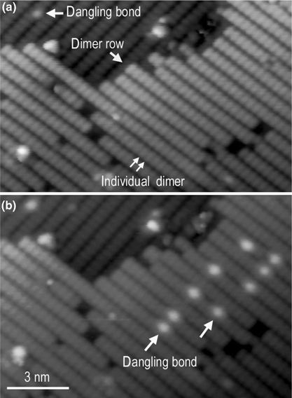
FIGURE 10.1 Selected area STM images of (a) as-prepared H-terminated Si(100)-(2×1) surface and (b) surface “a” after creation of few dangling bond sites by electron injection from STM tip. Scanning parameters: Vsample = –1.45 V (a) and –2.20 V (b); I = 0.2 nA. Electron pulse injection parameters: Vsample = –3.8 V; I = 0.5 nA, τ=0.5 s.
Ideally, a DB site contains an unpaired electron, which can act as a reactive radical site on the surface. When a molecule with suitable functionality is dosed on the surface, the DB site readily reacts with the molecule. It is observed that styrene and its derivatives such as methylstyrene, bromostyrene, or trifluoromethylstyrene undergo chain reaction with the DB site of the substrate and form a 1D nanostructure on the H-terminated Si(100)-(2×1) surface [15,17,19,21,22]. The typical STM images of such nanostructures formed through the reaction of styrene molecules with the dangling bond sites on the H-terminated surface are shown in Fig. 10.2 [15]. These sets of images reveal that the line-shaped nanostructure grown with increasing doses of styrene molecules is initiated at the DB sites indicated in Fig. 10.2a. The longest nanostructure in Fig. 10.2d is estimated to be ~130 Å long, corresponding to 34 dimers in a row. Sometimes growth of the nanostructures is observed to be stopped at a preexisting defect site. The 1D nanostructure formed by styrene derivatives such as methylstyrene, bromostyrene, and so on appears similar to that in Fig. 10.2 [19,21,22]. In addition to single 1D nanostructures, some doubled nanostructures, where both of the silicon dimer atoms are occupied, are also formed.
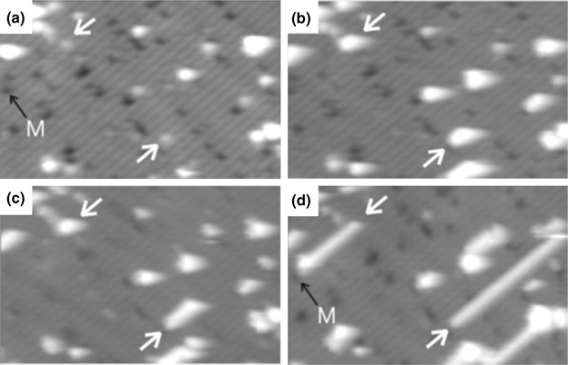
FIGURE 10.2 A sequence of STM images (25 nm × 14 nm, –2.1 V, 47 pA) corresponding to an increasing exposure to styrene: (a) 3 L; (b) 28 L; (c) 50 L; (d) 105 L. The white arrows denote two particular dangling bond sites that lead to the growth of long styrene nanostructures. The missing dimer defect (M) marked in the figure terminates the growth of the nanostructure in the top left-hand corner of the image. Reproduced from Ref. 15.
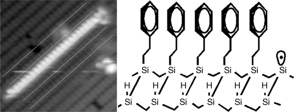
FIGURE 10.3 A high-resolution STM image of the nanostructure formed by styrene derivatives on the Si(100)-(2×1)–H surface revealing the individual adsorbed molecules. Reproduced from Ref. 21 by permission of the American Chemical Society. Vsample = –2.5 V; I = 0.2 nA. Scan area=8×8 nm2. Schematic of adsorbed styrene aligned one side of a dimer row is shown in the right panel.
A high-resolution STM image revealing the individual adsorbed molecules in a nanostructure is shown in Fig. 10.3. The 1D nanostructure is found to be located slightly off the center of the dimer row. The individual protrusions are spaced by 3.8 Å, corresponding to the distance between dimers in a row of the Si(100) surface. This image is consistent with molecules bound to adjacent dimers on the same side of a row, as shown in Fig. 10.3 (right panel). Note that the stacking of the phenyl rings in an assembly is important for determining the electronic properties of this 1D nanostructure. If the rings are parallel, some degree of overlap between π-states is expected, suggesting that the 1D nanostructure could function as a molecular wire [15]. The valence electronic states of such a 1D nanostructure are discussed in Section 10.3.3.
The reaction mechanism for the formation of a 1D nanostructure by styrene molecules is shown in Fig. 10.4 [15]. The initiation step of the chain reaction of styrene and other alkene molecules is the interaction of the >C=C< part with the DB of the substrate, which results in a C-centered intermediate radical, as shown in Fig. 10.4a and b (in the case of styrene). This intermediate radical (Fig. 10.4b) abstracts a H from the nearest dimer in a row resulting in a new DB site (Fig. 10.4c), which can react with another alkene molecule leading to a 1D nanostructure, as shown in Fig. 10.3.
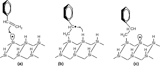
FIGURE 10.4 The chain reaction mechanism of styrene molecule with the dangling bond of the Si(100)-(2×1)–H surface.
Though the reaction steps involve only the C=C group and the DB bond site of the surface, all the molecules containing a C=C group do not undergo chain reaction forming the 1D nanostructure [28]. For example, allylbenzene, vinylcyclohexane, 4-vinylpyridene, propylene, and so on do not form nanostructures at room temperature [15,18,21,28]. It is suggested that the stabilization of intermediate radical to abstract H from the neighboring site plays an important role in promoting the chain reaction forming the nanostructure [18,32,33].
Reverse Chain Reaction
As seen in Figs. 10.3 and 10.4, the 1D nanostructure grown via the H abstraction mechanism should always be ended with a DB site unless the growth process encounters a defect site [15]. This end DB of a nanostructure can trigger a reverse chain reaction leading to the desorption of styrene molecule [15]. It is suggested that the observation of nanostructure on the surface by STM measurement depends on the relative rate of forward and reverse chain reaction at a given temperature. A controlled experiment with styrene molecules reveals that the reverse chain reaction at ~100°C is fast enough to completely desorb a whole nanostructure in a few minutes [24].
Figure 10.5 shows a series of STM images demonstrating the reverse chain reaction at elevated temperature. When the surface “a” was exposed to ~3 L of styrene at 300 K, four 1D nanostructures (i–iv) with different lengths (shown in Fig. 10.5b) were observed. The wider part of the line may be the doubled nanostructures. It was found that the length of the styrene line does not decrease even after several hours at 300 K. Since all of these growing 1D nanostructures (Fig. 10.5b) do not end at any preexisting defect, it is expected that there is a free DB at the end of each line, as shown in Fig. 10.3.
To see if the end DB of a nanostructure can initiate a reverse chain reaction to desorb styrene molecules, the temperature of the surface shown in Fig. 10.5b is gradually increased to 400 K while scanning of the same area is maintained. It is found that the length of the nanostructures does not decrease until the temperature of the surface reaches 400 K. Sequential measurements of STM images at 400 K (as shown in Fig. 10.5c–f) indicate that the length of a nanostructure gradually decreases to zero and leaves a DB at the same position (Fig. 10.5c–f and h) where it was originally located before the nanostructure growth (Fig. 10.5a). This suggests that desorption events occur through the chain reaction mechanism that is similar to, but the reverse of, the growth processes.
A schematic of the reaction mechanism for forward and reverse chain reactions of styrene molecules on the H-terminated Si(100)-(2×1) surface at 300 and 400 K, respectively, is shown in Fig. 10.6. In the reverse reaction, H from the adsorbed styrene goes back to the DB site (as indicated in Fig. 10.6c) followed by breaking of the Si–C bond (Fig. 10.6b). As mentioned earlier, the stabilization of the intermediate radical plays an important role in successful growth of a nanostructure. Computational studies have suggested that the stability of a C-centered radical and an adsorbed molecule adjacent to a DB is the key factor for the successful growth of nanostructures [18,32,33].
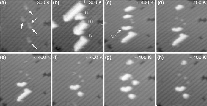
FIGURE 10.5 Series of STM images of the same area on the H-terminated Si(100)-(2×1) surface measured at 300 K (a, b) and 400 K (c, h). (a) Five dangling bonds indicated by arrows are created using high-voltage pulse injection from STM tip. The shadow feature of each DB is due to the tip artifact. (b) The surface “a” was exposed to ~3 L of styrene at 300 K. (c–f) Sequential STM images after the temperature of the surface “b” increased to 400 K. (g) The surface “f” was exposed to ~4 L of styrene at 400 K. (h) Three minutes after “g”. For (g), Vsample= –1.1 V; I=0.2 nA; scan area=9.2×6.3 nm2. For (h), Vsample =−1.8 V; I=0.2 nA; scan area=7.0×5.5 nm2. Reproduced from Ref. 24 by permission of the American Chemical Society.
From the direct observation of reverse chain reaction, one can estimate the activation barrier for desorption. The change in the number of molecules (N) in the “styrene” nanostructure as a function of time (t) is observed to be linear, as shown for the two different “styrene” nanostructures in Fig. 10.6d. The N versus t plots clearly suggest that desorption events of styrene molecules through the chain reaction mechanism are zero order; that is, the rate of reverse reaction is independent of the number of molecules in a nanostructure. The observed zero-order reaction is consistent with the fact that the molecule at the next nearest neighbor site to the DB plays no role in the desorption process of the molecule at the nearest neighbor site to the DB. The slight slope difference between the two lines (gray and black) is perhaps due to the difference in substrate temperature (±20 K).
Employing the zero-order rate equation (–dN/dt=k) in Fig. 10.6d, the average rate constant k for the reverse reaction at 400 K is estimated to be 1.17×10⁻² s–1. If the preexponential factor (v) is assumed to be 1014 s–1 (as in Ref. 15), Ed is estimated to be 1.26 ± 0.06 eV. This estimated activation barrier for the reverse reaction lies within the calculated values (0.90–1.43 eV) reported earlier [18,32,33]. Compared with that in the “styrene” nanostructure, the activation barrier for the reverse reaction in the 2,4-dimethylstyrene (2,4-DMS) nanostructure seems to be lower, as indicated by the frequent reverse reaction seen at 300 K. Neglecting the number of molecules adsorbed from the background, the rate constant k for 2,4-DMS at 300 K is estimated to be 2.59×10⁻²s–1, which gives an Ed value of 0.93 eV [24]. This lower Ed for 2,4-DMS compared to that for the “styrene” nanostructure may be related to the steric crowding of two methyl groups in the phenyl ring. These relative activation barriers for the desorption of styrene and methylstyrene are in agreement with the recent theoretical calculation [34].
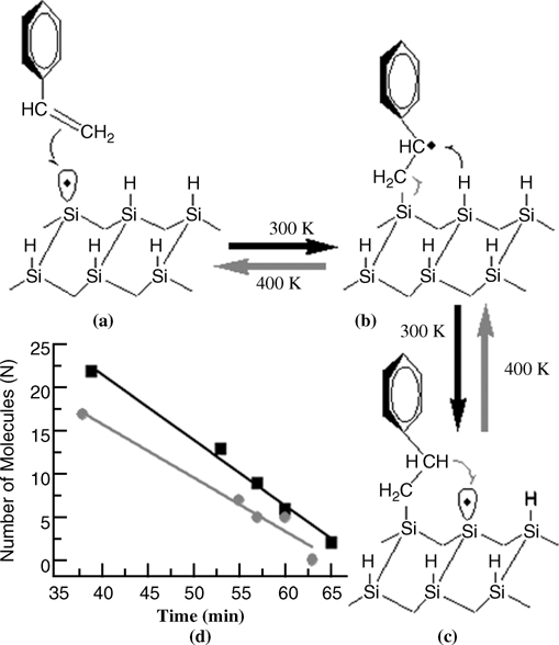
FIGURE 10.6 (a–c) Schematic of reaction mechanism for forward and reversed chain reactions of styrene molecules on H-terminated Si(100)-(2×1) surface at 300 and 400 K, respectively. (d) Change in number of molecules in two typical styrene nanostructures as a function of time at 400 K. The solid lines are the linear fit to the data points for two different styrene nanostructures. Reproduced from Ref. 24 by permission of the American Chemical Society.
10.3.1.2 Long-Chain Alkenes on Si(100)-(2×1)–H
A number of long-chain alkene molecules have been studied by DiLabio et al. [18]. They observed 1D nanostructure of only those alkene molecules whose chain length is higher than eight carbons (i.e., CnH2n; n ≥ 8) such as 1-octene, 1-undecene, 1-tertadecacene, and so on [18]. As discussed above, the desorption rate at a certain substrate temperature is crucial forobserving the 1D nanostructure in the STM image. If the desorption rate is so fast that all the molecules in a nanostructure desorb before the image is scanned, no 1D nanostructure will be seen in the STM image, even if the molecules might have undergone a chain reaction and formed a nanostructure during the exposure. Thus, the alkenes (i.e., CnH2n; n ≤ 8) that show no nanostructure growth at 300 K might show a nanostructure in the STM image at lower temperatures (<300 K) because of the reduced desorption rate. Indeed, 1-hexene and 1-heptene molecules are also found to undergo a chain reaction initiated at unpaired DB sites on the Si(100)-(2×1)–H surface, and to form a stable nanostructure at 180 K, as shown in Fig. 10.7 [24]. These observations widen the scope of nanostructure formation by various molecules.
10.3.1.3 Cross-Row Nanostructure
As discussed in previous sections, all the molecules such as styrene, styrene derivatives, alkenes, and so on form a 1D nanostructure only along the dimer row. However, to fabricate a nanostructure network on the surface, control over the directional selectivity of the nanostructure growth should be achieved. It is found that unlike other short-chain alkene molecules, allyl mercaptan readily undergoes chain reaction with the DB site and forms a 1D nanostructure even at room temperature [20]. In this particular case, the nanostructure is formed exclusively across the dimer row direction. Figure 10.8a shows the STM image of the Si(100)-(2×1)–H surface exposed to ~3 L of ALM molecules at 300 K. Four lines of small protrusions running across the dimer rows are 1D nanostructures formed by ALM molecules. These nanostructures are randomly distributed all over the surface, which suggests that the STM tip has no role in the growth of these nanostructures. All the observed nanostructures lie across the dimer rows. The high-resolution zoomed-in STM image (Fig. 10.8b) reveals that each protrusion in nanostructure has two parts, the “head” and “tail” as indicated in Fig. 10.8b. The “head” of a protrusion is located on the edge of a dimer row and its “tail” is on the preceding row (discussed later). The observed lines are stable even at 650 K (Fig. 10.8c) and for at least 10 days in vacuum at 300 K, which ensures that the molecules in the nanostructure are chemically bonded to the silicon substrate.
In accordance with the reported mechanism for the chain reaction of alkene molecules triggered at the DB site [14,15], the proposed mechanism for the Cross-row chain reaction by ALM molecules on Si(100)-(2×1)–H surface is shown in Fig. 10.9. Since propylene (CH2=CH–CH3) and allyl methyl sulfide (CH2=CH–CH2–S–CH3) do not show any nanostructure growth, the –SH group in ALM must have an important role in stabilization of the intermediate radical (Fig. 10.9b), which is the key for the successful growth of a nanostructure [15,18]. The chemistry of C-centered radical in the thiol molecule suggests that the radical centered at C can be transferred on S through tautomerism, and results in a thiyl radical (Fig. 10.9c), which is expected to be stable enough to abstract a H from the substrate.
The distance between the stable intermediate radical and the anchoring site of the molecule is one of the factors that determines the selectivity in the direction (across or along the dimer rows) of nanostructure growth. It is evident that the length of the ALM molecule makes it possible that the radical on the S atom (Fig. 10.9c) reaches to the nearest H on the next dimer row and abstracts it. To date, several computational studies have been reported regarding the detailed mechanism and energetics of the Cross-row chain reaction of allyl mercaptan [35–37]. Choi and Cho suggested that instead of H abstraction by thiyl radical, the sulfur atom makes a bond with the silicon atom followed by desorption of H2 from the dimer resulting in a DB site on the next silicon atom [36]. Thus, allyl mercaptan binds through the Si–C and Si–S bond across the dimer, thereby yielding a higher thermodynamic stability compared to other nanostructures (containing a single Si–C bond per molecule) grown along the dimer rows [36]. This success in forming a 1D nanostructure across the dimer rows provides a means to make a predesigned interconnection of nanostructures on the Si(100)-(2×1)–H surface.
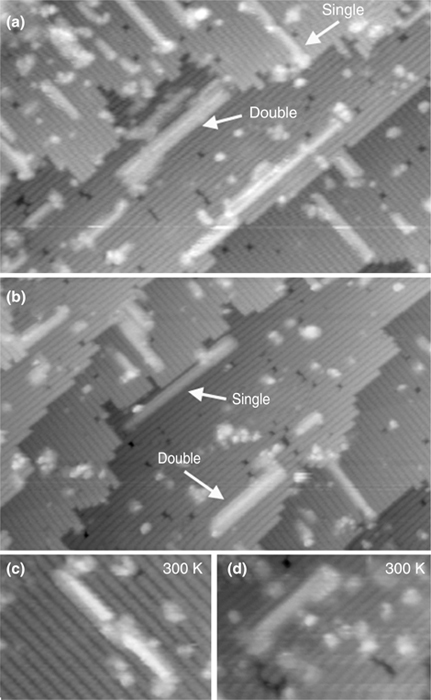
FIGURE 10.7 Selected area STM images of the Si(100)-(2×1)–H surface containing some nanostructures formed by DB-initiated chain reactions of (a) 1-hexene and (b) 1-heptene at 180 K. Typical single and doubled nanostructures are indicated. The doses of molecules for (a) and (b) are ~2 and ~8 L, respectively. (c) and (d) are STM images showing 1D nanostructure of adsorbed 1-hexene and 1-heptene after warming up the sample to 300 K. Vsample = – 2.5 V; I = 0.2 nA. Scan areas: (a) 48×30 nm2; (b) 54×34 nm2. Reproduced from Ref. 24 by permission of the American Chemical Society.
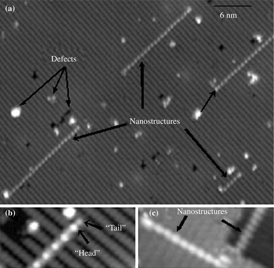
FIGURE 10.8 (a) STM image of Si(100)-(2×1)–H surface containing a dilute concentration of dangling bonds exposed to ~3 L of allyl mercaptan (CH2=CH–CH2–SH) molecules at 300 K. Vsample = –2.5 V; I=0.2 nA. (b) High-resolution zoomed-in image of nanostructure formed by allyl mercaptan at 300 K. Vsample = –1.2 V; I=0.2 nA. (c) STM image at 650 K. Vsample = –3.0 V; I = 0.2 nA. Reproduced from Ref. 20 by permission of the American Chemical Society.
10.3.1.4 Aldehyde and Ketone: Acetophenone–A Unique Example
In addition to the C=Cgroup, the >C=O group also reacts with the DB site leading to the formation of a nanostructure on the surface. Both aldehyde and ketone are observed to form nanostructures at room temperature. To date, a number of simple aldehydes and ketones such as acetaldehyde, bezaldehyde, cyclopropyl methyl ketone, acetone, acetophenone, and benzophenone molecules have been studied [23,28,38,39]. All these molecules except cyclopropyl methyl ketone undergo chain reaction with directional selectivity along the dimer row. Cyclopropyl methyl ketone shows poor directional selectivity resulting in random nanostructures on the surface [39]. It is found that acetone undergoes the most facile chain reaction among the molecules forming nanostructures along the dimer row on the surface.
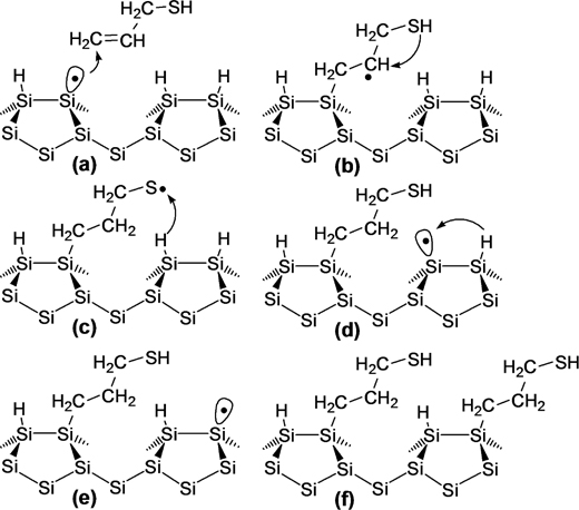
FIGURE 10.9 Proposed reaction mechanism for allyl mercaptan molecule with an unpaired dangling bond on H-terminated Si(100)-(2×1) surface.
A series of STM images demonstrating the formation of 1D nanostructures by dosing ~0.02 L of acetone molecules at 300 K are shown in Fig. 10.10. Acetone molecules always form a single nanostructure; that is, unlike styrene and other molecules that form nanostructures in the parallel-row direction [15,18,38], acetone molecules never form doubled nanostructures where both Si dimer atoms in a row are occupied by adsorbed molecules [23,28]. In rare events, only one or two underlying Si dimers are observed to be doubly occupied by acetone molecules in a 1D structure.
It was observed that the nanostructures formed by adsorbed acetone molecules are normally stable during scanning in the occupied state at sample biases below ~4.0 V. At higher scanning biases (>–5 V), the nanostructures were decomposed (data not shown). However, when a surface containing several freshly grown nanostructures was scanned in the unoccupied state, even at lower biases (e.g., at +2 V), some of the molecular lines disappeared leaving a clean H-terminated dimer row, as observed in Fig. 10.10c. This disappearance of nanostructure is also ascribed to the reverse chain reaction [24]. It seems that the scan at a positive sample bias (scanning in the unoccupied state) facilitates the reverse chain reaction in the present case.
The contrast of nanostructure of adsorbed acetone molecules in an STM image strongly depends on the bias voltage applied during scanning. As shown in Fig. 10.10d, the nanostructure appeared as depressions at a lower sample bias of –1.6 V, whereas they appeared as bright protrusions at –2.3 V (Fig. 10.10a–c). Careful inspection of Fig. 10.10d reveals that one-half of the dimer row appeared as depression (indicated by depressed half-row), while the other half appeared similarly to that of a clean H-terminated dimer row. In addition, the dimer row adjacent to the depression side appears wider (indicated in Fig. 10.10d) than that of a row in clean terrace. The depressed half-row in Fig. 10.10d lies on the same side of the dimer row at which the initial DB site is located in Fig. 10.10a (as shown in the inset). This registry of acetone line on a dimer row gives the direct observation of undergoing reaction paths of adsorbing molecules.
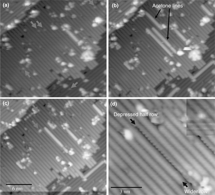
FIGURE 10.10 Selected area STM images of the Si(100)-(2×1)–H surface showing growth of nanostructures of adsorbed acetone molecules through chain reaction mechanism at 300 K. (a) Initial Si(100)-(2×1)–H surface containing several DB sites indicated by arrows. In addition to those DB sites, the surface also contains several defects and some preadsorbed molecules. (b) Surface “a” exposed to ~0.02 L of acetone molecules at room temperature. (c) Surface “b” after scanning at positive sample bias. Arrows indicate the dimer rows from which the nanostructure disappeared. (d) Selected area of surface “c” scanned at –1.6 V sample bias. The inset shows the location of a DB site in a dimer row. Vsample = –2.3 V (a–c); I = 0.2 nA (a–d). Reproduced from Ref. 23 by permission of the American Chemical Society.
Uniqueness of Acetophenone
Acetone and benzophenone form similar 1D nanostructures along the dimer row, and the adsorbed states of all molecules in a nanostructure are identical. In contrast, the 1D nanostructure of acetophenone molecules grows both “along” and “across” the dimer row, as shown in Fig. 10.11 [28]. The nanostructures lying across the dimer rows are indicated by a black arrow (Fig. 10.11a). The contrasts of nanostructures along and across the dimer rows are similar in the STM image; this establishes that both Cross-row and parallel-row nanostructures are formed by the same chemical species. The Cross-row nanostructures of adsorbed acetophenone molecules are clearly distinguishable from those of allyl mercaptan molecules; a Cross-row nanostructure formed by preexposure to a small amount (~0.02 L) of allyl mercaptan molecules is indicated by the gray arrow [20]. It is found that almost 30% of the 1D nanostructures formed by acetophenone molecules in Fig. 10.11a lie across the dimer rows. However, this percentage of Cross-row nanostructures varies depending on the cleanliness of the surfaces. Apparently, the higher concentration of dark defect sites (missing dimer and/or dihydride) on the surface favors the higher number of Cross-row nanostructures [20].
One can easily recognize that two different types of molecular arrangements exist in nanostructures along the dimer row (Fig. 10.11b). Some of the nanostructures resolved into many small protrusions, which are arranged in a zigzag pattern (indicated as “zigzag”), while others appear as uniform bar-like structure (indicated as “uniform”). These two different types of molecular arrangements can be seen together even within the same nanostructure; however, the boundary between the two arrangements cannot be clearly determined. It is found that almost 70% of nanostructures consist of zigzag arrangement of the small protrusions. In the case of nanostructures across the dimer rows, only the zigzag arrangements of small protrusions are observed, as shown in the lower right inset of Fig. 10.11b.
The CH3COCH3, PhCOPh, and PhCOCH3 contain only the >C=O reactive group, and the nanostructures are formed through a common chain reaction mechanism involving the >C=O group and DB site of the substrate, as shown in Fig. 10.12 [28,38]. Although the reactions leading to the formation of nanostructures by these molecules are basically similar, the directional selectivity of acetophenone molecules is different from that of acetone (CH3COCH3) and benzophenone (PhCOPh). Indeed, all the molecules that form well-defined nanostructures undergo chain reactions either along or across the dimer rows [28]. Hence, acetophenone is a unique example of an organic molecule that can lead to a DB-initiated chain reaction propagating both across and along the dimer rows on the Si(100)-(2×1)–H surface.
The unique behavior of the acetophenone is attributed to the formation of chiral carbon atom after adsorption (Fig. 10.12c), which did not happen for benzophenone and acetone molecules. Hence, depending on the spatial orientation of the CH3 and Ph groups, the chiral carbon atoms may attain the absolute configuration of R or S. Thus, the creation of a chiral center allows the acetophenone molecules to attain one of two possible stacking sequences (RSRS and RRR or SSS) along the growth direction as shown schematically in Fig. 10.13.
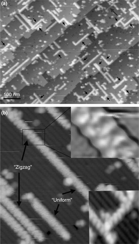
FIGURE 10.11 (a) STM images of the Si(100)-(2×1)–H surface exposed to ~10 L of acetophenone (PhCOCH3) molecules at 300 K. Before acetophenone exposure, the surface was preexposed to a small amount (~0.02L) of allyl mercaptan molecules. The black arrows indicate nanostructure grown across the dimer rows. The gray arrow indicates a Cross-row nanostructure formed by allyl mercaptan molecules. (b) A high-resolution STM image of a few nanostructures of adsorbed acetophenone. Two different appearances of the nanostructures are indicated as “zigzag” and “uniform.” Upper right inset: zoomed-in 3D view of a “zigzag” nanostructure. Lower right inset: high-resolution image of a Cross-row nanostructure. Nanostructures along the dimer row are also seen. Vsample = –2.1 V; I=0.2 nA. Reproduced from Ref. 28 by permission of the American Chemical Society.
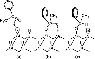
FIGURE 10.12 Schematic of the chain reaction mechanism of acetophenone and a DB site of the Si(100)-(2×1)–H surface along the dimer row.
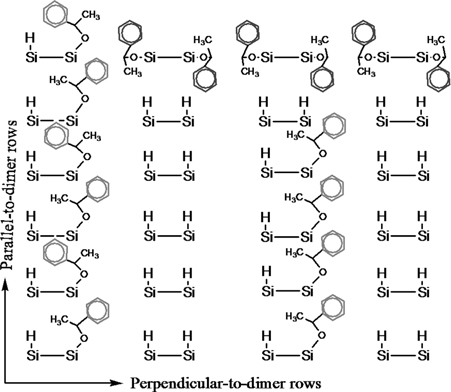
FIGURE 10.13 Schematic of the different types of molecular stacking of adsorbed acetophenone molecules along and across the dimer row direction on the Si(100)-(2×1)–H surface.
10.3.2 Interconnected Junctions of 1D Nanostructures
10.3.2.1 Perpendicular Junction
As discussed above, the growth of 1D nanostructure can be directed not only along but also across the dimer rows on Si(100)-(2×1)–H by selecting the appropriate molecular systems [21]. Thus, control over the growth direction allows to fabricate the interconnected nanostructure network on the surface. Figure 10.14a shows an STM image of the Si(100)-(2×1)–H surface exposed to ~5 L of ALM at 300 K. Two nanostructure of unequal lengths, running perpendicular to the dimer rows, are formed by adsorbed ALM molecules through the chain reaction mechanism [20].
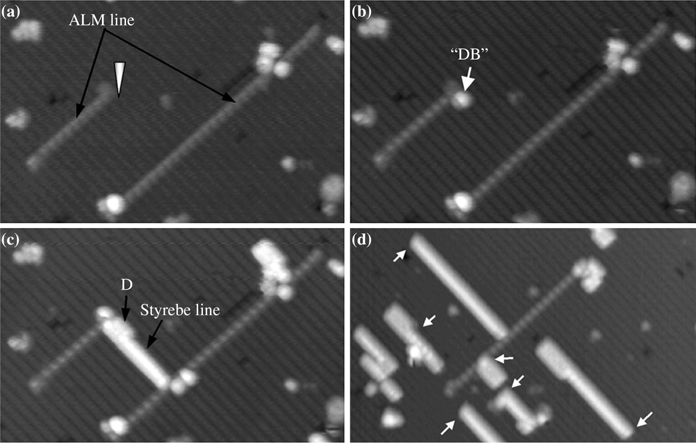
FIGURE 10.14 Selected area STM images of (a)the Si(100)-(2×1)–H surface containing two ALM nanostructures, (b) a dangling bond created using STM tip at the position shown in (a), and (c) the surface “b” exposed to ~5 L of styrene at room temperature. (d) The Si(100)-(2×1)–H surface containing an ALM nanostructure is exposed to 10 L of styrene after creating several DBs at the position indicated by arrows. Vsample = – 2.6 V; I=0.2 nA. Scan area: (a–c) 26×16 nm2; (d) 32×20 nm2. Reproduced from Ref. 21 by permission of the American Chemical Society.
Since there are several molecules that undergo the chain reaction along the dimer rows, it should be possible to connect those Cross-row nanostructures by a parallel-row nanostructure. To achieve this, a single DB is created at the position shown in Fig. 10.14a using high-voltage pulse injection from the STM tip. The bright protrusion indicated by “DB” in Fig. 10.14b may be the unpaired DB or a styrene molecule (from the background) already reacted with the freshly created DB. When the surface shown by Fig. 10.14b is exposed to ~5 L of styrene, a bright nanostructure connecting both the ALM nanostructures appeared (Fig. 10.14c). This newly appeared bright nanostructure is formed by styrene molecules.
In order to grow a styrene nanostructure that perpendicularly connects a preexisting ALM nanostructure, it is not essential to create DB adjacent to the ALM nanostructure as done in Fig. 10.14a. Since the styrene nanostructure can grow either side of the DB site along the dimer rows, a reaction initiated at a DB site located even a little away from the ALM nanostructure can eventually touch the ALM nanostructures. Figure 10.14d shows such growths of styrene nanostructures initiated by the DB sites located at different distances from an ALM nanostructure, in which arrows indicate the location of DB sites on the initial surface. It is observed that some of the styrene nanostructures have grown toward the ALM nanostructure and ultimately connected with it, while others have grown away from the ALM nanostructure.
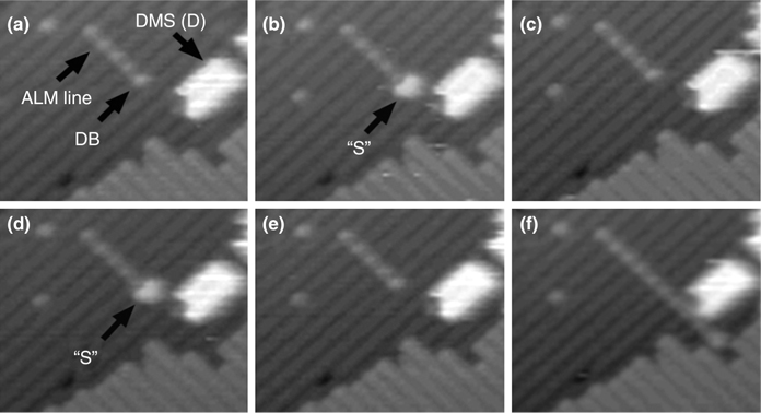
FIGURE 10.15 Selected area STM images of Si(100)-(2×1)–H surface showing (a) a growing ALM nanostructure with an end DB site and a nearby DMS doubled nanostructure, (b) the “a” exposed to 5 L of DMS, (c) 6 min after “b”, (d) the “c” exposed to 7 L of DMS, (e) 6 min after “d”, and (f) the “e” exposed to 0.5 L of ALM. Vsample = –2.5 V; I=0.2 nA. Scan area: (a–f) 11.2×9.6 nm2. Reproduced from Ref. 21 by permission of the American Chemical Society.
Note that there exists a DB site at the end of the molecular nanostructure (growing nanostructure) where the growth has not yet been terminated by a preexisting DB or defect, among others [15,21,24]. Hence, instead of creating a new DB at the vicinity of the ALM nanostructure, the end DB site of a growing nanostructure should also be able to initiate a nanostructure growth along the rows if the surface is exposed to styrene or DMS. However, the repeated attempts of growing a 1D nanostructure from the end DB of a growing ALM nanostructure were not successful, as demonstrated in Fig. 10.15. Though a single styrene molecule (denoted as “s”) is found to be adsorbed at the end DB site, no nanostructure is grown [21]. Instead, the adsorbed styrene at the end DB site desorbs in a few minutes as seen in Fig. 10.15c and e.
As noted above, acetone molecules undergo the most facile chain reaction with a DB site, which proceeds selectively on the Si(100)-(2×1)–H surface resulting in only a single 1D nanostructure along the dimer row. Indeed, the smaller size and higher reactivity of acetone molecules enable us to successively grow a parallel-row nanostructure from the end of a Cross-row nanostructure simply by changing the feed of gas molecules into the reaction chamber [23]. The interconnected junction of 1D nanostructures fabricated from a single DB site is shown in Fig. 10.16. The fabrication of such a 1D nanostructure from the end of a freshly grown ALM nanostructure, without creating any additional DB site, is well reproduced.
An attempt to grow an ALM nanostructure from the end of a nanostructure grown by acetone dosing was also made but did not succeed [21]. This limits the formation of a more extended junction of interconnected nanostructures on the surface. The low probability of ALM molecules to undergo a Cross-row chain reaction or the steric hindrance induced by the nearby adsorbed acetone molecule may be the reason for this.
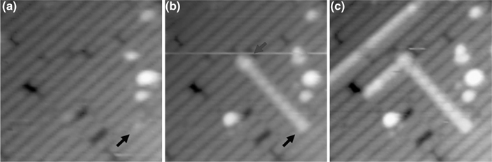
FIGURE 10.16 Successive growth of mutually perpendicular nanostructures by propagating a chain reaction from the Cross-row direction to the parallel-row direction on the Si(100)-(2×1)–H surface at 300 K. (a) Initial Si(100)-(2×1)–H surface containing a DB site indicated by black arrow. (b) Surface “a” exposed to ~0.4 L of ALM molecules. The black and gray arrows indicate the initiation and end of ALM nanostructure growth, respectively. (c) Surface “b” exposed to ~0.2 L of acetone molecules. Scan area=11×11 nm2. Vsample = –2.6 V; I=0.2 nA. Reproduced from Ref. 23 by permission of the American Chemical Society.
10.3.2.2 One-Dimensional Heterojunction
In addition to growing of L-shaped junction of 1D nanostructure, a nanostructure consisting of different molecules can also be fabricated by alternate dosing of different molecules that undergo chain reaction in the same direction. The growth of 1D heteromolecular junctions consisting of styrene/CH3-styrene and CF3-styrene/CH3O–styrene systems has been reported [19,31]. Very recently, Walsh et al. [30] have demonstrated such heterostructure consisting of styrene and phenylacetylene (PA). Unlike styrene nanostructures, no doubled nanostructures are observed for PA. However, Fig. 10.17 reveals an instance of a heteromolecular doubled 1D nanostructure. In this case, one side of the doubled nanostructure (the left side) is composed entirely of styrene, while the other side (the right side) consists of a block of styrene and a block of PA. Since only one binding site is available per silicon dimer for PA in the heteromolecular doubled nanostructure, each PA molecule must be bound to the surface via only one silicon atom in this case. It should be noted that the STM image of the PA portion of the doubled chain nanostructure appears identical to the other isolated PA nanostructures. Consequently, it can be concluded that the PA molecules in single 1D nanostructures are also bound to only one silicon atom on the surface, as shown in Fig. 10.17 (right panel) [30].
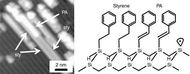
FIGURE 10.17 STM image showing the styrene–phenylacetylene heterostructures (left panel), and schematic model for a heterostructure (right panel) on Si(100)-(2×1)–H surface. Reproduced from Ref. 30 by permission of the American Chemical Society.
10.3.3 UPS of 1D Nanostructures on the Surface
The prospect of utilization of 1D nanostructure as a basic component of a molecular device essentially depends on the extent of interaction between the π-orbital and substrate electronic states, the π–π interaction between neighboring molecules in a nanostructure, and the effects of substituents on these interactions [40–42]. To understand these phenomena, it is essential to explore the valence states of such 1D nanostructures on the surface.
Valence electronic states of benzophenone, acetophenone, and acetone have been studied using UPS at room temperature [29]. Figure 10.18a(iii) shows the UPS spectrum of 1D structures of adsorbed benzophenone on the Si(100)-(2×1)–H surface at room temperature. The spectra of bare and H-terminated Si(100)-(2×1) are included as Fig. 10.18a(i) and (ii). The typical STM images of the surfaces corresponding to the spectra (ii) and (iii) are shown as Fig. 18b and c, respectively. All spectra are recorded with photon energy of 21.2 eV. The bare Si (100)-(2×1) surface is characterized by the surface state (SS) peak at ~0.8 eV below the Fermi level, as observed in the spectrum (i) [43]. For the H-terminated Si(100)-(2×1) surface (Fig. 10.18a(ii)), the peak at 0.8 eV disappeared and some weak features at higher binding energies (~1.9, 3.5, 5.6, and 7.6 eV) are observed, which is in agreement with the previous reports [44]. No peaks related to the DB sites appeared in the UPS spectrum because of very low concentration (roughly estimated to be ~0.4% of the surface silicon atoms) of the DB sites on the surface.
Although the concentration of the adsorbed molecules was estimated to be only ~6%, the UPS spectrum of these 1D nanostructures on H-terminated Si(100)-(2×1)–H surface clearly shows the intense peaks at 3.8, 6.8, 9.0, and 11.2 eV below the Fermi level [29]. Comparison of the UPS spectrum of benzophenone nanostructures on the surface (Fig. 10.18a(iii)) with that of the H-terminated surface (Fig. 10.18a(ii)) clearly indicates that these peaks arise from the nanostructure of the adsorbed benzophenone.
The UPS spectra of 1D nanostructures formed by acetophenone and acetone molecules help to explore the origin of the peaks observed for benzophenone nanostructures [29]. The comparison of the UPS spectra of acetone nanostructures with that of benzophenone (or acetophenone) nanostructures clearly indicates that the major peaks at 3.8, 6.8, 9.0, and 11.2 eV in the benzophenone spectrum arise due to the presence of the phenyl rings of the adsorbed molecules. The relative positions of these peaks with respect to the higher binding energy (11.2 eV) peak seem very similar to that of solid benzophenone; that is, the energy of molecular orbitals related to phenyl rings does not change significantly after the adsorption of molecules on the Si(100)-(2×1)–H surface (Fig. 10.19). This suggests that the phenyl rings of the adsorbed molecule have little or no interaction with the surface silicon atoms. According to the assignments of the peaks observed for solid benzophenone and multilayer benzene on the silicon surface [44,45], the peaks are qualitatively ascribed as 3.8 eV to Phπ, 6.8 eV to Phπ+σ, 9.0 eV to Phσ, and 11.2 eV to Phσ orbitals [45].
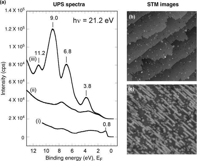
FIGURE 10.18 (a) UPS spectra of (i) bare Si(100)-(2×1), (ii) H-terminated Si(100)-(2×1), and (iii) one-dimensional nanostructures of adsorbed benzophenone on the Si(100)-(2×1)–H surface. For clarity, the base line of the spectra (ii) and (iii) was shifted upward by the same scale. The typical STM images of the surfaces corresponding to (ii) and (iii) are shown as (b) and (c), respectively. Vsample = – 2.4 V (a) and -2.7 V (b). Itunnel=0.2 nA. Scan area=80×80 nm2. Reproduced from Ref. 29 by permission of the American Chemical Society.
Although the UPS measurement does not give any direct evidence, one can predict a weak π–π interaction among the molecules of a nanostructure similar to (or a little higher than) the one that exists in benzophenone crystal. The relatively larger width of the lowest energy peaks and the absence of fine structure in Fig. 10.19a(iv) may relate to a higher π–π interaction between molecules in a nanostructure compared to the one that exists in benzophenone crystal. Indeed, a weak π–π interaction among the molecules separated by 3.8 Å has also been predicted by DFT calculation, where the dispersion of the π-band along the molecular assemblies was estimated to be ~0.4 eV [40].
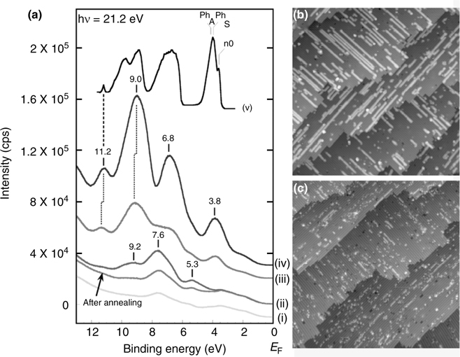
FIGURE 10.19 (a) UPS spectra of one-dimensional nanostructures of (i) H-terminated Si(100)-(2×1), (ii) adsorbed acetone (before and after annealing), (iii) acetophenone and (iv) benzophenone on the Si(100)-(2×1)–H surface at 300 K. The photoelectron spectrum of (v) solid benzophenone is also included for comparison. The spectrum of solid benzophenone was reproduced from Ref. 45 and aligned with the higher binding energy peak of benzophenone by the energy shift of ~1 eV. For clarity, the base line of the spectra was shifted. (b) and (c) show the STM images of the nanostructures of adsorbed acetone on the Si(100)-(2×1)–H surface and the same surface annealed to 600 K, respectively. Scan area = 80×80 nm2. Vsample = –2.5 V; I = 0.2 nA. Reproduced from Ref. 29 by permission of the American Chemical Society.
10.4 CONCLUSIONS
Formation of organic nanostructures on semiconductor surfaces has particular interest from the perspective of molecular electronics. Unpaired dangling bond-initiated chain reaction has appeared as the most prominent and precise method for controlled fabrication of 1D organic nanostructure networks on the Si(100)-(2×1)–H surface. A variety of molecules with >C=C<, >C=O, –HC=O, and –C=C– groups undergo DB-initiated chain reaction on the Si(100)-(2×1)–H surface and form 1D nanostructures on the surface. The successful growth of nanostructures is limited by the relative rate of forward and reverse chain reaction. The position, length, and composition, as well as the alignment of these nanostructures, are precisely controllable. Formation of different types of nanostructures, such as straight homogeneous, perpendicularly connected, and linearly connected heterogeneous nanostructures, has been demonstrated. The valence electronic states measurement suggests that the electronic states of phenyl π-orbitals stacked parallel to each other remain largely decoupled from the substrate electronic states, and the π–π interaction within the nanostructures formed by benzophenone is relatively weak. These studies regarding the controlled fabrication of 1D organic nanostructure networks on the H-terminated Si(100) surface are expected to have substantial impact on promoting further studies focusing on the functional nanoscale device.
ACKNOWLEDGMENT
This work is supported in part by the Grant-in-Aid for Scientific Research on Priority Areas “Electron transport through a linked molecule in nano-scale” (No. 17069006) from the Ministry of Education, Culture, Sports, Science and Technology (MEXT), Japan and the Program to Disseminate Tenure-Track System of the MEXT granted to Gunma University.
REFERENCES
1. Aviram, A.; Ratner, M. A. Chem. Phys. Lett. 1974, 29, 277.
2. Joachim, C.; Gimzewski, J. K.; Aviram, A. Nature 2000, 408, 541.
3. Nitzan, A.; Ratner, M. A. Nature 2003, 300, 1384.
4. (a) Ratner, M. Nature 2005, 435, 575. (b) Guisinger, N. P.; Yoder, N. L.; Hersam, M. C. Proc. Natl. Acad. Sci. USA 2005, 102, 8838.
5. Piva, P. G.; DiLabio, G. A.; Pitters, J. L.; Zikovsky, J.; Rezeq, M.; Dogel, S.; Hofer, W. A.; Wolkow, R. A. Nature 2005, 435, 658.
6. Eigler, D. M.; Schweizer, E. K. Nature 1990, 344, 524.
7. Stroscio, J. A.; Eigler, D. M. Science 1991, 254, 1319.
8. Lehn, J.-M. Angew. Chem., Int. Ed. Engl. 1988, 27, 89.
9. Lehn, J.-M. Angew. Chem., Int. Ed. Engl. 1990, 29, 1304.
10. Wolkow, R. A. Annu. Rev. Phys. Chem. 1999, 50, 413.
11. (a) Bent, S. F. Surf. Sci. 2002, 500, 879. (b) Hamers, R. J. Nature 2001, 412, 489.
12. Shen, T. C.; Wang, C.; Abeln, G. C.; Tucker, J. R.; Lyding, J. W.; Avouris, Ph.; Walkup, R. E. Science 1995, 268, 1590.
13. Boland, J. J. J. Vac. Sci. Technol. A 1992, 10, 2458.
14. Linford, M. R.; Fenter, P.; Eisenberger, P. M.; Chidsey, C. E. D. J. Am. Chem. Soc. 1995, 117, 3145.
15. Lopinski, G. P.; Wayner, D. D. M.; Wolkow, R. A. Nature 2000, 406, 48.
16. Kruse, P.; Johnson, E. R.; DiLabio, G. A.; Wolkow, R. A. Nano Lett. 2002, 2, 807.
17. Basu, R.; Guisinger, N. P.; Greene, M. E.; Hersam, M. C. Appl. Phys. Lett. 2004, 85, 2619.
18. DiLabio, G. A.; Piva, P. G.; Kruse, P.; Wolkow, R. A. J. Am. Chem. Soc. 2004,126, 16048.
19. Kirczenow, G.; Piva, P. G.; Wolkow, R. A. Phys. Rev. B 2005, 72, 245306.
20. Hossain, M. Z.; Kato, H. S.; Kawai, M. J. Am. Chem. Soc. 2005, 127, 15030.
21. Hossain, M. Z.; Kato, H. S.; Kawai, M. J. Phys. Chem. B 2005, 109, 23129.
22. Basu, R.; Kinser, C. R.; Tovar, J. D.; Hersam, M. C. Chem. Phys. 2006, 326, 144.
23. Hossain, M. Z.; Kato, H. S.; Kawai, M. J. Am. Chem. Soc. 2007, 129, 12304.
24. Hossain, M. Z.; Kato, H. S.; Kawai, M. J. Am. Chem. Soc. 2007, 129, 3328.
25. Zikovsky, J.; Dogel, S. A.; Haider, A. B.; DiLabio, G. A.; Wolkow, R. A. J. Phys. Chem. A 2007, 111, 12257.
26. Dogel, S. A.; DiLabio, G. A.; Zikovsky, J.; Pitters, J. L.; Wolkow R. A. J. Phys. Chem. C 2007, 111, 11965.
27. Wang, Q. H.; Hersam, M. C. J. Am. Chem. Soc. 2008, 130, 12896.
28. Hossain, M. Z.; Kato, H. S.; Kawai, M. J. Am. Chem. Soc. 2008, 130, 11518.
29. Hossain, M. Z.; Kato, H. S.; Kawai, M. J. Phys. Chem. C 2009, 113, 10751.
30. Walsh, M. A.; Walter, S. R.; Bevan, K. H.; Geiger F. M.; Hersam, M. C. J. Am. Chem. Soc. 2010, 132, 3013.
31. Piva, P. G.; Wolkow, R. A.; Kirczenow, G. Phys. Rev. Lett. 2008, 101, 106801.
32. Cho, H. J.; Oh, H. D.; Kleinman, L. Phys. Rev. B 2002, 65, 081310.
33. Kang, J. K.; Musgrave, C. B. J. Chem. Phys. 2002, 116, 9907.
34. Takeuchi, N.; Kanai, Y.; Selloni, A. J. Phys. Chem. C 2010, 114, 3981.
35. Ferguson, G. A.; Than, C. T. L.; Raghavachari, K. J. Phys. Chem. C 2009, 113, 18817.
36. Choi, J. H.; Cho, J. H. Phys. Rev. Lett. 2009, 102, 166102.
37. Ferguson, G. A.; Than, C. T. L.; Raghavachari, K. J. Phys. Chem. Lett. 2010, 1, 679.
38. Pitters, J. L.; Dogel, I.; DiLabio, G. A.; Wolkow, R. A. J. Phys. Chem. B 2006, 110, 2159.
39. Tong, X.; DiLabio G. A.; Clarkin, O. J.; Wolkow, R. A. Nano Lett. 2004, 4, 357.
40. (a) Rochefort, A.; Boyer, P. Appl. Phys. Lett. 2006, 89, 092115. (b) Rochefort, A.; Boyer, P.; Nacer B. Org. Electron. 2007, 8, 1.
41. Rochefort, A.; Martel, R.; Avouris, Ph. Nano Lett. 2002, 2, 877.
42. Geng, W. T.; Oda, M.; Nara, J.; Kondo, H.; Ohno, T. J. Phys. Chem. B 2008, 112, 2795.
43. Gokhale, S.; Trichberger, P.; Menzel, D.; Widdra, W.; Dröge, H.; Steinrück, H.-P.; Birkenheuer, U.; Gutdeutsch, U.; Rösch, N. J. Chem. Phys. 1998, 108, 5554.
44. Ciraci, S.; Butz, R.; Oellig, E. M.; Wager, H. Phys. Rev. B 1984, 30, 711.
45. McAlduff, E. J.; Bunbury, D. L. J. Electron Spectrosc. Relat. Phenom. 1979, 17, 81.
Functionalization of Semiconductor Surfaces, First Edition
Edited by Franklin (Feng) Tao and Steven L. Bernasek.
© 2012 John Wiley & Sons, Inc. Published 2012 by John Wiley & Sons, Inc.