
CHAPTER 12
Chemical Stability of Organic Monolayers Formed in Solution
LESLIE E. O'LEARY, ERIK JOHANSSON, AND NATHAN S. LEWIS
12.1 REACTIVITY OF H-TERMINATED SILICON SURFACES
12.1.1 Background
The H–Si surface is important to the electronics and photovoltaics industries because Si–H is the starting point for many Si-based devices. In turn, the electronic and chemical properties of the H-terminated Si surface affect the properties of subsequent Si surfaces and interfaces [1–3]. Dangling or weak bonds present at the surface will affect minority-carrier (“excited-state”) processes, and will thus affect devices such as field-effect transistors and photovoltaics. Furthermore, the topography of, as well as the presence of adsorbed chemical contaminants on, a H-terminated Si surface greatly affects the electronic properties of Si/SiOx interfaces formed from this initial H-terminated Si surface [4,5]. Organic contaminants are difficult to remove from the Si surface, and different cleaning procedures have been shown to result in a variety of contaminant fingerprints. Hence, significant effort has been directed to understand the reactivity of the H–Si surface.
This section will explore the reactivity of the H-terminated Si surface with O2, H2O, alcohols, metals, amines, and thiols. The synthesis, as well as the physical and electronic characterization, of the H–Si surfaces will be reviewed briefly, but the reader is encouraged to consult Chapter 3 for a more detailed account of the preparation and characterization of H-terminated Si surfaces.
12.1.1.1 Synthesis of H-Terminated Si Surfaces
The H-terminated Si surface can be formed by a variety of procedures, including vacuum techniques, electrochemical etching, and chemical etching [6–14]. H-terminated surfaces prepared by vacuum cleavage of Si, followed by exposure to hydrogen, have been studied using high-resolution electron energy loss spectroscopy (HREELS) and other ultrahigh vacuum techniques [10,11]. Low-energy electron diffraction (LEED) studies have indicated that the surface order does not change upon exposure of a freshly cleaved surface to hydrogen.
Although such techniques enable investigation of the properties of very pure H-terminated surfaces, vacuum cleavage of bulk crystals is not suitable for large-scale processing. A significant amount of effort has thus been devoted to elucidating the behavior of solution-based routes to H-terminated Si surfaces. The composition of the Si surface following HF etching has been studied using multiple internal reflection Fourier transform infrared (MIR-FTIR) spectroscopy. The presence of IR absorption bands ascribable to Si–H, Si–H2, and Si–H3 moieties indicated that aqueous HF etching of Si(111) yielded microscopically rough surfaces, but linewidth analysis suggested that the surfaces were locally ordered [12–14].
The ability to create atomically flat Si(111) surfaces using a wet chemical approach (Fig. 12.1) was discovered in 1989. The method built on the observation that HF etching of Si(111) and Si(100) induced microscopic roughness to the surfaces [12,15]. Following these studies, the effects of pH were examined to elucidate the effects of the HF(aq) concentration on Si surface quality [15,16]. Etching in buffered HF, in which the pH was adjusted using either NH4OH(aq) or HCl(aq), produced very different results than when the Si was etched in HF(aq) alone. Specifically, when the pH was greater than 4, a dramatic change occurred in the Si–H region of the FTIR spectra. A single, dominant peak, attributable to the Si–H stretching vibration, was produced with no peaks ascribable to the di-and trihydride species that were observed on surfaces etched in acidic HF(aq) solutions.
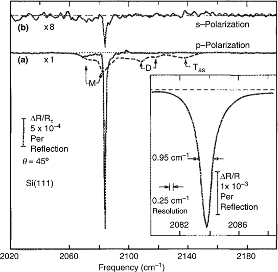
FIGURE 12.1 Internal reflection IR spectra of fluoride-etched Si(111) surfaces etched in acidic, dilute HF solution (100:1 H2O:HF) (dashed curve) and buffered HF (pH 9–10) (solid curve) probed under p-polarized light (a) and s-polarized light (b) [16]. Inset shows high-resolution spectrum of Si(111) etched in buffered HF. Reproduced from Ref. 16 by permission of the American Institute of Physics, © 1990.
In alkaline solution, the rate-determining step of the fluoride etch on Si is OH− attack. Simulations have shown that the relative reaction rates of OH− attack on features commonly encountered on a Si(111) surface, including kinks, dihydride, and monohydride steps, can differ by as much as eight orders of magnitude. The anisotropy of the basic fluoride etch is significantly decreased by the introduction of trace metal, oxygen, or other impurities into the etching solution [17,18]. Introduction of O2 into an NH4F(aq) etching solution greatly reduces the fidelity of the resulting Si(111) surface, producing Si–H2 and Si–H3 surface sites, as well as adding to the incorporation of O atoms into the Si–Si back-bonds. Scanning tunneling microscopy (STM) images clearly show the effect of the presence of oxygen in the NH4F(aq) etching solution. Without oxygen, the surface is dominated by large terraces of Si(111), whereas rough surfaces are produced by O2-containing NH4F(aq) etching solutions [17,18].
To further investigate the quality of the Si(111) surface, vacuum STM images and LEED patterns were obtained [15]. LEED patterns suggested that both HF(aq) and NH4F(aq) etching resulted in high-quality (1×1) surfaces with defect densities of 0.5%. Vacuum STM data, however, showed clear differences in the surface morphology produced by HF(aq) versus NH4F(aq) etchants, consistent with the presence of Si monohydride, dihydride, and trihydride peaks for HF(aq)-etched Si(111) surfaces, and consistent with only a sharp Si–H stretch in the IR spectrum of the NH4F(aq)-etched surfaces. For NH4F(aq)-etched surfaces, flat terraces extending thousands of Ångströms were observed with less than 1% surface contamination. The level of surface contamination seemed to not be intrinsic to the NH4F(aq) etching procedure. X-ray photoelectron (XP) spectra further confirmed that neither oxygen nor carbon constitute significant contaminants on surfaces prepared through the NH4F(aq) etch [17,19].
The techniques commonly used to characterize Si interfaces electronically were developed to study the Si/SiO2 or Si/metal interface [22]. The formation of Si/SiO2 structures and Si/metal junctions, however, rarely preserves the H-terminated Si surface. Consequently, almost all techniques used to study the H–Si surface are contactless [2,23], or form only soft contacts [24–26]. Using a contactless device, the H-terminated Si has been shown to be very well passivated electronically. Measurements taken in HF(aq) or in other strong acids yielded minority-carrier lifetimes >10 ms, suggesting that defect densities were as low as 1 per 40 million surface atoms [2]. The possibility that measurements in various solvents yielded long minority-carrier lifetimes due to band bending was investigated extensively, and it was found that one must proceed cautiously when correlating minority-carrier lifetimes to surface defect densities [27–30]. The highly ideal, flat, H-terminated Si(111) surface is attractive from an experimental point of view as it is a very well-defined system.
12.1.2 Reactivity of H–Si
The chemistry of the initial, H-terminated, Si surface greatly affects the properties of subsequent surfaces and interfaces [1–3]. The reactivity of unreconstructed Si(111) and Si(100) H-terminated Si surfaces has been thoroughly investigated. The (100) surface is of interest because the interatomic spacing of the Si atoms is well matched to the lattice constant of SiO2. This behavior has led to Si(100) being the predominant orientation of Si wafers used in the electronics industry [31]. However, the (111) surface is an attractive model system for scientific investigation because of the ability of the NH4F(aq) etch to form well-defined, high-quality H–Si(111) surfaces. In the following sections, the reactivity of H-terminated Si surfaces will be discussed, with emphasis on systems in which the reactivity affects the electronic properties of the resulting surfaces.
12.1.2.1 Aqueous Acidic Media
The reactivity of H–Si with aqueous acidic media has been extensively evaluated [32–35]. Perhaps one of the most well-known examples of H–Si reacting with an aqueous acidic solution is the “SC-2 clean,” in which H–Si is reacted with a H2O:H2O2: HCl mixture to ultimately yield a Si surface that is free of organic or inorganic contaminants. The chemistry of H–Si in aqueous acidic media is highly dependent on both the acid and the presence of any additional reactants or reagents. Depending on the solution composition, H–Si surfaces are protected in some acidic media, oxidize in other media, and dissolve in yet others. In contrast to alkaline HF etching described above, reactivity of Si in acidic media is highly isotropic.
In the absence of fluoride ions or oxidizing reagents, H–Si is stable in concentrated acids. This behavior is expected, because the high [H+] keeps the surface fully H-terminated. H–Si surfaces immersed in strong acids exhibit excellent electronic properties [2]. The lifetime of photogenerated minority carriers was measured using a contactless method, wherein the carrier density was measured using an inductively coupled RF bridge. The surface recombination velocity (SRV), which is related to the electronic defect density on the surface, was very low for such surfaces. Low SRV values were observed in a number of strong acids, and the SRV was a function of acid molarity. Furthermore, changing the acid molarity induced reversible changes to the surface recombination velocity. From the dependence on [H+], it was suggested that H–Si surfaces contain a finite number of strained, or otherwise weak, bonds, that act as recombination centers. The recombination centers resembled Lewis bases in an acid-base equilibrium with the surrounding solution, and the observed effect of acid molarity on SRV was ascribed to neutralization (H termination) of these defect sites [2].
In contact with an acidic aqueous solution that contains oxidants, the near-surface layer of such H-terminated Si(111) surfaces is rapidly converted to 1–2 nm of SiOx [34]. The SiOx passivates the surfaces to further oxidation, because HF-free solutions that contain oxidizers do not etch SiOx. As part of the Si cleaning procedure developed at RCA laboratories, oxidation of H–Si in HCl(aq)/H2O2(aq) has been widely utilized [35,36]. The RCA cleaning procedure removes a variety of organic contaminants and leaves low levels of metal contaminants.
The incorporation of fluoride ions into acidic media causes etching of Si and SiOx. SiOx etches very quickly in HF(aq); however, H–Si surfaces are more stable, etching at rates <1 Å/min. The etch rate increases dramatically when oxidizers are added to the HF(aq) solution [35], and numerous systems composed of H2O, HF, and an oxidizer have been employed to rapidly etch Si [37]. Specifically, the HF(aq)/ HNO3(aq) system etch rate is mm/min [36].
12.1.2.2 Aqueous Basic Media
The H-terminated Si surface is unstable in alkaline media. The etching of Si in alkaline media has been studied extensively [32]. The alkaline etching of Si is anisotropic and thus it proceeds very differently from etching in acidic, fluoride-containing, media [33]. The etch rates of single-crystal Si have been investigated as a function of crystallographic orientation (Table 12.1) [38]. The use of a large hemispherical Si crystal allowed for monitoring of the etch rates at higher index planes. The orientation-dependent etch rates were functions of [OH−] and temperature. The alkaline etching of Si also depends on both [H2O] and [OH−]. In organic alkaline solutions, the etch rate goes to zero as [H2O] approaches zero. In all cases, the etch rate of the (111)-oriented crystal face was considerably lower than the etch rates of the other faces. A reaction scheme for the dissolution of (100) oriented Si is presented in Fig. 12.2.
The replacement of H atoms with -OH− groups polarizes the Si back-bonds such that H2O can attack. The rate-limiting step determined whether a surface was left either H-terminated or OH-terminated. The mechanism of Fig. 12.2 explains why the alkaline etches are anisotropic, because the (111) surface is much more stable with only one bond left to be OH-terminated, while three are involved in back-bonding. With only one -OH group, the back-bonds are less activated, and H2O is less likely to attack and break the back-bonds.
TABLE 12.1 Orientation-Dependent Etch Rates (Relative to (110)) in mm/min as a Function of [KOH] at 70° C [38]
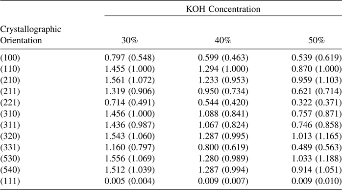
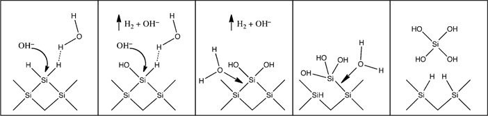
FIGURE 12.2 Proposed reaction scheme for the chemical dissolution of Si in basic media. Redrawn from Ref. 32.
In alkaline aqueous solutions that contain an oxidizing agent, hydrogen-terminated Si surfaces rapidly convert to Si covered with a thin overlayer of SiOx. The conversion of H–Si to SiOx has been studied extensively for RCA-1, NH4OH/H2O/H2O2 [35–37]. The amount of oxidizer present in the alkaline aqueous solution determines whether a SiOx overlayer will form and thus protect the Si from further alkaline etching. If only small amounts of oxidizer are present, the surface will be continuously etched by the hydroxide ions.
12.1.2.3 Oxygen-Containing Environments
Electronics must be robust in air, so the stability of HF-etched Si surfaces in oxygen-containing environments has been investigated quite thoroughly. The mechanism of the initial oxidation of H–Si surfaces is not fully understood, but many important aspects have been observed and described. The growth rate of SiOx on Si(100) was measured to be 0.2 nm/decade (hours), with a limiting oxide thickness of <1.4 nm as determined using XPS [39]. Conflicting results exist as to the effect of microscopic roughness on the rates of initial oxidation, but recent data suggest that the oxidation rates depend on the surface roughness [40,41].
Oxidation of H-terminated Si in the presence of O2 has also been investigated for the special case of oxidation in a pure oxygen, low-pressure (1–15 mTorr) environment at elevated temperatures (530–590 K). The reaction rate constants between O2 and various Si surface moieties, such as monohydrides and dihydrides present on various crystal phases, differed by as much as 20-fold. The monohydride-terminated surfaces were substantially more stable than the other surfaces. Si(111) surfaces oxidized significantly more slowly than Si(100) surfaces, and dihydride steps on Si (111) surfaces oxidized more rapidly than monohydride steps. Flat Si(111) surfaces were the most stable. It was suggested that neither O2 nor H2O alone could explain the rapid rates of native oxide formation commonly observed, and perhaps radicals or other trace contaminants are responsible for the observed rate of oxide formation [41]. Curiously, the initial oxidation of H–Si surfaces proceeds without loss of atop Si–H bonds. Oxygen inserts into the Si back-bonds without the formation of Si–OH species [41,42].
12.1.2.4 Alcohols
Alcohols are commonly used solvents for chemical reactions and cleaning procedures; thus, their interaction with H-terminated Si is of great interest. The H– Si surface is stable in a number of solvents including acetonitrile [43], toluene and mesitylene [43], and diethyl ether [44]; however, H–Si surfaces react with various alcohols [28,43,45,46]. Early investigations of reactions between H– Si and alcohols utilized porous Si, which provided for improved signal to noise in spectroscopic studies and allowed further investigation through the luminescence properties of porous Si. Methanol was attached to porous Si through electrochemical processes involving partial dissolution of the Si substrate [47], though simply exposing the H–Si to methanol has been seen to be sufficient for CH3O– attachment. Various studies have reported that attachment of alcohols to H–Si proceeds with partial oxidation of the underlying substrate [48,49], while others have successfully formed Si–O–C bonds without oxidation of the substrate [50,51]. The reactivity between alcohols and H–Si was used to form ferrocene-modified Si electrodes. The ferrocene was covalently linked to H–Si(111) simply by immersion in a ferrocene derivative that contained a terminal –OH group. Immersion in other alcohols also yielded modified surfaces, although the bonding and surface quality were not thoroughly explored [43]. The Si–O–C bond is prone to hydrolytic cleavage, regenerating the original alcohol and leaving the surface Si–OH terminated; thus, this approach is not generally used to effect subsequent modification of Si surfaces.
Protic and deuterated MeOH were used in a detailed study of Si–O–C formation on Si(111) [28,46]. Partially methoxy-terminated Si surfaces were synthesized, with the remaining atop sites H-terminated and no observable incorporation of O atoms into the Si back-bonds. Prolonged exposure to methanol at room temperature led to some subsurface oxidation, while shorter exposures to methanol at 65°C resulted in no detectable (less than 3%) subsurface oxidation. Approximately one-third of the Si atop sites were methoxylated, in agreement with steric considerations (Fig. 12.3). A likely reaction mechanism for the formation of methoxy termination of Si(111) was suggested based on polarized FTIR spectra (Fig. 12.4); however, it was observed that upon exposure to CD3OD, a Si–D species was present on the surface. The experimental data available did not allow for determination of a likely reaction mechanism to account for the origin of the Si–D species.
The electronic effects of alcohol termination of Si surfaces have also been investigated. The methoxylation of Si improved the anodic stability [52]. Exposure to methanol vapors effected both reversible and irreversible changes to H-terminated Si. Results from both capacitance-voltage and contact potential measurements indicated that surface methoxylation shifted the band-edge positions such that the electron affinity was decreased. The effects of methoxylation on the SRV were investigated as a function of the sample history, allowing for the separation of effects due to band bending and passivation of the Si surface. Low effective SRV was observed due to band bending, and it was demonstrated that care must be taken when using methanolic systems for characterization of Si surface properties [27].
12.1.2.5 Metals
Highly rectifying metal contacts on Si can be used as solar cells and photodiodes. In addition, an understanding of the Si/metal interface is crucial to understanding the formation of ohmic contacts to Si [53]. The ability to form Si/metal contacts without disrupting the H termination of Si is also of great interest because such methods allow for nondestructive characterization of the interface, dopant densities, and surface quality across Si wafers. Unfortunately, the electronic properties of Si/metal junctions are, with a few exceptions, highly nonideal and are dominated by the junction properties rather than by the properties of the metal and the bulk Si. Ideally, the barrier height, ΦB, of a Si/metal junction should be linearly dependent on the work function, Φm, of the contacting metal. However, for Si, the barrier height is only weakly dependent on Φm [22,54–56]. This behavior has been ascribed to surface states, likely metal silicides, at the Si/metal interface.
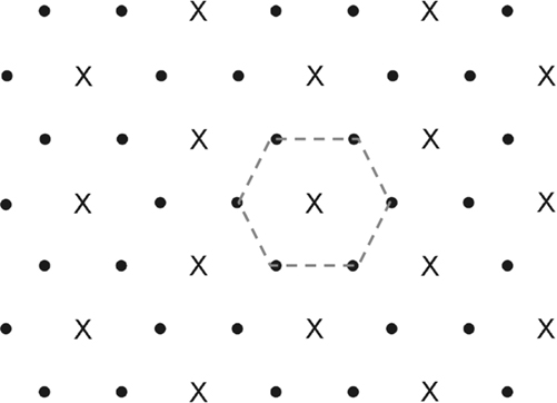
FIGURE 12.3 Si(111) with a saturation coverage of 66% Si–H (dots) and 33% Si–OCH3 (crosses). Si–OCH3 groups block all nearest neighbor atoms (denoted by hexagon) by the 360° thermal rotation of the methyl group about the Si–O bond. Adapted from Ref. 28.
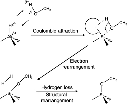
FIGURE 12.4 Proposed mechanism for the methoxylation of the H–Si(111) surface in neat methanol. The mechanism produces H2 and necessitates no free carriers from the bulk Si. Reproduced from Ref. 46 by permission of the American Chemical Society, © 2006.
The barrier height can be correlated with the metal work function, though the dependence is weak (Fig. 12.5).
An important exception is the formation of Si/Hg junctions [26,57–59]. Si/Hg silicides do not form under ambient conditions, as has been shown via XPS [59]. Hence, the Si/Hg junction has proven to be an important tool for soft-contact, nondestructive, electrical characterization of Si surfaces. Impedance spectroscopy and current density versus voltage (J–V) data have shown that the Si/Hg junction is near ideal, in contrast to other metal/Si junction formation schemes.
12.2 REACTIVITY OF HALOGEN-TERMINATED SILICON SURFACES
12.2.1 Background
Halogen-terminated silicon, that is, Cl–Si, Br–Si, and I–Si, has been studied extensively because halogen etching and termination was, initially, integral to understanding the reconstructions of Si(111) and Si(100) surfaces [60,61]. This work was all performed under UHV conditions, with UHV-cleaned Si and molecular gases. Later it was discovered that Si surfaces in contact with Br2/ROH or I2/ROH solutions displayed very low surface recombination velocities [27,62–64]. While neither the surface-bound species nor the mechanism for the surface lifetime enhancement was known, this behavior sparked much interest, and motivated research in the field. Finally, more recent interest in halogenated silicon surfaces has been spurred because although the halogen-terminated surfaces are more reactive than H-terminated surfaces, they can nevertheless be handled briefly under ambient conditions [65]. Accordingly, the halogenated Si surfaces serve as convenient and scalable intermediates for the solution-state syntheses of bound organic monolayers [66–70], and as a reactive surface for the deposition of inorganic films via atomic layer deposition (ALD) [71–75].
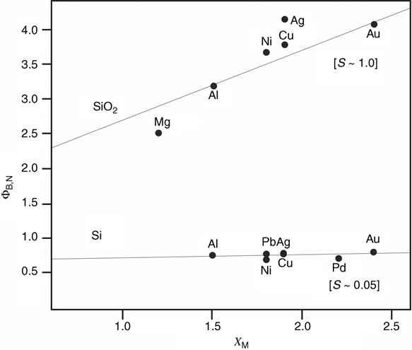
FIGURE 12.5 Barrier height at Si/metal and SiO2/metal junctions as a function of the metal electronegativity. The slope, S, is inversely related to the extent of Fermi level pinning, where an ideal junction would have S = 1.0. Adapted from Ref. 56 by permission of the American Physical Society, © 1969.
This section will focus primarily on the reactivity of halogenated surfaces in environments, for example, air, water, and organic solvents, that are typically encountered when the surfaces are used as intermediates for further functionalization. Many methods can be used to produce each halogenated surface, so a brief discussion of the differences in the resulting halogenated surfaces, and their effect on the subsequent surface reactivity, will also be presented.
12.2.1.1 Synthesis of Cl-Terminated Surfaces
Several methods allow for the synthesis of Cl-terminated Si surfaces, including gas-phase reactions with diatomic molecular halogens under UV irradiation [69,76,77], elevated temperatures [78–80], and room temperature [77,81], in addition to solution-state methods like PCl5 with a radical initiator [67,77,82–86]. These methods have been shown to result in nominally similar Si–Cl surface bonding; however, the coverage, homogeneity, and etch pit density vary for the different functionalization methods and for different crystal faces. The van der Waals radius of Cl is 1.75 Å, so Cl atoms can terminate every atop site on an unreconstructed Si(111) surface [87]. Surface extended X-ray absorption fine structure (SEXAFS) analysis showed that after exposure of Cl2(g) to the reconstructed Si(111)-(7×7) surface, Si–Cl bonds were present and were oriented normal to the surface [88]. Variable-angle FTIR [77], STM [81], and HREELS [81] have also shown that the Si–Cl bonds are normal to the surface on Cl–Si(111) surfaces that have been synthesized from solution-phase or gas-phase reactions of the H–Si(111) surface (Figs. 12.6 and 12.7).
Detailed comparisons have been made between the properties of halogenated Si surfaces prepared by gas-phase and solution-based methods. Room-temperature gas-phase and solution-phase methods both produced Si–Cl bonds with a vibrational peak FWHM of 5 cm–1, as observed via infrared absorption spectroscopy (IRAS) [77]. This narrow peak width indicated extended regions of homogeneous Si–Cl termination. At short Cl2 exposure times, partial Si–Cl coverage was observed without observable roughening of the surface [87]. The chemical shift of the Si–Cl stretching mode was dependent on the Si–Cl surface coverage. A STM study showed that the solution-state method, PCl5 with benzoyl peroxide, was sensitive to the reaction temperature [83]. As the temperature of the reaction increased, so did the density of etch pits. Based on soft X-ray photoelectron spectroscopy (SXPS) data, Si–Cl surfaces functionalized by the room-temperature gas-phase reaction gave comparable Si–Cl coverage to surfaces produced by a solution-state reaction pathway. While the solution-based method resulted in a higher amount of oxygen, 1.4 ± 0.6 ML as observed via XPS, no SiOx was detectable in the SXPS spectra. The presence of oxygen was attributed to solvent workup steps that were not necessary for the gas-phase reaction. IRAS is more sensitive for oxide detection, and based on integration of the 1080 cm–1 peak, gas-phase chlorination gave ~3% of a ML of Si–O–Si, whereas the solution-phase chlorination produced <15% Si–O–Si coverage. In other IRAS studies, very low surface oxidation, 1.2%, or 0.15 ± 0.01 A of subsurface oxide, was observed to form during the solution-phase chlorination reaction [89]. The observed differences in oxidation could thus be due to brief exposure of the surface to ambient air as opposed to the inherent properties of the reaction sequence. Based on vibrational shifts, the oxidation was presumed to be in isolated patches [77]. Despite the difference in etch pit density and initial SiOx coverage, an SXPS study showed that the surfaces prepared by the room-temperature gas-phase and solution-phase halogenation routes oxidized at comparable rates [84]. The initial oxide formation during the Cl termination step did not affect the electronic trap state density at the resulting Si–C terminated surfaces. In fact, CH3CH2– Si(111) surfaces formed from solution-functionalized Cl–Si(111) showed only a slightly higher oxidation after >3 days in air than surfaces made from gas-phase Si–Cl precursor surfaces; however, the SRV after 24 h in air was measured to be lower for surfaces made from the solution-phase route compared to that of the CH3CH2–Si(111) surface formed from gas-phase functionalized Cl–Si(111).
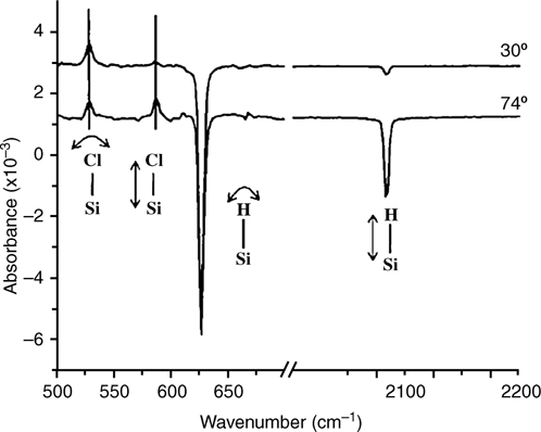
FIGURE 12.6 Transmission FTIR of the Cl–Si(111) surface (referenced to the H–Si(111) surface) produced using a wet chemical technique [77]. Si–Cl and Si–H (subtracted) bend modes are observed at both 30° and 74° off normal. The Si–Cl and Si–H stretch modes are polarization dependent and are observed only at 74° off normal, indicating that these modes are perpendicular to the surface. Reproduced from Ref. 77 by permission of the American Institute of Physics, © 2005.
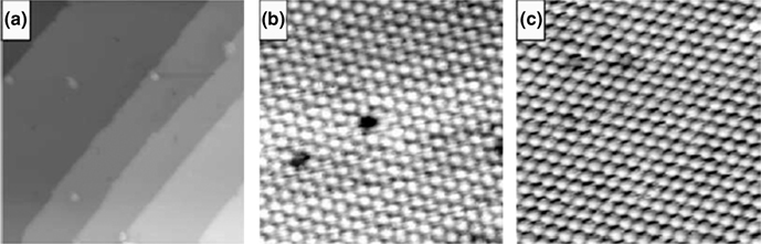
FIGURE 12.7 Constant-current STM images showing full coverage halogenated Si(111) surfaces with little roug hening. (a) Cl–Si(111), 50×50 nm2, –1 V sample bias, 40 pA; (b) Cl–Si(111), 6.5×6.5 nm2, –0.5 V, 50 pA; (c) Br–Si(111), 6.5×6.5 nm2, 0.4 V, 400 pA. Reproduced from Ref. 81.
Differences in Si–Cl surface coverage, and in the surface roughness that resulted from various types of Cl2(g) reactions, were found to be dependent on the reaction conditions. The photoinitiated chlorination of silicon led to broadening and a red shift of the Si–Cl vibrational peaks, suggesting that such Si(111) surfaces were not fully covered with Cl atoms [77]. A change in the temperature of chlorination of Si (100) with UV, from 350 to 423 K, led to an increase in surface roughness, from 1.70 ± 0.54 to 7.9 ± 7.0 Å [90]. The initial H-terminated surface had a roughness of 1.61 ± 0.14 Å. Significant etching by Cl2 occurred only above 350 K and 10 Torr.
The temperature-programmed desorption (TPD) analysis of Cl–Si(111) synthesized via a solution-based benzoyl peroxide-initiated PCl5 route closely matched that of high-coverage, gas-phase functionalized Cl–Si(111), although some differences were observed in the high-temperature desorption [67,82,91]. TPD of high-coverage Si surfaces showed desorption of SiClx, where x = 2 and 3, beginning at 670 K, with some x = 4 and 2 desorbing at 850 K [67] or 950 K [91]. At low Cl coverage, SiCl2 was the main product, and desorbed at 950 K [91]. A recombinative desorption mechanism was proposed, in which Si–Cl + Cl ![]() SiCl2 and SiCl2 + Cl
SiCl2 and SiCl2 + Cl ![]() SiCl3. The Cl-terminated Si surfaces were demonstrated to be stable for >12 h in inert atmosphere [80,92].
SiCl3. The Cl-terminated Si surfaces were demonstrated to be stable for >12 h in inert atmosphere [80,92].
12.2.1.2 Synthesis of Br-Terminated Surfaces
Several methods, including Br2(g) or Br2(soln) and solution-based bromination reagents such as N-bromosuccinamide (NBS), have been used to obtain Br-terminated silicon surfaces [66]. It has been suggested that most of these functionalization methods proceed by the same mechanism. For example, it is thought that the NBS reaction generates in situ small amounts of Br2, which is presumed to be the actual brominating agent. Solution-based bromination has been achieved using NBS in DMF, with a radical initiator present, upon heating to 60° C for 20 min. Bromochloroform can also be used under thermolysis (80°C for 30 min), photolysis (300 nm UV for 30 min), or radical initiation (benzoyl peroxide at 60°C for 30 min) to produce Si–Br terminated Si surfaces [66]. All of these methods produced the same Si–Br shift in XPS and showed C and O present on the surface, attributable to adventitious C and O sources.
12.2.1.3 Synthesis of I-Terminated Surfaces
Unlike Cl- and Br-terminated surfaces, iodine was not observed to terminate every atop site on Si(111), so such surfaces have always been found to be chemically inhomogeneous. Solution-state iodination of silicon surfaces has been accomplished through several methods. Si(001) surfaces functionalized by submersion in I2/benzene gave ~33% coverage of Si atop sites [68]. Surfaces functionalized in this manner showed surface photovoltage effects suggesting the presence of midgap surface states. SEXAFS data of surfaces resulting from the reaction of I2 with the reconstructed Si(111)-(7×7) surface showed that I binds in the same fashion as Cl–Si(111), forming Si–I bonds oriented normal to the Si surface [88].
Exposure of vacuum-cleaned Si(100)-(2×1) surfaces to CH3I resulted in mixed CH3 and I termination [93–95]. Approximately one CH3I adsorbed per two Si atop atoms. The surface was characterized through a variety of techniques, including kinetic uptake measurements [93], TPD [93], Auger electron spectroscopy (AES) [93], HREELS [94], and IRAS [95].
Differences in the reactivity of Cl-, Br-, and I-terminated silicon in air or toward solvent and other reactants have not been thoroughly documented. The different factors that affect etching by molecular diatomic halogens, however, have been well investigated. While measurements of the activation energy for desorption are not statistically different between Si–Br and Si–Cl surfaces, Br potentially has a lower activation energy for desorption from Si than Cl does [96]. The activation energy for desorption of Cl was observed to be 2.3 ± 0.3 eV, while that of Br was 1.8 ± 0.4 eV. In addition, during bromination the higher adsorption probability and back-bond breaking probability should be considered. The adsorption probability was 1.7 times that of Cl, and the back-bond breaking probability was 2.5 times that of Cl.
Finally, caution is advised in interpretation of some data for halogenated surfaces. Br–Si bonds were observed to break during Rutherford backscattering (RBS) and AES experiments [97]. In addition, while monochlorinated sites were stable under UV illumination, dichlorinated sites were not [90].
12.2.2 Reactivity of Halogenated Silicon Surfaces
12.2.2.1 Halogen Etching
When clean, reconstructed Si surfaces or H-terminated Si surfaces are exposed to diatomic halogens, etching can occur, leaving a halogen-terminated surface [60,61,72,77,92]. Alternatively, exchange of hydrogen for halogen termination on H-terminated Si surfaces occurs [61,80,92]. Both of these mechanisms result in a halogen-terminated Si surface; however, the choice of reaction conditions dictates whether the initial surface structure will be preserved. For example, Si is etched upon exposure to HCl in vacuum at high temperatures, but at lower temperatures, HCl exposure results in Si–Cl termination [79].
Solution-based Cl termination of Si via radical-initiated PCl5 (~0.7 M PCl5 in chlorobenzene with a catalytic amount of benzoyl peroxide) results, by STM, in an increased density of etch pits relative to functionalization at room temperature with Cl2(g) [83]. The density of etch pits was dependent on the reaction temperature. IRAS was used to characterize surfaces functionalized via the solution method, and the Si–Cl stretch (586 cm–1) and bend (626 cm–1) were observed [89].
12.2.2.2 Aqueous Media
Exposure of Cl-terminated Si to 2 Torr of pure water vapor for 1 h, did not lead to surface degradation. HREELS showed some peak broadening, but upon heating to 100–200°C, the original spectrum was restored [81]. After vapor exposure and heating, no reaction, or adsorbed species, were observed via HREELS or STM. A more in-depth study focused on the effect of temperature during water vapor exposure [98]. IRAS was used to monitor the reaction of D2O at Cl–Si(111) and Cl–Si(100) surfaces. At T<300°C, no reaction was observed. At >300°C, Si–Cl modes diminished and a broad feature, indicative of Si–O–Si, grew in at 1050 cm–1. The Si(100) surface was less stable, with oxidation apparent at 250°C. With increasing temperature, the oxide modes observed on Cl–Si(111) split into the transverse optical (TO) and longitudinal optical (LO) modes of an extended SiO2 structure at 1060 and 1240 cm–1 (Fig. 12.8). A 1 min exposure to D2O at 450°C resulted in an overlayer having ~1/3 of the thickness of a native oxide, that is, 5.5 Å of oxide. No O–D stretch was observed at any temperature tested, for a 1 min D2O exposure. After D2O expose and an additional 15 min heating period, additional oxidation and the appearance of a peak at 2760 cm–1 were observed. It was presumed that additional reaction with physisorbed D2O effected the increase in overlayer thickness to 8.6 Å of oxide and 0.5 ML of Si–OD. Reaction of Si–Cl with H2O vapor was not a viable method to form oxide-free, OH-terminated Si, because the temperature required to produce Si–OH also caused oxidation of the Si surface.
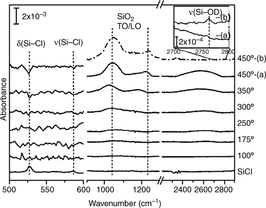
FIGURE 12.8 Transmission FTIR spectra of pure D2O exposure to Cl–Si(111) surfaces at increasing temperatures. Below 300°C, no reaction is observed; however, at greater than 300°C, Si–O–Si stretching modes at 1050 cm–1 appear. O–D stretch modes are not observed at any temperature after a 1 min exposure without a 15 min anneal at T=450° C. Reproduced from Ref. 98 by permission of the American Institute of Physics, © 2005.
Immersion of Cl–Si in water that contained pyridine, or even a 5 s dip in pure water, resulted in irreversible oxidation of the surface. After immersion, hydroxide termination, with a peak at 825 cm–1, with O insertion into the Si–Si back-bonds, with a peak at 1120 cm–1, was observed via HREELS [81] (Fig. 12.9) and via IRAS [80]. The Si–Cl vibrational peak intensity also diminished. Surface hydroxylation is of interest as a starting surface for ALD; however, this method does not lead to a hydroxylated surface that is free of back-bonded O. The inversion layer, created by the electron-withdrawing chlorine at the Si surface [92], decreased when the surface was immersed in H2O [81], as evidenced by a narrowing of the elastic peak observed by HREELS. AM1 Si cluster models showed that Si– Cl bonding was preserved, with O insertion into back-bonds, and concomitant H2 production, as the thermodynamically favored reaction pathway (Fig. 12.10). Cl-terminated Si has been used as an intermediate in the deposition of SiO2 by ALD. The two-step growth process uses H2O and SiCl4 [71,99]:
(a) Si–OH* + SiCl4 → SiO–SiCl3* + HCl
(b) Si–Cl* + H2O → Si–OH* + HCl
where * denotes a surface species. The growth was slow and required large amounts of H2O and high temperatures, likely because of the low reactivity of Si–Cl with water vapor. Upon addition of pyridine, however, the temperature required for growth decreased from >600 to 300 K, and the saturation exposure of H2O was reduced from~109 to~104 L [71]. It was suggested that pyridine complexes with the H of the surface Si–OH moieties, allowing for nucleophilic attack of the SiCl4.
Br-terminated Si is not stable in fluoride-containing aqueous solutions. The fluoride etch acts by attacking the polarized Si back-bonds, and completely removes Br from Br-terminated silicon surfaces [97]. It is very likely that an analogous process would be observed for Cl- and I-terminated surfaces.
12.2.2.3 Oxygen-Containing Environments
The Cl-terminated Si surfaces are relatively stable in air, compared to the air stability of a vacuum-cleaned Si surface. Transport in air for up to several minutes does not lead to observable surface contamination [83]. The conductivity of Si–Cl surfaces decayed rapidly upon continued exposure to air, with decay time constants of <15 min or >1 h, depending on the humidity [92]. The Si:Cl ratio of such surfaces calculated by XPS decreased by 50% after 20 min in air [100]. Upon exposure to air for extended periods of time (>15 min), oxidation was observed at Cl-terminated Si surfaces via IRAS and HREELS [80,81]. After 1 h in air, HREELS spectra showed clearly visible peaks at ~1110 and 850 cm–1, which indicated back-bonded O in a relatively advanced state of oxidation. This behavior indicated that the oxidation occurred in patches. Unlike the oxidation resulting from immersion in water, air oxidation led to very few hydroxylated Si surface sites. Instead, O insertion into back-bonds was observed, with H-terminated Si peaks at 2250 cm–1 (Fig. 12.9). STM images showed that the oxide grew initially at step edges, but upon exposure to air for an extended period of time, the oxide grew in patches that extended from the step edges. After >17 h in air, the surface resembled a “native oxide,” although some Si–Cl sites persisted. After >24 h, Cl was no longer detected by XPS [79]. The contact angle also changed, from 60° to 40°, during oxidation in air. Humidity plays a role in oxidation in air, in that the surface oxidation rate increases as humidity increases. Consistently, the time to degrade the surface conductivity decay increased from 15 min to over an hour with changes in humidity [92]. The factors contributing to oxidation of Si– Cl surfaces in air are complex, and are analogous to those involved in the oxidation of Si–H in air [80]. Water plays a role, but as mentioned earlier, pure water vapor does not cause oxidation. Few studies offer a direct comparison of the stability of different crystal faces of halogen-terminated Si; however, in a comparison of the stability in air of Cl–Si(111) and Cl–Si(100), the (111) surface was more stable [79,80]. The difference in stability was proposed to arise from the chemical inhomogeneity, or only partial chlorination of the Cl–Si(100) [80].
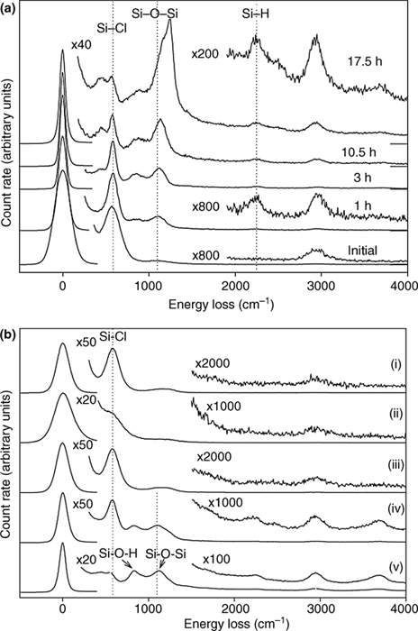
FIGURE 12.9 (a) Oxidation of Cl–Si(111), observed using HREELS, by exposure to air for various times. (b) HREELS spectra of Cl–Si(111) (i), after exposure to 7×10⁹ L water vapor (ii), after water vapor exposure and heating to ~200°C (iii), 5 s dip in deoxygenated H2O (iv), and water dip for 1 min (v). Figures reproduced from Ref. 81.
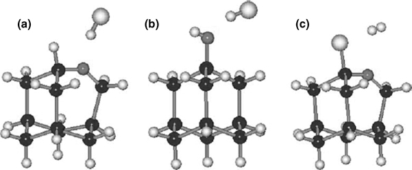
FIGURE 12.10 Possible reaction products from the reaction of the Cl–Si(111) surface with water. (a) Oxygen insertion in the Si–Si back-bond with hydride termination of the Si atop site and evolution of HCl, (b) hydroxylation of the Si atop site with release of HCl, and (c) oxygen insertion in the Si–Si back-bond with H2 evolution and retention of the atop Si–Cl. Reproduced from Ref. 81.
Br-terminated Si(111) has also been reported to be only mildly moisture sensitive and stable in air for up to several minutes [66].
12.2.2.4 Alcohols
Subsequent to the observation of very low SRV values for Si surfaces in contact with I2/MeOH, the reactivity of halogenated surfaces with alcohol was thoroughly investigated. In addition, the surface chemistry of Si in MeOH is interesting because MeOH is a common rinse solvent for solution-phase Si surface functionalization chemistries.
When Cl-terminated Si was immersed in a 0.1 M alcohol solution and heated to 60–70°C for >14 h, alcohols were observed to attach to the Si surface [69]. This method of surface functionalization has been demonstrated on Si(111) and Si (100). On Si(111), the addition of pyridine catalyzed the reaction, although the effect on rate was minimal. XPS analysis of Si– OR surfaces functionalized via this method indicated the presence of some suboxides. After 15 h at 60°C in either octanol or octadecanol, well-ordered organic films were produced on the resultant Si surfaces [79]. The contact angle was observed to increase from 70° on the Cl-terminated surface to >102° for the Si–OR surfaces. An increase in thickness, measured using ellipsometry, corroborated the increase in contact angle after reaction with alcohols. Sonication of Cl-terminated Si in MeOH for 10 min resulted in oxide patches of ≤0.2 Å or 1.6% surface area, and Si–O–C vibrational modes, as detected by IRAS. The consumption of 28% of the Si– Cl sites was observed via RBS [89]. However, in contrast, the same surface investigated by XPS showed no reaction with methanol during sonication at room temperature [82]. The discrepancy in apparent surface reactivity could be due to solvent purity, degree of etching during chlorination, sensitivity of analysis method, or some other factor.
The decrease in SRV observed for Si in contact with Br2 in MeOH or I2 in MeOH was initially proposed to arise from Br and I passivation, respectively. Subsequent work indicated that some Si sites were Br-terminated after immersion in Br2/MeOH, and other Si sites were methoxylated [63]. An increase in SRV was observed after extended time periods, and was attributed to the thermodynamically favored oxidation of Si–Br sites by dissolved O2 or residual H2O.
An XPS comparison of I–Si(100) surfaces functionalized from benzene and from methanolic I2 solutions showed decreased C and higher I coverage on the surfaces that had been functionalized in benzene [68]. Immersion of Si in the I2/benzene solution gave ~33% of a monolayer while I2/MeOH gave only 18%. The decrease in SRV can be attributed to repulsion of carriers from the surface, as a result of band bending induced by the large barrier height contact between the Si and the I2/MeOH solution (Figure 12.2) [27,101]. At longer immersion times, the SRV increased [63], consistent with the thermodynamically favored oxidation of Si–I sites. As the surface oxidized, electronic defect states could pin the Fermi level and decrease the band bending, thus increasing the effective SRV. Upon immersion of H–Si(111) in I2/MeOH, both I- and CH3O–terminated sites were observed [68,102,103]; however, isotope labeling studies showed that the CH3O– termination occurred only during immersion in I2/MeOH, not during a subsequent rinse [102,104]. This suggested that alkoxylation was not occurring through Si–I sites, but via reaction of CH3OH with H-terminated sites, with I2 acting as an oxidant.
12.2.2.5 Other Solvents
Alkylated surfaces formed via the two-step halogenation alkylation reaction were studied using IRAS and RBS [89]. TO and LO (1034 and 1100 cm–1) SiO2 oxide modes were observed after submersion of Cl–Si(111) surfaces in an alkyl Grignard solution at 80°C, and oxidation was thought to occur in patches. Ring opening of the THF, through a mechanism similar to autoxidation with O2 and light, was thought to play a role in the observation of Si–O–C modes (Fig. 12.11). When Cl-terminated surfaces were immersed in anhydrous, inhibitor-free THF at 80°C for 3 h, <25% of the Si–Cl was consumed, and 5 Å (20% of a monolayer) of Si–OR was observed. In another study, Cl–Si(111) was immersed in 1.0 M CH3CH2MgCl in THF-d8 at 70°C, and no C–D was observed via grazing angle ATR [105]. The cause of the discrepancy is unknown, but could be due to impurities. Reemergence of H-terminated sites was observed after alkylation reactions on Cl-terminated silicon [89,105,106]. Isotope labeling studies have shown that the hydride originates from the β-hydrogen on CH3CH2–Si(111) [105]; however, in the absence of a β-hydrogen, H termination is still observed. It has been suggested, although not demonstrated, that this could originate from the solvent [106].
TABLE 12.2 Lifetimes of Si Samples [101]
As with H-terminated silicon, any passage of anodic current on Cl–Si(111) would likely oxidize the Si; however, this expectation has not been borne out by experiment. An irreversible reduction of Cl–Si(111) in THF has been observed at –2.5 V versus Ag/Ag+ [106]. Upon successive sweeps, the intensity of this reduction decreased, indicating that the reducible species was in finite supply at the electrode.
I-terminated surfaces are more susceptible to nucleophilic attack than is the H-terminated silicon surface [68]. Reactivity of I–Si(111) has been observed with terminal olefins in the presence of light. This behavior is in contrast to that of Cl-terminated silicon, which does not react with ethylene, even under UV irradiation [100]. Using this approach, the 2,2,2-trifluoroethyl-undec-10-enoate was attached to I-terminated Si surfaces. This functionalization was reported to be faster, and to occur under irradiation with longer wavelength light, than hydrosilylation of H-terminated silicon. Photopatterning was also demonstrated. Doping highly affected this reaction, suggesting that photo-excited carriers created Si+ sites for attack by a nucleophile.
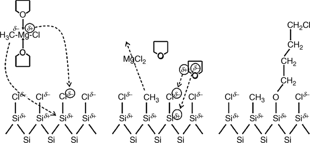
FIGURE 12.11 Proposed reaction mechanism of Grignard reagent addition and THF ring opening at the Si–Cl surface. Reproduced from Ref. 89 by permission of the American Chemical Society, © 2007.
Amine functionalization has been observed on clean Si(111)-(7×7) surfaces in UHV [107]. In addition, amines were observed to react with Cl–Si(100) and porous Cl-terminated surfaces in vacuum at 450 K and in solution with porous Cl-terminated Si [70]. The surface species was thought to be a bridged amine, Si–N(R)–Si, with loss of HCl in the reaction, because no N–H was observed via IR. The amine-functionalized surface was thermally stable up to 750 K in UHV [70]. In another gas-phase example, exposure of Cl–Si(100) to NH3(g), at 348 K and below 100 Torr, produced Si-bound primary amines [90]. Assignment of the surface species was based on the XPS shift of the amine-derived N. Upon heating to 500–1100 K, a transition to secondary and, finally, to tertiary amines was observed (Fig. 12.12). This behavior could explain the observation of secondary amines on surfaces that were functionalized at a higher temperature. A saturating coverage of 0.33 ML of Si–NH2 was observed; this coverage was attained within 5 min and, below 100 Torr, was independent of pressure. The reactivity of Cl–Si(100) with NH3 was markedly different from that of H–Si(100), in that no reaction was observed at H-terminated silicon. The higher reactivity of Cl–Si was attributed to a lower activation energy. At higher pressures, oxidation by H2O contaminants dominated the surface reactivity. Although the bond energy of Si–Cl is very high (3.7 eV versus 2.5 eV of Cl–Cl and 2.3 eV of Si–Si), the Si–Cl bond is very polarized. Incoming ammonia could form a dative bond to Si, facilitating the reaction. First-principles calculations of ammonia adsorption on Cl–Si(001) have shown that reaction with release of HCl is highly thermodynamically unfavorable [108]. It was suggested that a surface bound Si–NH3+ with bound Cl– remaining on the surface is more likely, but experimentally no Si–NH3+Cl– was observed [90].
As would be expected in small molecule chemistry, the presence of an organic base, such as pyridine, promotes nucleophilic attack at Cl-terminated Si (Fig. 12.13).
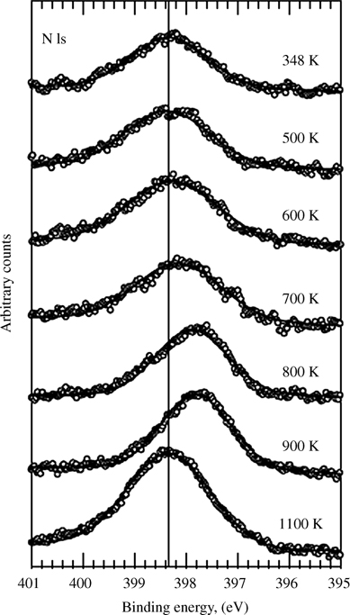
FIGURE 12.12 High-resolution XP spectra of the N 1s peak after exposure of a Cl-Si(100) surface to NH3 (10 Torr NH3 in N2 at 100 Torr for 10 min) at 348 K. Transition from primary to secondary to tertiary amines is observed with annealing at the temperatures indicated. Reproduced from Ref. 90.
Pyridine accelerates the reaction between Cl-terminated silicon and water [81], including water vapor [71], as well as reactions with alcohols [69,109]. Pyridine has also been used to catalyze dense OH-terminated polyethylene glycol (PEG) brush formation on Cl-terminated silicon [109].
12.2.2.6 Metals
Because halogen-terminated Si surfaces are, in general, a reactive intermediate for surface functionalization, X–Si/metal heterojunctions are rare. The Cl–Si(111) and Cl–Si(100) surfaces have been used as starting surfaces for the ALD formation of Al- and Hf-based dielectrics [98]. The resulting surfaces were relatively unreactive with water; however, Si–M bonds were readily formed. After exposure to trimethylaluminum (TMA), Al–CH3 and Si–CH3 modes were readily visible via IRAS.
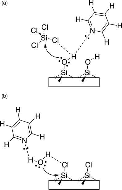
FIGURE 12.13 Proposed mechanism of pyridine activation during the SiCl4 (a) and H2O (b) half-reactions of the ALD growth of SiO2. Redrawn figure adapted from Ref. 71.
12.3 CARBON-TERMINATED SILICON SURFACES
12.3.1 Introduction
The chemical mechanisms of Si–C bond formation have been discussed in the previous chapter. Hence, this chapter focuses on the reactivity between Si interfaces and common reactants, including water under neutral, acidic, and alkaline conditions, ambient atmosphere, metals, and a variety of common organic solvents, including alcohols. The physical and electronic properties of C-terminated Si surfaces are described below, as a starting point to elucidate the effects of reactivity of the Si–C surface under commonly occurring conditions.
The reactivity of Si–H, Si–Br, and Si–Cl surfaces depends on the surface roughness and on the crystal orientation. In addition, for C-terminated Si surfaces, incomplete termination (i.e., a mix of Si– C and Si–H terminated atop sites) and physical barriers imposed by large molecules also affect the surface reactivity. The fully methyl-terminated Si(111)-(1×1) surface (CH3–Si(111)) provides a unique opportunity to obtain detailed insight into the inherent chemical reactivity and electrical properties of the Si–C bond. A comparison between the atop Si atom spacing of 3.84 Å [53] and the van der Waals radius of the methyl group (~2.5 Å) suggests that –CH3 is the only saturated hydrocarbon that can terminate every atop site on the unreconstructed Si(111) surface [85,110,111]. The conversion of atomically flat H–Si(111) to CH3–Si(111), via the Cl–Si(111) surface, produces an atomically flat, CH3–Si(111) surface with nominally unity coverage (Fig. 12.14) [67,85,112]. The CH3–Si(111) surface can also be synthesized through the anodic addition of CH3MgI to H–Si(111) [110]. Because the smallest physical barrier to interacting with the Si–C bond is presented by the CH3–Si(111) surface, its similarities to, and differences from, other C-terminated surfaces will be highlighted.
Isolation of the stability introduced by a physical barrier to reactants is more difficult. The deconvolution of the effects of a physical barrier and chemical stability have been attempted [113]. It is important to understand effects of a physical barrier on stability, as well as the consequences for common applications.
12.3.2 Structural and Electronic Characterization of Carbon-Terminated Silicon
The structural characterization of C-terminated Si surfaces will be briefly reviewed, as it serves to highlight the properties and differences among Si–C terminated surfaces.
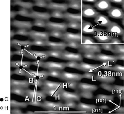
FIGURE 12.14 STM image of CH3–Si(111) surface (4.7 K, sample bias Vs = – 2.5 V, and constant current of 0.050 nA). The center to center distance of the –CH3 groups (L to L′)is 0.38 nm. The low-index planes, denoted in the bottom right, were determined by X-ray crystallography. The surface unit cell is outlined by the parallelogram, with –CH3 groups superimposed at each vertex. The angle between A and C is 7 ± 3°. The inset (top right) is the same surface imaged at 77 K. Figure reproduced from Ref. 112 by permission of the American Chemical Society, © 2005.
12.3.2.1 Structural Characterization of CH3–Si(111)
Two methods have been used to synthesize CH3–Si(111) surfaces [67,110]. One is through anodic addition of CH3MgI to H-terminated Si surfaces [110]. The other, more widely utilized approach, is through surface halogenation followed by alkylation. In the later approach, a highly reactive Si–Cl or Si–Br surface is synthesized and then exposed to alkyl Grignard ororganolithium reagents [67]. The resulting CH3–Si(111) surface has been thoroughly characterized. The chlorination/alkylation procedure results in an unreconstructed Si(111) surface, as evidenced by LEED [114]. The absence of Si–H, Si–O, and Si–Cl stretching modes in the FTIR spectrum of CH3–Si(111), along with the appearance of a polarization-dependent –CH3 umbrella mode, suggested that Si–C bonds terminated every atop Si atom on the unreconstructed Si(111) surface [115]. The polarization dependence of the methyl umbrella vibrational modes showed that the –CH3 group was attached normal to the Si(111) surface plane. The Si–C bond has been directly observed through photoelectron spectroscopy (PES) [85,116], HREELS [82], and FTIR spectroscopy [115]. Surface-sensitive XPS and ultraviolet photoelectron spectroscopy (UPS), in conjunction with use of the substrate-overlayer model, indicated a –CH3 group coverage of one monolayer [85,116–118]. Low-temperature STM images confirmed the high degree of order, and unity coverage, of the CH3–Si(111) surfaces over large-area terraces [112]. Thus, the CH3–Si(111) surface is an ideal surface to understand the effects of kinetic stabilization of the Si–C bond without the confounding effects of the physical barrier imposed by a long-chain alkane or by additional surface functionality.
12.3.2.2 Structural Characterization of Other Si–C Functionalized Surfaces
A large body of literature describes the structural characterization of Si–C surfaces functionalized with groups other than methyl. The reactivities of all such surfaces, aside from CH3–Si(111), are affected by a combination of Si–C site reactivity, non-Si–C functionalized site reactivity, the physical barrier imposed by large molecules, and the terminating chain functionality.
Difference in Coverage
The fraction of saturated C-terminated Si atop sites is nominally unity only for the CH3–Si(111) surface. For all other Si(111) surfaces functionalized with alkanes or alkenes, the Si–C coverage is less than unity because of steric factors. For surfaces functionalized using the two-step reaction or by hydrosilylation, the non-Si–C terminated sites are most commonly terminated by Si–H bonds [105,106,119]. While the CH3–Si(111) surface coverage was measured to be 100% termination of Si atop sites, the C2H5–Si(111) surface had a maximum of approximately 80% coverage [86,120]. As expected, the coverage decreased as the steric bulk of the alkyl group increased [106]. The maximum coverage of surfaces functionalized via hydrosilylation, which commonly employs large molecules, is approximately 50% [111,119]. Clearly, the CH3–Si(111) surface is an attractive choice for the isolation and study of the Si–C bond.
Difference in Coverage Pattern
The hydrosilylation reaction proceeds through a chain reaction on the surface, while for the two-step mechanism each site functionalization reaction is only influenced sterically by closely adjacent sites. The hydrosilylation surface chain reaction therefore leads to patches of functionalization at low reaction conversion (Fig. 12.15) [121]. In contrast, the two-step mechanism is thought to give between random and self-avoiding coverage with bulky functional groups, because of the irreversibility, mechanistic independence, and steric considerations of each reaction event. This difference in mechanism, along with the tendency to proceed to higher coverage, implies that very few adjacent sites are not Si–C terminated on Si surfaces functionalized using the two-step halogenation/alkylation procedure [86,89]. A decreased rate of surface oxidation was observed on partially alkylated surfaces relative to that of Si–H surfaces [122]. It was suggested that if lateral SiOx propagation proceeds through adjacent Si–H sites, the presence of even incomplete Si–C termination would retard the oxide growth. Although clear examples are lacking on the effect of adjacent site identity on surface stability, the degree and identity of non-C-terminated Si atop sites are likely to affect the reactivity of such surfaces.
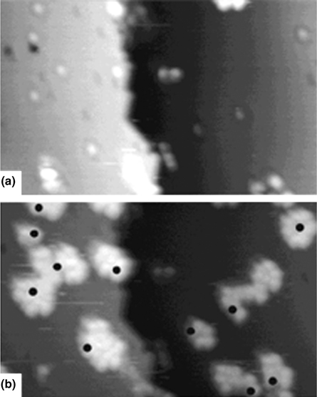
FIGURE 12.15 Occupied state STM images (215 Å × 215 Å, –2.1V, 44 pA) of a H–Si (111) surface with isolated dangling bonds created by desorption activated with the STM tip (a) before styrene addition and (b) after exposure to 12 L of styrene. The black dots in (b) mark the initial dangling bonds showing these sites initiate hydrosilylation of styrene. Maximum height range is ~5 Å (a) and ~10 Å (b). Figure reproduced from Ref. 121 by permission of the American Chemical Society, © 2002.
Difference in Monolayer Density and Thickness
Despite a possible lower coverage of functionalized Si surface sites, an increase in the size of the surface-bound species can also produce a physical barrier on the surface. An increase in the monolayer thickness and density, but not in the total coverage of Si–C bonds on Si atop sites, has been obtained by chemical functionalization of ester-terminated alkane monolayers on Si [113]. This highly protected overlayer increased the stability of silicon toward oxidation under ambient conditions. The monolayer protected the underlying substrate not via kinetic stability of the Si–C bond, but primarily via physical separation between reactant and the silicon surface sites.
Difference in Crystal Face and Surface Roughness
As the density of dangling bonds decreased, either because of surface roughness or due to the structure of a specific crystal face, increased chemical stability has been observed for Si–H and Si–X terminated surfaces [98,123]. CH3–Si(111) surfaces are better passivated toward oxidation in air than are CH3–Si(100) surfaces [124,125]. The unreconstructed Si(100) surface has a higher density of dangling bonds than does the Si(111)-(1×1) surface, 1.36×1015cm–2 compared to 7.83×1014cm–2 on Si (111). Hence, on the Si(100) surface, the Si atop sites are more available forattack by oxidants, because sterically there is not enough space for –CH3 termination of every dangling bond.
Hydrosilylation proceeds to give nominally identical monolayers on Si(111) and Si(100) surfaces [126,127]. TPD results showed similar thermal stability on Si(100) compared to that on Si(111); however, increased disorder of the monolayer was observed via contact angle measurements. The observed behavior is consistent with the increased disorder of the initial H–Si(100) surface, which contained SiH, SiH2, and SiH3 moieties. Although a rigorous comparison of the stability of hydrosilylation-functionalized Si(100) and Si(111) surfaces has not been conducted, a large difference between the two crystal faces may not be present, because the dominant stabilization mechanism for hydrosilylation-functionalized surfaces is a physical barrier, which should be similar on both hydrosilylated crystal faces.
12.3.2.3 Electronic Characterization of Alkylated Silicon
Surface Recombination Velocity
C-terminated Si surfaces, specifically those synthesized via the two-step halogenation/alkylation reaction [67,82], can be prepared with very low electronic defect. The CH3–Si(111) surface exhibited stable SRV values of <40 cm/s for >30 days, in ambient air, despite the growth of some SiOx [67,122,128]. A combination of SXPS and UPS measurements indicated that the low SRV was due to low electronic defect densities rather than due to band bending [114]. Even surfaces functionalized with bulky groups that are capable of only sparse coverage of the Si surface showed SRV values <100 cm/s [106]. These data thus showed that the Si–C bond efficiently passivated the Si surface, and that the electronic properties of these functionalized surfaces were stable in air over long periods of time, unlike the behavior of the Si–H terminated surfaces.
Surface Dipole
The presence of an ~400mV dipole (Fig. 12.16) at the CH3–Si (111) surface has been observed via synchrotron photoemission spectroscopic measurements in UHV. The dipole has been attributed to the electronegativity difference between the C and H of the –CH3 groups [114]. In addition, a comparison of the barrier height measurements made at n-Si–H/Hg and n-Si–CH3/Hg contacts shows an ~0.55 eV dipole [59,129]. In the electrodeposition of Cd and Pb on H–Si versus CH3–Si, the dipole was manifested as the presence or absence of an oxidative stripping peak [130].
Electronic Resistance
An insulating layer between two conducting phases presents a barrier to electron transfer. Experimentally, such a barrier will appear as a series resistance, as has been observed for dense organic monolayers on Si and on other electrode surfaces [132–135]. If the dominant mechanism of electron transfer through a barrier is tunneling, the observed electron-transfer rate constant, k, should depend on the thickness of the barrier, as given by
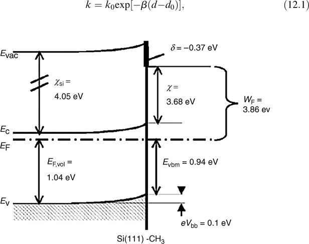
FIGURE 12.16 Energy-band diagram of the CH3–Si(111) surface. The electron affinity, X, of CH3–Si(111) was measured as ~3.7 eV via photoemission spectroscopic measurements, indicating the presence of a surface dipole, 5, of ~400mV. The Si is near flat-band conditions, eVbb = 0.1 ± 0.1 eV, at the CH3–Si(111)/vacuum interface. Figure reproduced from Ref. 114 by permission of the journal article authors.
where k0 is the rate constant in the absence of a tunneling barrier, b is the material-dependent electron tunneling constant (~1.0 Å–1 for saturated alkanes) [136–138], and (d – d0) is the thickness of the barrier. Interestingly, this relationship predicts that electron-transfer rates across Si-bound monolayers should also be highly dependent on the identity of the molecules [59]. A chain length-dependent series resistance was observed for the photoelectrochemical systems Si(111)–CxH2x+1/Me2Fc0/+ (CH3OH) and Si(111)–CxH2x+1/K3Fe(CN)6/K4Fe(CN)4(aq), where x = 1 – 6 [131,139]. The expected exponential dependence of the electron-transfer rate on chain length was not observed (Fig. 12.17), so it was suggested that solution redox couples could penetrate to some extent into the alkyl monolayers [140].
Low interfacial resistance is important for surface electrochemical stability, as well as for device efficiency. The branching ratio of Faradaic current associated with hole transfer to Fe2+, and that associated with oxidation of Si, was altered by introducing a resistive interfacial element in the form of the alkylated overlayer. Ultimately, rapid anodic oxidation of the Si substrate was observed in the presence of very resistive monolayers [139].
12.3.3 Reactivity of C-terminated Silicon Surfaces
Functionalization of Si with the two-step halogenation/alkylation reaction, or through anodic deposition, can produce surfaces with short alkyl chains (≤C4). These two mechanisms, in addition to hydrosilylation and cathodic deposition of diazonium compounds, can also produce surfaces that have thicker organic monolayers. Electrochemical [139] and electroless [106,122,125] stability experiments with shorter chains suggest that higher coverage improves the resulting surface stability. However, electroless experiments on longer alkyl chains (>C6) showed that surfaces with a thicker organic monolayer are more stable [113]. These results seem contradictory; however, a higher degree of disorder is observed in short-chain monolayers, such that small oxidizing agents, like water, could more easily penetrate such barriers. In this regime of oxidizing agents close to the surface, the total coverage of Si atop sites that have a kinetically stable Si–C bond is very important. On the other hand, with thicker organic monolayers, the long-chain alkanes are more ordered, and are better at physically blocking oxidizing agents from the surface. These surfaces also all have nominally the same total coverage, so it is expected that the stability of such systems would increase with the overlayer thickness. A difference was also observed between stability in electrochemical and electroless experiments. In experiments where Faradaic current is passed, the additional resistance that is imposed by an organic monolayer can affect the stability of the resulting surface.
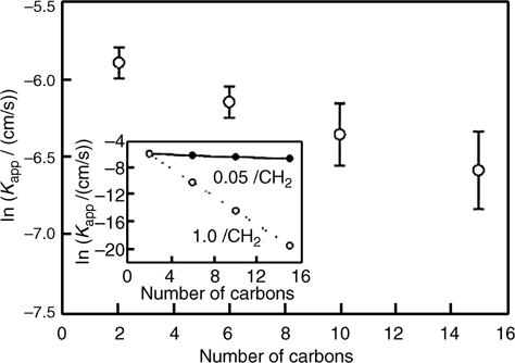
FIGURE 12.17 Plot of the kapp versus alkyl monolayer chain length specified as the number of carbons, n. kapp values were determined from the reduction wave of the cyclic voltammograms based on a convolution integral. The inset shows the measured dependence on chain length, γ = 0.05 CH2–1, in comparison to the prediction assuming β=1.0 CH2–1. Taken from Ref. 140.
12.3.3.1 Thermal Stability of Alkylated Silicon
The thermal decomposition mechanism, and thus the thermal stability of alkylated Si surfaces, depends on the length of the alkyl chain. CH3–Si(111) surfaces are stable up to at least 440°C, but CH3CH2–Si(111) surfaces decompose at <300°C under UHV conditions [120,141]. The thermal stability of CxH2x+1–Si(111) surfaces decreases with increasing chain length, but plateaus at >C6 [141]. Upon heating of surfaces functionalized with >C2 to over 300°C in UHV, Si–H moieties were observed. The suggested mechanisms of desorption included β-hydride elimination, to leave Si–H, and a minority reaction that results in C–C bond cleavage, to leave CH3–Si [120,142,143]. These reactions were found to occur at 250–300°C, while the subsequent desorption of the remaining CH3–Si occurred at higher temperatures. These findings highlight the unique thermal stability of the CH3–Si(111) surface. Under ambient pressure, heating without surface oxidation has proven difficult, and even in nominally reducing environments, Si in higher oxidation states is observed [141].
12.3.3.2 Stability in Aqueous Conditions
Neutral Aqueous Conditions The Si–C terminated surfaces are stable in neutral, O2-free, H2O. Initially, this behavior was tested by immersion of surfaces functionalized by hydrosilylation into boiling H2O for 1 h. Integration of the C–H stretching region using IRAS indicated that the monolayer remained intact. However, the ~30% of a monolayer thought to be tethered through a Si–O–C bond was hydrolyzed [144]. This observation is consistent with contact angle measurements, XPS, AFM, and ellipsometry data that have indicated less than 24 h stability when silanes bonded to oxidized Si surfaces are immersed in water [145,146]. In contrast, immersion of Si surfaces thought to have no Si–O–C bonds into boiling water for 1 h and then room-temperature water for 3 days produced no effect on the observed surface IR vibrational mode intensities [147]. Furthermore, in the case of C18H37–Si(111), immersion into boiling water for 7 h resulted in negligible SiOx formation [119]. When comparing C10H21–Si(111) to EtOOCC10H20–Si(111) to a thicker and more dense, branched (C5H11)2C(OH)C9H18–Si(111) surface, HREELS, contact potential, and differential capacitance measurements all indicated that more dense monolayers led to less SiOx formation and to improved stability [113].
When passing anodic current across the Si/H2O junction, a high concentration of electron-deficient sites (holes) is formed. This process, in the presence of good nucleophiles (H2O, OH−), leads to rapid SiOx formation. Notably, under such conditions, Si–H terminated surfaces are extremely unstable, but Si–C terminated surfaces are remarkably stable [139]. Specifically CH3–n-Si(111) and C2H5– n-Si(111) can sustain photoanodic current densities of 1 mA/cm2 for over 60 min in aqueous solutions with negligible change in open-circuit voltage (VOC) or fill factor, indicating negligible formation of surface states or SiOx. For longer chains, >C4, the photoelectrode performance decayed within the same 60 min time period, although the decay occurred much less rapidly than that of Si–H terminated surfaces. This behavior is consistent with the hypothesis that the additional resistance imposed by the organic monolayer affected the branching ratio of productive to deleterious Faradaic processes (Fig. 12.18).
The Si–C termination not only passivated the Si surface toward oxidation, but also stabilized the band-edge positions as the pH was changed. A pH dependence of band-edge positions is a classic phenomenon observed for metal oxides in H2O, and has also been reported for Si. It was suggested that the Si oxide protonation/deprotonation equilibrium shifts the Si band-edge positions. With pH, however, such shifts are minimal for Si–C terminated surfaces, and were shown to be correlated with the fraction of atop Si sites terminated by C. The reduction of MV2+/•+ (methyl viologen), a pH-independent and water-soluble redox couple, at methyl-terminated n-Si(111) surfaces was in fact shown to be essentially independent of pH [148].
Acidic Aqueous Conditions
Hydrogen-terminated Si is stable in concentrated acids, in the absence of oxidants [2]. C-terminated Si surfaces also exhibit good stability in aqueous acidic conditions. HREELS data have shown that surfaces functionalized with long alkyl chains via hydrosilylation remained intact after 7 h in 0.1 M H2SO4 [113]. In fact, dilute solutions of acids, such as HCl(aq) and trifluoroacetic acid (TFA) in THF, are routinely used to clean Si surfaces after functionalization, or to carry out secondary functionalization reactions [110,126,149]. Organic monolayers have even been shown to resist exposure to very concentrated and/or corrosive acids, like pH 2 H2SO4 for 2.5 h with no detectable oxide growth via XPS [82] or boiling 2.5 M H2SO4 in 10% water in dioxane [119]. In addition, the photoanodic performance of such Si surfaces was not affected by operation at pH 1.5 [148].
Very concentrated acids have been observed to disrupt the Si–C monolayer. Immersion of CH3–Si(111) surfaces in 36 M H2SO4 gave very low SRV values while the crystal was submerged; however, upon a second exposure to ambient air, the carrier lifetime decayed rapidly, suggesting that the monolayer had been damaged [128]. Thorough investigations of the stability of Si–C monolayers in dilute, oxidizing acidic conditions are still warranted, however.
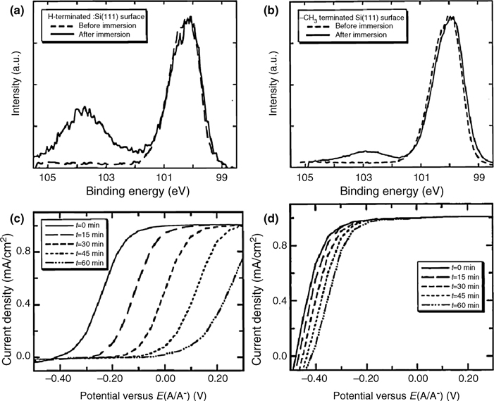
FIGURE 12.18 High-resolution XP spectra of the Si 2p region of H–Si(111) (a) and CH3–Si(111) (b) surfaces before and after immersion in 0.35 M K4Fe(CN)6–0.05 M K3Fe (CN)6(aq) solution for 10 min. The CH3– Si(111) surface is better passivated toward SiOx growth. Time-dependent J–E behavior of H–Si(111) (c) and CH3–Si(111) (d) surfaces in contact with Fe(CN)3–/4–(aq) solution. J–E data were collected at a scan rate of 50mV/s in a three-electrode configuration versus a Pt wire reference electrode poised at the Nernstian potential of the redox couple, E(A/A–). Figures reproduced from Ref. 139 by permission of the American Chemical Society, © 1998.
Fluoride-containing aqueous acidic solutions are known to etch Si slowly, and have been shown to have little effect on oxide-free, Si–C terminated surfaces. The presence of silicon oxide species enabled partial removal of the Si–C monolayer, and fluoride-containing solutions were therefore used to quantify the oxidation of the silicon substrate [82,119,134,147]. Differences in monolayer characteristics have been studied by observing the effects of HF(aq) solutions on the Si substrate. C10–Si (111) functionalized surfaces synthesized via the chlorination/alkylation route or by photochemical hydrosilylation were more robust to immersion in NH4F following 1 h in boiling water than those made via Lewis acid-catalyzed hydrosilylation [147]. The increased stability was attributed to a higher surface coverage, giving more dense organic monolayers in the more stable systems.
Aqueous Alkaline Conditions
While concentrated acids are known to preserve the H-terminated Si surface, alkaline solutions are known to etch Si. Alkaline conditions have been used for secondary functionalization of Si–C surfaces, and a lack of reactivity toward OH− was used as a means of deducing the presence of covalent linkages between alkyl groups and Si surfaces. For example, Si–C terminated surfaces have been subjected to aqueous 10% NH4OH, to effect hydrolysis of ester-protected monolayers, without significant disruption of the surface Si–C bond [150]. Several examples of Si–C terminated surfaces exhibiting a lack of reactivity toward base, with subsequent electronic and structural characterization detailing both the stability of the monolayer structure and the passivation of the Si surface toward oxidation, will be discussed below.
Cathodic biasing of H-terminated n-Si(111) surfaces in buffered pH 11 MV2+ solutions has been shown to lead to significant silicon oxide formation. In contrast, CH3-terminated n-Si(111) surfaces displayed no electrochemical evidence of oxide formation (Fig. 12.19), and significantly less oxide formation was observed by XPS on Si–C terminated Si than on H–Si(111) surfaces [148].
Hydrosilylated Si surfaces have shown stability to immersion in boiling 1 M NH4OH in a 10% water/90% dioxane solution, but showed significant damage after 1 h in boiling 1M NaOH in 10% water/90% dioxane [119]. Organic monolayers synthesized via Grignard reagents or via photochemical hydrosilylation showed a 6% drop in the IR C–H stretching absorption intensity after 10 min in 2M KOH (Fig. 12.20) [147]. XPS data on C12H25–Si(111) surfaces showed the growth of 0.5 ML of SiOx after immersion in pH 13 KOH solutions, but showed almost no change in Si–C coverage, suggesting oxidation, but not etching, of the silicon [82].
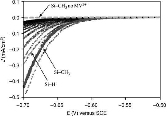
FIGURE 12.19 J–E behavior of H–Si(111) (open circles) and CH3–Si(111) (filled circles) upon repeated cycling in the dark at 10 mV/s in contact with a 10 mM MV2+(aq) solution buffered at pH 11.0. The dark J–E behavior of the CH3–Si(111) surface in contact with aqueous solution with no MV2+ present is shown for comparison (dashed line). Reproduced from Ref. 148 by permission of the American Chemical Society, © 2006.
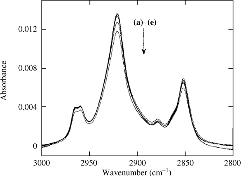
FIGURE 12.20 FTIR spectra of the alkyl C–H stretching region of C10H21–Si(111) prepared via Grignard reaction with a H–Si(111) surface. (a) As prepared followed by a trichloroethane rinse, and through sequential treatment of (b) sonication in CH2Cl2 for 1 min and boiling in CH3Cl for 1 h; (c) boiling in H2O for 1 h; (d) immersion in 40% NH4F(aq) for 10 min followed by 3 days in H2O; (e) immersion in 2 M KOH for 10 min. The integrated area progressively decreases through each treatment. Figure reproduced from Ref. 128 by permission of the American Institute of Physics, © 2000.
An increased monolayer thickness resulted in an increase in monolayer stability in the presence of NaOH(aq). Although the monolayer remained intact after immersion in NaOH, the underlying Si was still subject to oxidation, although much less so than unprotected Si [134]. The passivating properties of Si–C termination also extend to porous silicon [151]. In summary, C termination of Si atop sites impedes Si oxidation and dissolution in aqueous alkaline solutions, due to both the kinetic stability of the Si–C bond and the physical barrier presented by the monolayer.
12.3.3.3 Stability of Si–C Terminated Surfaces in Air
C termination of Si surfaces significantly improves passivation toward SiOx formation in ambient air compared to the behavior of H-terminated Si surfaces. For surfaces functionalized via a two-step chlorination/alkylation procedure, the rate of SiOx formation correlated with increased steric bulk [122]. For example, after 12 h in air, CH3–Si(111) surfaces had formed 0.08 ML of SiOx, C2H5–Si(111) had formed 0.27 ML of SiOx, and C6H5CH2–Si(111) had formed 0.52 ML SiOx. This behavior was attributed to differences in the Si– C bond coverage on the various functionalized Si surfaces. Si–C termination has been shown to decrease the rate of oxidation on a time scale of weeks [122,125]. The carrier lifetime at CH3–Si(111) remained high, 300 ms, even after 1 month of exposure to air, despite the growth of some oxide [128]. A similar result was observed with surfaces functionalized by the reduction of aryl diazonium salts, with surfaces showing growth of 0.5 ML of SiOx within 10 days, but no additional oxidation for greater than 6 months [134,152]. C6H13–Si(111) and C6H13–Si(100) surfaces, synthesized via hydrosilylation, were exposed to air for over 4 months without any detectable growth of silicon oxide via XPS [153].
Multiple factors can impede oxide growth. Oxidation in air has been shown to proceed inhomogeneously at surfaces functionalized via the two-step halogenation/alkylation reaction [122]. The observed oxide was mostly composed of Si+ and Si3+, with negligible presence of Si4+ moieties. Considerable Si4+ was detected at Si–H and Si–Cl surfaces within 1 day (Fig. 12.21). Propagation of oxidation has been hypothesized to proceed though adjacent Si–H or Si–Cl sites, so that even a moderate Si–C coverage would significantly impede long-term oxidation to the Si4+ state. For surfaces functionalized with short-chain alkanes, <C6, it is unlikely that the resistance to oxidation in air is due to the physical blockage of oxidants or else the stability of C2H5–Si(111) would be improved over that of CH3–Si(111). The disorder of short-chain monolayers, known to exist for C2H5–Si(111) [86], thus prevents the monolayers from acting as a significant physical barrier to reactants.
12.3.3.4 Stability of Si–C Terminated Surfaces in Alcohols
H- terminated Si surfaces yield excellent photoelectrochemical performance in methanolic electrochemical cells, but H–Si termination is not stable in methanol [28]. Current density versus potential measurements showed that alkylated n-Si(111) electrodes in contact with CH3OH–Me2Fc+/0 yielded very similar J–V properties to hydride-terminated n-Si(111) electrodes. Differential capacitance versus potential data yielded very similar barrier heights for the two systems. No significant surface recombination was observed; however, the alkyl monolayers did impose additional series resistance to charge transfer at the Si/liquid junction [131]. C-terminated Si proved to be more stable than H-terminated Si upon addition of 20% (v/v) H2O in MeOH. Within 90 min of photoanodic activity, a highly resistive layer had formed on hydride-terminated n-Si(111) surfaces, but alkylated n-Si(111) continued to perform well until the experiment was arbitrarily ended 22–25 h later (Fig. 12.22). Si–H and Si–Cl sites at surfaces with less than complete Si–C termination were susceptible to the formation of alkoxy surface species [89,153,154].
12.3.3.5 Stability in Other Common Solvents
Little information is available on the inherent Si–C bond in common organic solvents, and many solvents and reactants have been used successfully together with Si–C functionalized surfaces [126,149]. In early work, a decrease in C–H stretching intensity was observed after boiling alkylated Si surfaces in CHCl3 for 2 h, but this behavior is now thought to have been due to cleavage of Si–O–C bonds [119,144]. Subsequently, boiling or sonication in organic solvents, such as CHCl3, has shown >90% of the monolayer retention, as determined via XPS and IR [82,147]. The functionalized Si surfaces were less stable at high temperatures, and the contact angles decreased after boiling C18H37–Si(111) in toluene at 111°C for 4 days [153]. Instability of the Si–C functionalized surfaces in organic solvents has sometimes been attributed to the presence of water. Acetonitrile was more harmful to Si–C functionalized surfaces than DMF. This observation was attributed to the greater difficulty in removing trace water from acetonitrile than from DMF [113].
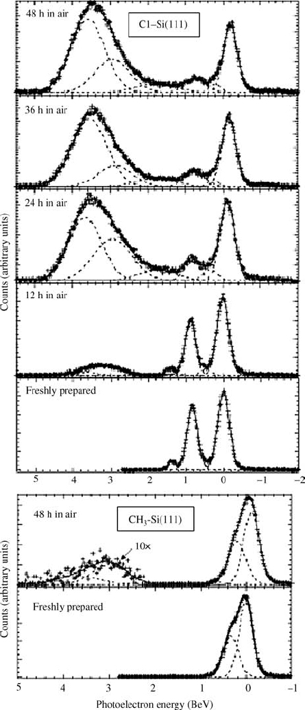
FIGURE 12.21 Time-dependent soft X-ray photoelectron spectra of Cl–Si(111) and CH3–Si (111) surfaces with exposure to air. Spectra are shown after background removal, spin-orbit stripping, and peak fitting. Cross marks are raw data and dashed lines are fits. Note the appearance of oxidized Si signals after shorter exposures to lab air in the Cl–Si(111) spectra. In addition, higher oxides are observed at Cl–Si(111) surfaces than CH3–Si(111) surfaces after exposure to air. Figures reproduced from Ref. 122 by permission of the American Chemical Society, © 2006.
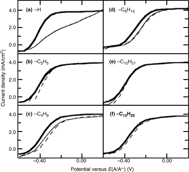
FIGURE 12.22 J–E behavior at H–Si(111) and CxH2x+1–Si(111) functionalized surfaces in contact with CH3OH–1.0M LiClO4–0.050M Me2FC–~1mM Me2Fc+PF6 containing 20% (v/v) H2O. The thick solid line denotes the initial J–E behavior observed immediately after adding water to the electrolyte solution. The thin solid line denotes the J–E behavior after 90 min of illumination at JSC = 4.0 mA/cm2, and the dashed line denotes the J–E behavior after 22–24 h of illumination. Figures reproduced from Ref. 131 by permission of the American Chemical Society, © 1998.
12.3.3.6 Silicon-Organic Monolayer-Metal Systems
Metal silicides are produced at most metal/silicon contacts, and this holds true for most metal/CH3– Si junctions as well. Evaporation of metals such as Au or Cu onto CH3–Si(111) led to silicide formation and Fermi level pinning; however, the –CH3 group affected the formation of the silicides [155]. For Au evaporation onto a bare Si(111)-(7×7) surface, SiAu3 formation was observed at any amount of evaporated Au. However, on CH3–Si(111), silicide formation occurred only at ≥0.5 ML of Au. Partial disruption of the CH3–Si(111) monolayer was observed despite protection of the Si surface. Si/Au barrier heights remained unchanged from those observed on the pinned Si (111)-(7×7) surface. Very similar observations were made for Si/Cu junctions (Fig. 12.23); Cu silicide was observed on CH3–Si(111) surfaces after ≥2 ML of Cu was deposited. Again, silicide formation was observed after any deposition of Cu on the Si(111)-(7×7) surface. Evaporated Cu contacts on the CH3–Si(111) surface also gave barrier heights that were identical to those of evaporated Cu on Si(111)-(7×7). One difference between Au and Cu evaporation was that the SiCu3 remained buried at the Cu/Si interface, rather than floating atop the deposited metal film, as in the case of Au deposition.
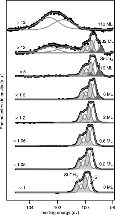
FIGURE 12.23 XP spectra (Eex=150 eV) of Cu deposition onto the CH3–Si(111) surface. Intensities have been scaled as indicated. Contributions from the bulk Si0, CH3-bound surface components (Si–CH3), and copper silicide (SiCu3) are noted. Taken from Ref. 155.
There have been attempts to produce “softer,” less destructive evaporated contacts on semiconductor surfaces. GaAs, which is also commonly limited by Fermi level pinning, was contacted using indirect, collision-induced, cooled electron beam evaporation. This did not solve the problem of metal atom diffusion into the material, but did limit deleterious surface reactions with incoming metal atoms or clusters [156]. A second example of indirect metal evaporation on silicon was the lift-off, float-on (LOFO) technique, in which a metal film was evaporated on a glass slide. The film was undercut through etching of the glass, to leave a very thin, floating metal film that was then transferred to a Si surface. This method could be used without apparent disruption of an octadecyltrichlorosilane self-assembled monolayer, although contact reproducibility was an issue [157].
Hg/Si junction formation proceeds without interfacial silicide formation. Hg/H–Si(111) junctions showed barrier heights consistent with the electron affinity of Si and the work function of Hg: 0.3 eV at H-terminated n-Si(111) and 0.8 eV at H-terminated p–Si(111) (Table 12.3). Neither of these surfaces showed any evidence of reaction with Hg. Capacitance versus voltage (C-V) and current density versus voltage (J-V) measurements of CH3–Si(111)/Hg junctions confirmed the presence of an interfacial dipole, of approximately 0.55 eV compared to that of H–Si(111), attributable to the –CH3 group. n-Si/Hg gave very high barrier heights of 0.91 eV, and p–Si gave practically ohmic contacts [59].
CH3 termination of Si surfaces allows further freedom in Si/metal junction formation. High-quality, unpinned Au/Si junctions were formed on CH3–Si(111) surfaces though dispersion and sintering of butanethiol-capped Au nanoparticles. For H–Si, this scheme led to ill-defined interfacial reactions giving highly resistive barriers (Fig. 12.24) [158]. As previously mentioned, the electrodeposition of Cd and Pb on CH3–Si(111) gave much higher solution/Si and metal/Si barrier heights, as evidenced by lowered oxidative stripping of the deposited metals. In addition, much fewer nucleation sites are present at the CH3–Si(111) surface relative to the H–Si (111) surface. Both Cd/Si and Pb/Si junctions formed by electrodeposition gave high barrier heights, of ΦB~0.8 eV, at CH3–n-Si(111), whereas at H–n-Si(111) the junctions gave ΦB ≤ 0.4 and 0.59 eV, respectively [130].
12.4 APPLICATIONS AND STRATEGIES FOR FUNCTIONALIZED SILICON SURFACES
The previous three sections have explored the stability and reactivity of H-, halogen-, and C-terminated silicon surfaces. Compared to UHV-cleaned surfaces, these functionalized Si surfaces all exhibit remarkable stability. However, Si-based devices made today are expected to last for 10–20 years of operation under ambient conditions. The only surface that yields close to that sort of performance is the C-terminated Si surface. In this final section on Si, we discuss strategies to utilize organic monolayers on Si to further enhance the surface stability during device fabrication and operation.
A very old technique for surface stabilization is the facilitation of charge transfer to turn over productive electrochemical events. This is the final of three surface stabilization techniques presented in this chapter: kinetic stability of the Si–C bond, physical barrier to reactants, and facilitated charge transfer to effectively compete with surface oxidation. This section will deal with four methods to facilitate charge transfer, which in some cases also utilize the physical barrier method to protect against oxidation. The methods to be discussed include covalent attachment of redox-active species, deposition of conductive or redox-active polymers, deposition of metals, and deposition of other nonmetallic inorganic films.
TABLE 12.3 Measured Junction Properties at CH,–Si(lll) in Contact with He [59]
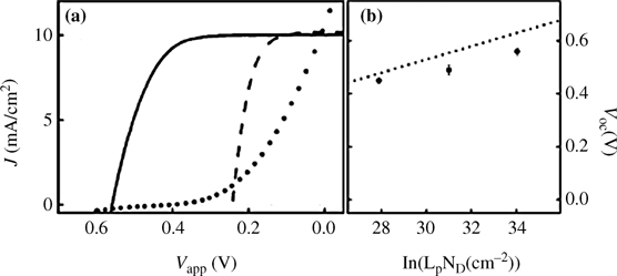
FIGURE 12.24 (a) J–E behavior for H–Si(111) (dotted line) and CH3–Si(111) (solid line) in contact with sintered Au nanoparticles and H–Si(111) (dashed line) in contact with evaporated Au (b) Measured Voc values versus ln(LpND) for n-Si/Au devices made with CH3-terminated n-Si (111) and sintered Au NP films. The dotted line represents the bulk-recombination-limited Voc. Figures reproduced from Ref. 158 by permission of the American Chemical Society, © 2008.
12.4.1 Tethered Redox Centers
Electrochemical oxidation of silicon occurs when deleterious oxidation events occur competitively with the productive charge-transfer event. Facilitation of productive charge transfer can prevent passivation of the Si. This behavior has been demonstrated by the tethering of a redox-active center to n-type silicon. A ferrocene-derivatized silane was attached to n-Si(111), and the photoanodic performance was evaluated [159–161]. It was shown that charge transfer to Ru(NH3)62+/3+, Fe(CN)64–/3–, and I–/I3– could be facilitated by the bound ferrocene. Current-voltage cycling of the bound ferrocene produced nearly identical data for 1000 cycles, whereas bare photoanodes could not produce even one reproducible voltage sweep. Furthermore, functionalized electrodes were stable, to within 10% of the original photocurrent, for >5 h of continuous illumination with a turnover number of >10–5. The photocurrent at bare electrodes decayed by >90% within 5 min of operation under anodic conditions.
In addition to bound individual redox-active species, stability enhancements have been demonstrated with polymeric methyl viologen-based derivatives [162]. When illuminated in solution with a redox reagent, Fe(CN)64–, the poly(methyl viologen)-coated n-Si electrodes exhibit enhanced stability. Coatings with a non-redox-active, but charged, backbone, derived from (CH3O)3Si(CH2)3N+(CH3)3, also exhibited enhanced stability presumably because electrostatic binding interactions drew solution redox ions close to the electrode. In this fashion, direct charge transfer to the redox species was not inhibited, but a physical barrier blocked molecules that could undergo deleterious oxidation reactions with the underlying n-Si. In all cases, the photocurrent stability enhancement was a balance between the physical barrier and charge-transport limitations (Fig. 12.25).
12.4.2 Conductive Polymer Coatings
The previous section discussed the use of long-chain alkanes to form a physical barrier to chemical oxidants. Although this approach could be extrapolated to long chains, such long chains introduce a detrimental effect on the photoelectrode efficiency, in the form of a series resistance, because thicker barriers must be conductive in order to pass charge across the interface.
The deposition of polypyrrole (PPy) on small bandgap semiconductors such as n-GaAs, n-CdTe, n-CdSe, and n-CdS has resulted in improved stability under both cyclic voltammetric and continuous illumination photoanodic conditions [163,164]. Specifically, polypyrrole-coated GaAs has been shown to be stable for >100 h in methanol (Fig. 12.26), whereas bare GaAs is stable under the same conditions for only a few minutes. Peeling of the polymer was a problem for these systems, and eventual oxidation was attributed to deleterious reactions at sites of peeling. The peeling was worse in water; PPy-coated photoanodes were stable only for 10–20 min in water. Within that 10–20 min, an efficiency of 10.5% was achieved for the aqueous oxidation of Fe(CN)3-/4- under 170mW/cm2 illumination.
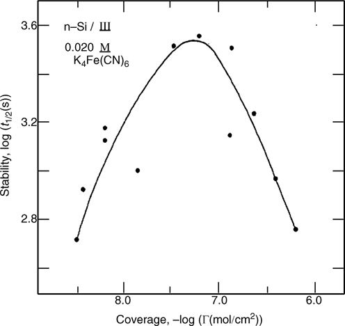
FIGURE 12.25 Photoanodic stability of n-Si/electroactive polymer/0.020 M Fe(CN)64– (aq) junctions at constant light intensity (1.0mW/cm2 at 632.8 nm) as a function of polymer coverage in mol/cm2 of electroactive monomeric units. Figure reproduced from Ref. 162 by permission of the American Chemical Society, © 1984.
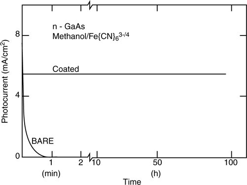
FIGURE 12.26 JSC versus time characteristics showing the photoanodic stability of bare and polypyrrole-coated n-GaAs electrodes in contact with methanolic 0.1 M Et4NBF4/0.2M Fe(CN)63-/4- solution. Figure taken from Ref. 164.
In contact with various redox couples, PPy was also demonstrated to increase the stability of n-Si photoanodes that were coated with 5 Å of vacuum-evaporated Pt [165,166]. The initial photocurrent density was approximately 7% higher for n-Si/Pt photoanodes compared to n-Si/PPy/Pt, but the performance of the surfaces that did not have a PPy coating decayed within 4 h [165]. PPy-coated n-Si/Pt was continuously operated in an aqueous I–/I3– cell for over 6 days, when the experiment was arbitrarily ended (Fig. 12.27). Without the Pt, electrodes with PPy were stable for only a few minutes, and bare n-Si was stable for less than 1 min in this medium. The effects of metal deposition on stability are further discussed below. The VoC observed for n-Si/Pt/PPy was 0.425 V, and varied by less than 100 mV for a change in redox potential of 1.25 eV. In contact with an acidic aqueous solution of FeSO4/FeNH4(SO4)2, the n-Si/PPy with no Pt was stable for 120 h, with a decline of ~30% in photovoltage [167]. The stabilization effect has also been observed for PPy electrodeposited on amorphous, hydrogenated silicon [168].
Organic monolayers have been used to enhance the adherence of the PPy films to semiconductor surfaces. Electropolymerization of pyrrole was initiated at a pyrrole-functionalized silane self-assembled monolayer [169]. Films deposited onto this surface showed enhanced stability in contact with an aqueous FeCl3/FeCl2/1 M HCl solution, and showed stable photocurrent densities of 7.8 mA/cm2 for >25 h. In contrast, films that were not covalently attached to the electrode surface showed a drop in photocurrent density from 6.5 to 1.8 mA/cm2 in less than 18 h. The increase in stability was attributed to a drastic decrease in the peeling of the films (Fig. 12.28). This idea has been applied more recently to oxide-free semiconductor surfaces in which H-terminated Si surfaces were functionalized with an alkyllithium chain bearing a pyrrole. Polymer films electrodeposited at the pyrrole-functionalized surface were smoother than polymer films electrodeposited at a Si–H surface, as observed using AFM, and the diode quality factor dropped from 2.3 (at noncovalently linked Si/PPy junctions) to 1.5 (Fig. 12.29). The decrease in ideality factor is consistent with an increase in sites of contact between the Si and PPy [170]. Polythiophene derivatives have been electropolymerized at surfaces that were functionalized with a di(2-thienyl)carbinoyl obtained from the reaction of thienyl lithium with an acid-terminated organic monolayer that was formed via hydrosilylation [170]. Surface states that were suggested to dominate interfacial energetics were observed by capacitance versus voltage methods. The maximum VOC observed for the n-Si/polythiophene system was 390 mV. It was suggested that the low VOC was attributable to film inhomogeneities, under which the current preferentially flowed through regions of low barrier height. Alternatively, adhesion and stability were improved by first depositing a Au film [171].
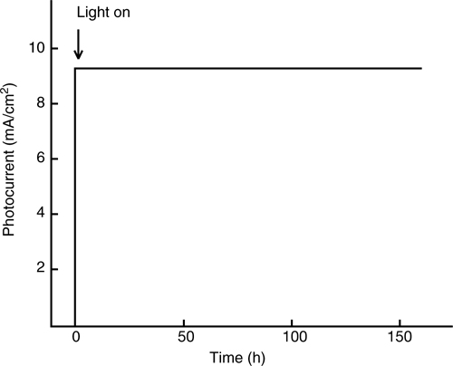
FIGURE 12.27 JSC versus time characteristics showing the photoanodic stability for n-Si/Pt/polypyrrole electrodes in contact with 0.1 M KI, 0.01 M I2, and 0.1 M KCl(aq), and illuminated at 75 mW/cm2 by a tungsten halogen lamp. Polypyrrole was 250 monolayers thick. Taken from Ref. 165.
In addition to the demonstration of enhanced photoanodic stability, conductive polymers can make highly rectifying and ohmic, non-Fermi-level-pinned contacts to both n- and p-Si (Fig. 12.30) [173,174]. Ring-opening metathesis polymerization (ROMP) was used to make well-defined Si/polyacetylene (PA) junctions. PA can be doped with either K metal or I2 to give n- and p-type PA, respectively. The exchange current density, J0, was 6×10⁻⁷ and 2.4×10⁻⁸ A/cm2 at p-Si/(CHK0.06)x and n-Si/(CHI0.17)x, respectively, whereas at most metals J0 is typically on the order of 10–3 A/cm2. Higher rectification was thus observed at Si/PA junctions than at metal/Si junctions. n-Si/poly(CH3)3Si-COT contacts exhibited VOC of up to 0.64 V [174].
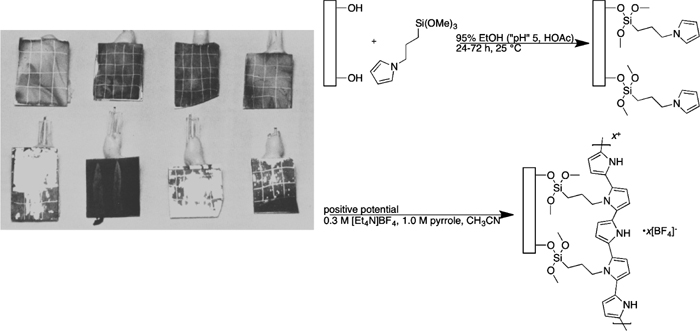
FIGURE 12.28 Comparisons of the peel-off test of polypyrrole-coated n-Si electrodes. The top four electrodes were first modified with a pyrrole-functionalized silane (modification scheme shown at right), while polypyrrole was deposited on bare Si for the bottom four electrodes. Figures reproduced from Ref. 169 by permission of the American Chemical Society, © 1982.
12.4.3 Metal Films
12.4.3.1 Stability Enhancement
Improvement in the stability of Si and other small bandgap semiconductors has been achieved by facilitation of charge transfer through the deposition of metal overlayers onto the electrode surface [175–177]. Accordingly, anodic and photoanodic stability of n-GaP, n-Si, p-GaP, and p-Si has been achieved by use of evaporated Au, Pd, or Ag films [175,176]. The devices exhibited very low VOC and no dependence of VOC on the redox potential of the solution, although this could be avoided by depositing thinner metal layers without loss of the added stabilization [175,177].
A combination of metallic and nonmetallic overlayers, such as Pt on a thin SiO2, inhibits further electronic passivation [177,178]. At 10 Å deposition, the junction electrical properties were still determined by the contacting solution; however, at 20 or 40 Å of film thickness, the interfacial energetics were dominated by the Si/Pt junction.
12.4.3.2 Deposition on Organic Monolayers
As discussed earlier, evaporation of metal, even on Si–C terminated silicon, leads to silicide formation and Fermi level pinning at Si/metal junctions [155]. Evaporated metal penetrates –CH3 terminated monolayers on Si [179–182]. In some cases, increasing the physical barrier to metal penetration, by increasing the monolayer chain length, has no effect [182]. Soft contacting techniques such as sintered Au nanoparticles [158], electrodeposition of Cd and Pb [130], LOFO [183], and polymer-assisted lift-off (PALO) [184] show some promise; however, recently, utilization of monolayer functionality for improved Si/metal junctions has been explored.
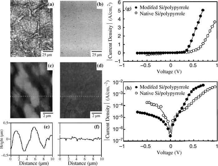
FIGURE 12.29 Optical micrographs (a, b) and AFM images (c, d) for polypyrrole films electrodeposited on H–Si(111) (a, c) and 5-(N-pyrrolyl)pentyl–Si(111) (b, d). Cross-sectional images (e, f) are taken from the dotted lines denoted in the AFM images (c, d). J–E (g) and log (J)–E (h) behavior of polypyrrole/n-Si(111) junctions formed at H–Si(111) (open symbols) and 5-(N-pyrrolyl)pentyl–Si(111) (filled symbols) surfaces. Reproduced from Ref. 172 by permission of the American Institute of Physics, © 1999.
The morphology of evaporated films was observed to change with changes in the functionality of the monolayer [185,186]. Dithiodiacid and dithiodisilane reagents have been used to functionalize oxidized Al and Si surfaces, respectively. Evaporated Au films on treated surfaces were observed to be continuous at lower thicknesses than on bare surfaces, as determined via film resistivity measurements and TEM images. This behavior was attributed to the interaction of incoming Au atoms with the terminating thiol groups [185]. E-beam evaporated Au films on oxidized Si surfaces treated with (3-mercaptopropyl)trimethoxysilane exhibited a surface roughness factor of ~2Å over 1 mm2 area [186].
The interaction of terminal functionality with incoming metal atoms affords an opportunity to prevent metal penetration to the Si surface during the deposition step. ToF-SIMS has been a major tool in determination of metal penetration through monolayers versus accumulation at the monolayer-vacuum interface. ToF-SIMS data on Au evaporation onto –CH3 terminated monolayers on Au showed no change in the positive ion spectrum, even after deposition of 50 EL (equivalent layers or metal atoms/SAM molecule) of Au atoms (Fig. 12.31) [179]. In addition, very little change was observed in the negative ion spectra, and no new ion peaks were observed. This behavior suggests that the monolayers “float” on top of the deposited Au.
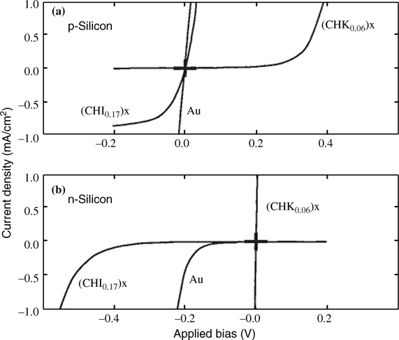
FIGURE 12.30 J–E behavior at Si/p-PA, Si/n-PA, and Si/Au junctions formed by ROMP of cyclooctatetraene at Si surfaces. p-type PA forms nearly ohmic contacts with p-Si (a) and highly rectifying contacts with n-Si (b). Likewise, n-type PA forms highly rectifying contacts with p-Si (a) and ohmic contacts with n-Si (b). Evaporated Au forms ohmic contacts with p-Si (a) and weakly rectifying contacts with n-Si (b). Reproduced from Ref. 173.
An interaction between evaporation-deposited Cu atoms and a monolayer organic functional end group (OFG), –C(O)OH, was observed by XPS [187]. High-resolution XP spectra of the O 1s region showed peaks at 532.8 and 531.9 eV, representing the C(O)OH and C(O)OH peaks, respectively. After deposition of 1 nm of Cu, the region showed peaks at 531.6 and 530.8 eV, representing the C(O)OCu and C(O)OCu, respectively.
Interactions between metal atoms and OFGs are specific. As the OFG identity is changed, the ratio of vacuum-evaporated Au monolayer penetration and deposition at the monolayer–vacuum interface also changes [179]. ToF-SIMS, AFM, and CPAFM have been used to analyze the extent to which monolayer penetration occurred in each system of interest. AFM images revealed that in the case of metal penetration, the structure of the Au(111) substrate was still clearly visible. If, however, the deposition occurred above the monolayer, mushroom-like Au particles were observable, or a more disordered film was seen. CPAFM was used to reveal shorts, indicative of Au filaments spanning the monolayer with some deposition at the monolayer/vacuum interface. Less Au penetrated to the substrate when the OFG was changed from –CH3 to –C(O)OCH3 to C(O)OH to C(O)O–K+ (Fig. 12.32). This behavior is consistent with the expectations for the different physical barriers produced by the interactions between the metals and the different OFGs.
FIGURE 12.31 Positive ion ToF-SIMS spectra of CH3-terminated films with Au dose for 0, 13, and 50 equivalent layers of Au. The absence of any change in the spectra suggests the Au is penetrating the CH3-terminated monolayers. Reproduced from Ref. 179 by permission of the American Chemical Society, © 2006.
Grazing incidence FTIR (GI-FTIR) has been used to observe the interactions between metal atoms and OFGs. Upon deposition of Au and Al onto thiol-terminated SAMs, the monolayer peaks decreased in intensity, but neither a peak broadening nor a peak shift was observed, as would be expected upon disruption of the monolayer [188]. Deposition on the arylterminated monolayers resulted in a peak broadening and a peak shift, but without much change in peak intensity. This behavior indicated penetration of metal atoms through the monolayer. Consistently, deposition of Ti destroyed all of the monolayers tested.
Al was observed to react with –OH terminated monolayers to completion, rather than penetrating to the monolayer/substrate interface [189]. A dielectric Al layer was formed at low Al coverages. XP spectra at various deposition thicknesses showed a shift of the O binding energy, from 533.4 eV to a broadened peak at 532.6 eV, suggesting formation of an Al–O species. In addition, at low deposition thicknesses, the Al peak was very broad, at 75.2 binding eV (BeV). At high Al thickness, a metallic peak was observed to grow in at 72.9 BeV, with retention of the nonmetallic Al–O species. IR spectra before and after deposition also showed changes in the C–O stretching frequency upon conversion from C–OH to C–OAl, and a peak assignable to Al–O species, at 850 cm–1, appeared. By comparison, deposition on –OCH3 terminated monolayers showed penetration of the monolayer via observation of Al–S via XPS and ToF-SIMS. Interaction of different noble metals with the –OCH3 terminated monolayer was explored using ToF-SIMS, infrared reflection spectroscopy, and XPS [180]. Al penetrated the monolayer until the monolayer substrate interface was 1:1 Al/Au. In contrast, Cu and Ag continuously partitioned deposition through, and on top of, the monolayer. Au only deposited through the monolayer, and the monolayer was observed to float on top.
FIGURE 12.32 Schematic illustration of Au behaviors on different self-assembled monolayers (SAMs). (a) Continuous, uniform penetration leading to smooth buried underlayers is seen for Au on the CH3 and CO2CH3 SAMs; (b) penetration of Au to form conducting filaments with connected overlayer clusters, seen for Au on the CO2H SAM; (c) high interaction of incoming Au with monolayer OFGs, as seen for Au on the K-modified CO2CH3 and CO2H films, leads to nucleation of overlayer clusters with initial scattered penetration into the self-assembled monolayer and, at higher coverages, penetration leading to formation of scattered conducting filaments connected to overlayer clusters in mushroom-like overlayer deposits and contiguous overlayer islands. Figure reproduced from Ref. 179 by permission of the American Chemical Society, © 2006.
The J–V characteristics provide an additional indicator of the extent of monolayer penetration [179,182]. For example, Au has been evaporated onto –CH3 and –SH terminated monolayers formed by hydrosilylation of Si [179]. J–V and capacitance–voltage measurements on the Au/monolayer/Si junctions showed similar effective barrier heights and built-in potentials regardless of the nature of the OFG. Nanoscale electrical measurements via ballistic electron emission microscopy (BEEM) closely matched the macroscopic measurements, and threshold voltages were approximately the same across all of the samples, including evaporated films on H-terminated silicon. The current decreased by over 80% for functionalized samples, with a marked difference between –CH3 and –SH terminated monolayers because of the difference in metal penetration (Fig. 12.33). TEM showed much higher Au penetration for the –CH3 OFGs; however, Au penetration of the monolayer was observed for all surface treatments (Fig. 12.33).
Terminal functionality of monolayers has been utilized to facilitate other metal deposition techniques, such as transfer printing (TP) and nanotransfer printing (nTP) [190–192]. These techniques utilize the interaction between a metal, for example Au, and the terminal end of an organic monolayer; 1,8-octanedithiol on GaAs served as an early example to demonstrate transfer of an evaporated metal film [190]. By introduction of functionality to the organic monolayer, direct evaporation is avoided. Instead, the metal films are evaporated onto a treated PDMS stamp that has poor adhesion to the metal, and the films are then transferred to a surface terminated with strongly interacting functional groups, to make the desired metal/organic monolayer/semiconductor structures. The use of TP to contact Si with Au yields a pure metal–insulator–semiconductor structure [193]. The tunneling through the monolayer was shown to be purely temperature independent, in contrast to the behavior of Au evaporated on –SH monolayers. This method also readily forms nanoscale metal patterns with the master pattern being formed in the PDMS stamp, thus avoiding repetitive, costly lithography steps. SAMs of a thiol-terminated silane, (CH3)3Si(CH2)3SH, were formed on oxidized Si for the transfer of Au films to Si surfaces (Fig. 12.34) [191]. nTP can make Cu contacts as well, with one additional processing step [192].
The stamp approach to contact patterning can also be used to pattern the initial monolayer [194]. In this method, the stamp catalyzes hydrosilylation at the points of contact. Gold nanoparticles then deposited preferentially on the patterned monolayers. Pd nanoparticle–OFG interactions have been used to seed electroless Ni deposition; however, the resulting junction properties very closely resembled those of evaporated Ni [195].
FIGURE 12.33 Cross-sectional TEM images of evaporated Au/organic monolayer/Si(111) interface. (a, c) Au/C10H13–Si(111) at low (bright field) and high magnification (phase contrast images); (b, d) Au/HSC11H22–Si(111) at low and high magnification. (e) Corresponding averaged BEEM spectra for (a), (b), and Au/H–Si(111) and Au/CH3C(O)SC11H22–Si(111) junctions. Figures reproduced from Ref. 182 by permission of the American Chemical Society, © 2008.
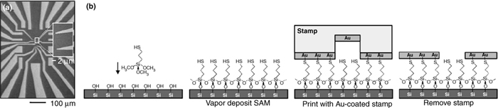
FIGURE 12.34 (a) Optical micrograph of Au pattern formed by nanoscale transfer printing, (b) Scheme for creating nanoscale transfer printed Au pads on Si surfaces. Figure reproduced from Ref. 191 by permission of the American Chemical Society, © 2002.
Physical vapor deposition of metal on patterned monolayers consisting of more than one OFG has utilized the differential extent of monolayer penetration to pattern contacts [181]. In this method, the metal atoms deposit at the monolayer-substrate interface over a portion of the monolayer, and on top of the monolayer over the rest of the surface.
12.4.4 Semiconducting and Nonmetallic Coatings
12.4.4.1 Stability Enhancement
Nonmetallic coatings have been used frequently to stabilize Si under anodic or photoanodic conditions. ITO [196,197], other doped SnO2 films [198], boron phosphide [199], thallium(III) oxide [200], TiO2 [201], Fe2O3 [202], and even silicides [203] have been used. These techniques have yielded high-efficiency devices; for example, the n-Si/thallium(III) oxide/ferricyanide electrochemical cell achieved 11.0% efficiency under natural light. An early problem was deposition of thick overlayers. For example, deposition of TiO2 onto n-Si showed only the photoelectrochemical properties of the TiO2 [201]. Thus, methods such as ALD that can deposit thinner semiconducting films are desirable.
12.4.4.2 Deposition on Si by ALD
In addition to thin protective layers, ALD on Si is of interest for transistors. The fundamental limitations on the use of SiO2 as a dielectric in transistors cause problems for the future scale of electronics [73]. The thickness required, low dielectric constant, k, and high leakage currents make SiO2 not well suited for low-power applications or for the next stages of miniaturization of electronics. As low interfacial trap state densities are crucial, it would be difficult to create a more ideal interface than that of a well-prepared Si/SiO2 interface, which has a typical midgap interface state density of 2×10¹⁰ states/cm2. Most interfaces fabricated using ALD have between one and two orders of magnitude higher interfacial trap state density. In addition, these interfaces exhibit substantial flat-band voltage shifts, in excess of 300 mV. For high-quality devices, no silicide or metal oxide phases should be at or near the channel interface, because silicide and most M–Si bonding will lead to poor leakage currents and low electron channel mobilities.
ALD is thus an attractive method to circumvent these difficulties by controlling the interfacial chemistry. Unfortunately, due to a lack of reactivity, ALD requires extreme conditions to yield film growth on Si–H [204]. ALD generally utilizes very high reactivity, but self-limiting, reactions for controlled material preparation. The Si–H surface simply does not have the inherent required reactivity. Long initial exposure times, of 3600 s, with H2O, or an initial exposure to a metal precursor, Al(CH3)3 for example, are thus necessary to initiate uniform growth on Si [204]. Si oxidation was observed to occur during this time, due to impurity M–OR species in the metal feed [205]. After metal binding, oxidation by H2O was catalyzed. Oxidation during growth was more pronounced on the Si(100) face. One TMA exposure catalyzed the growth of 1.2 Å SiOx.
Just as the evaporation of metal onto end-functionalized organic monolayers affected the extent of penetration to the substrate and the final metal film morphology, a similar effect occurs in ALD [206,207]. ALD of Ti[N(CH3)2]4 at SAMs of alkyltrichlorosilanes with –OH, –NH2, and –CH3 OFGs was studied as a step toward understanding the deposition of titanium nitride on organic monolayers [206]. The reaction proceeded at every temperature tested. Angle-resolved XPS was used to observe whether Ti deposition occurred at the SiO2/SAM or SAM/vacuum interface (Fig. 12.35). Deposition on –CH3 terminated monolayers penetrated to the SAM/SiO2 interface, and partitioned to both interfaces at –OH functionalized SAMs. The –NH2 terminated SAM showed reactivity solely at the SAM/vacuum interface. In addition, deposition rates at –CH3 terminated SAMs were severely attenuated, and islanding was observed using AFM [111]. Growth at –OH and –NH2 surfaces was less attenuated, but growth was not uniform until thicker depositions were performed.
In situ and ex situ IR and XPS have been used to observe metal interactions with OFGs, during ALD of metallic Cu using [Cu(sBu-amd)]2 as a precursor [208]. IR data showed that a carboxylic acid-terminated monolayer interacts with Cu atoms in a bidentate fashion without the formation of a SiOx layer (Fig. 12.36). This work serves as a demonstration that high-quality metallic contacts can be made to Si using ALD. Unlike deposition on H-terminated Si surfaces, Al2O3 can be deposited at –COOH terminated monolayers on Si, without the formation of oxide [209]. TIR observation of Al2O3 growth showed formation of a high-quality film. The absence of any shifts or changes in the C–H region of the IR showed no disruption of the monolayer. Stringent conditions in monolayer preparation, and interaction of ALD reagents with the –COOH rather than penetration to the SAM/Si interface, thus prevented formation of SiOx species. Characteristic SiOx vibrational modes only appeared upon heating to >400° C.
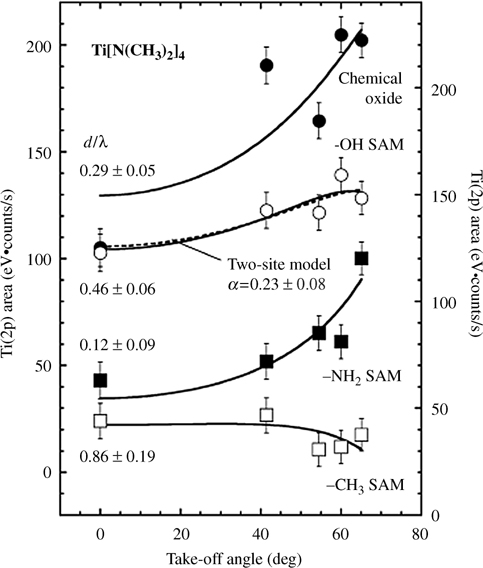
FIGURE 12.35 Angle-dependent integrated Ti 2p intensity for the adsorption of ALD precursor Ti[N(CH3)2]4 on Si chemical oxide (filled circles, left axis), –OH terminated SAM (open circles, left axis), –NH2 terminated SAM (filled squares, right axis), and –CH3 terminated SAM (open squares, right axis). The curves represent a fit to a model that assumes that the Ti is uniformly distributed at a depth d from the surface, and the inelastic mean free path of the Ti 2p photoelectrons is λ. The value d/λ is given for each case. Reproduced from Ref. 206 by permission of the American Chemical Society, © 2005.
12.5 CONCLUSIONS
Si–C termination renders Si surfaces much more stable to a larger range of working conditions than is observed for H- or halogen-terminated silicon surfaces. The increased stability stems from the kinetic stability of Si–C bonds and from the physical barrier imposed by a well-ordered organic film. Increased stability does not necessarily have to produce a loss of beneficial electronic properties. Beyond the stability imparted by the Si–C group, functional organic monolayers have great utility in the fabrication of advanced device structures. Classic problems with Si, including oxidation in air and Fermi level pinning in contact with most metals, can be overcome by the clever use of organic monolayers. Global device issues such as high-cost patterning can be avoided by the use of cheaply patterned monolayers. A thorough understanding of the surface chemistry of Si thus enables the formation of well-defined, electronically preserved interfaces and, ultimately, more efficient devices in a variety of optoelectronic applications.
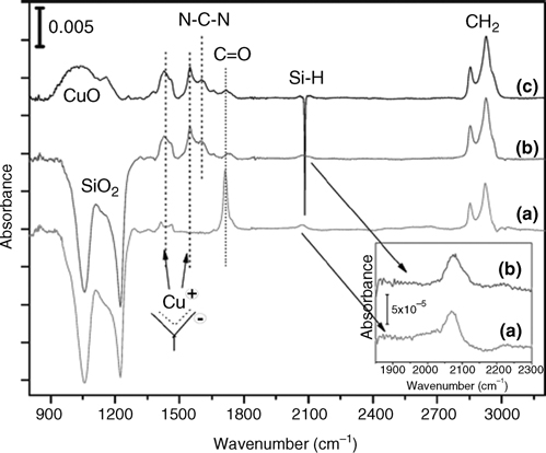
FIGURE 12.36 Absorption spectra of ALD deposition of Cu metal at a COOH-terminated SAM on Si. (a) COOH-terminated SAM referenced to the Si native oxide; (b, c) COOH- terminated SAM with 20 Cu ALD cycles referenced to the native oxide and H-terminated surfaces, respectively. Figure reproduced from Ref. 208 by permission of the American Chemical Society, © 2009.
REFERENCES
1. Yablonovitch, E.; Gmitter, T. J. Solid State Electron. 1992, 35, 261–267.
2. Yablonovitch, E.; Allara, D. L.; Chang, C. C.; Gmitter, T.; Bright, T. B. Phys. Rev. Lett. 1986, 57, 249–253.
3. Heller, A. Solar Energy 1982, 29, 153–162.
4. Grunthaner, F. J.; Grunthaner, P. J. Mater. Sci. Rep. 1986, 1, 65–160.
5. Grundner, M.; Jacob, H. Appl. Phys. A 1986, 39, 73–82.
6. Rappich, J.; Lewerenz, H. J. J. Electrochem. Soc. 1995, 142, 1233–1237.
7. Dittrich, T.; Rauscher, S.; Bitzer, T.; Aggour, M.; Flietner, H.; Lewerenz, H. J. J. Electrochem. Soc. 1995, 142, 2411–2413.
8. Rappich, J.; Jungblut, H.; Aggour, M.; Lewerenz, H. J. J. Electrochem. Soc. 1994, 141, L99-L102.
9. Bitzer, T.; Gruyters, M.; Lewerenz, H. J.; Jacobi, K. Appl. Phys. Lett. 1993, 63, 397–399.
10. Ibach, H.; Rowe, J. E. Surf. Sci. 1974, 43, 481–492.
11. Mayer, T. M.; Lampe, F. W. J. Phys. Chem. 1974, 78, 2429–2433.
12. Burrows, V. A.; Chabal, Y. J.; Higashi, G. S.; Raghavachari, K.; Christman, S. B. Appl. Phys. Lett. 1988, 53, 998–1000.
13. Chabal, Y. J.; Higashi, G. S.; Raghavachari, K.; Burrows, V. A. J. Vac. Sci. Technol. A 1989, 7, 2104–2109.
14. Clark, I. T.; Aldinger, B. S.; Gupta, A.; Hines, M. A. J. Phys. Chem. C 2010, 114, 423–428.
15. Higashi, G. S.; Becker, R. S.; Chabal, Y. J.; Becker, A. J. Appl. Phys. Lett. 1991, 58, 1656–1658.
16. Higashi, G. S.; Chabal, Y. J.; Trucks, G. W.; Raghavachari, K. Appl. Phys. Lett. 1990, 56, 656–658.
17. Hines, M. A. Annu. Rev. Phys. Chem. 2003, 54, 29–56.
18. Wade, C. P.; Chidsey, C. E. D. Appl. Phys. Lett. 1997, 71, 1679–1681.
19. Cicero, R. L.; Linford, M. R.; Chidsey, C. E. D. Langmuir 2000, 16, 5688–5695.
20. Jakob, P.; Chabal, Y. J.; Raghavachari, K. Chem. Phys. Lett. 1991, 187, 325–333.
21. Jakob, P.; Dumas, P.; Chabal, Y. J. Appl. Phys. Lett. 1991, 59, 2968–2970.
22. Cowley, A. M.; Sze, S. M. J. Appl. Phys. 1965, 36, 3212–3220.
23. Linnros, J. J. Appl. Phys. 1998, 84, 275–283.
24. Angermann, H.; Kliefoth, K.; Flietner, H. Appl. Surf. Sci. 1996, 104, 107–112.
25. Wittmer, M.; Freeouf, J. L. Phys. Lett. A 1993, 173, 190–194.
26. Wittmer, M.; Freeouf, J. L. Phys. Rev. Lett. 1992, 69, 2701–2704.
27. Gstrein, F.; Michalak, D. J.; Royea, W. J.; Lewis, N. S. J. Phys. Chem. B 2002, 106, 2950–2961.
28. Michalak, D. J.; Amy, S. R.; Esteve, A.; Chabal, Y. J. J. Phys. Chem. C 2008, 112, 11907–11919.
29. Michalak, D. J.; Gstrein, F.; Lewis, N. S. J. Phys. Chem. C 2008, 112, 5911–5921.
30. Michalak, D. J.; Gstrein, F.; Lewis, N. S. J. Phys. Chem. C 2007, 111, 16516–16532.
31. Ciampi, S.; Harper, J. B.; Gooding, J. J. Chem. Soc. Rev. 2010, 39, 2158–2183.
32. Lehmann, V. Electrochemistry of Silicon. Wiley-VCH, Weinheim, 2002.
33. Tuck, B. J. Mater. Sci. 1975, 10, 321–339.
34. Henderson, R. C. J. Electrochem. Soc. 1972, 119, 772.
35. Kern, W.; Puotinen, D. A. RCA Rev. 1970, 31, 187–206.
36. Kern, W. J. Electrochem. Soc. 1990, 137, 1887–1892.
37. Kern, W. RCA Rev. 1978, 39, 278–308.
38. Sato, K.; Shikida, M.; Matsushima, Y.; Yamashiro, T.; Asaumi, K.; Iriye, Y.; Yamamoto, M. Sens. Actuators A 1998, 64, 87–93.
39. Mende, G.; Finster, J.; Flamm, D.; Schulze, D. Surf. Sci. 1983, 128, 169–175.
40. Niwano, M.; Kageyama, J.; Kurita, K.; Kinashi, K.; Takahashi, I.; Miyamoto, N. J. Appl. Phys. 1994, 76, 2157–2163.
41. Zhang, X.; Garfunkel, E.; Chabal, Y. J.; Christman, S. B.; Chaban, E. E. Appl. Phys. Lett. 2001, 79, 4051–4053.
42. Yasaka, T.; Takakura, M.; Sawara, K.; Uenaga, S.; Yasutake, H.; Miyazaki, S.; Hirose, M. IEICE Trans. Electron. 1992, E75C, 764–769.
43. Cleland, G.; Horrocks, B. R.; Houlton, A. J. Chem. Soc., Faraday Trans. 1995, 91, 4001–4003.
44. Yu, H.-Z.; Morin, S.; Wayner, D. D. M.; Allongue, P.; Henry de Villeneuve, C. J. Phys. Chem. B 2000, 104, 11157–11161.
45. Boukherroub, R.; Morin, S.; Sharpe, P.; Wayner, D. D. M.; Allongue, P. Langmuir 2000, 16, 7429–7434.
46. Michalak, D. J.; Rivillon, S.; Chabal, Y. J.; Esteve, A.; Lewis, N. S. J. Phys. Chem. B 2006, 110, 20426–20434.
47. Warntjes, M.; Vieillard, C.; Ozanam, F.; Chazalviel, J. N. J. Electrochem. Soc. 1995, 142, 4138–4142.
48. Bateman, J. E.; Eagling, R. D.; Horrocks, B. R.; Houlton, A. J. Phys. Chem. B 2000, 104, 5557–5565.
49. Hory, M. A.; Herino, R.; Ligeon, M.; Muller, F.; Gaspard, F.; Mihalcescu, I.; Vial, J. C. Thin Solid Films 1995, 255, 200–203.
50. Hacker, C. A.; Anderson, K. A.; Richter, L. J.; Richter, C. A. Langmuir 2004, 21, 882–889.
51. Bateman, J. E.; Horrocks, B. R.; Houlton, A. J. Chem. Soc., Faraday Trans. 1997, 93, 2427–2431.
52. Chazalviel, J. N. J. Electroanal. Chem. 1987, 233, 37–48.
53. Sze, S. M. The Physics of Semiconductor Devices, 2nd ed. Wiley, New York, 1981.
54. Kampen, T. U.; Monch, W. Surf. Sci. 1995, 331, 490–495.
55. Kampen, T. U.; Schmitsdorf, R. F.; Monch, W. Appl. Phys. A 1995, 60, 391–394.
56. Kurtin, S.; McGill, T. C.; Mead, C. A. Phys. Rev. Lett. 1969, 22, 1433–1436.
57. Severin, P. J.; Poodt, G. J. J. Electrochem. Soc. 1972, 119, 1384.
58. Schaffer, P. S.; Lally, T. R. Solid State Technol. 1983, 26, 229–233.
59. Maldonado, S.; Plass, K. E.; Knapp, D.; Lewis, N. S. J. Phys. Chem. C 2007, 111, 17690–17699.
60. Villarrubia, J. S.; Boland, J. J. Phys. Rev. Lett. 1989, 63, 306–309.
61. Aldao, C. M.; Weaver, J. H. Prog. Surf. Sci. 2001, 68, 189–230.
62. Horanyi, T. S.; Pavelka, T.; Tutto, P. Appl. Surf. Sci. 1993, 63, 306–311.
63. M'Saad, H.; Michel, J.; Lappe, J. J.; Kimerling, L. C. J. Electron. Mater. 1994, 23, 487–491.
64. Stephens, A. W.; Green, M. A. Solar Energy Mater. Solar Cells 1997, 45, 255–265.
65. Hamers, R. J. Surf. Sci. 2006, 600, 3361–3362.
66. He, J.; Patitsas, S. N.; Preston, K. F.; Wolkow, R. A.; Wayner, D. D. M. Chem. Phys. Lett. 1998, 286, 508–514.
67. Bansal, A.; Li, X. L.; Lauermann, I.; Lewis, N. S.; Yi, S. I.; Weinberg, W. H. J. Am. Chem. Soc. 1996, 118, 7225–7226.
68. Cai, W.; Lin, Z.; Strother, T.; Smith, L. M.; Hamers, R. J. J. Phys. Chem. B 2002, 106, 2656–2664.
69. Zhu, X.-Y.; Boiadjiev, V.; Mulder, J. A.; Hsung, R. P.; Major, R. C. Langmuir 2000, 16, 6766–6772.
70. Bergerson, W. F.; Mulder, J. A.; Hsung, R. P.; Zhu, X.-Y. J. Am. Chem. Soc. 1999, 121, 454–455.
71. Klaus, J. W.; Sneh, O.; George, S. M. Science 1997, 278, 1934–1937.
72. Buriak, J. M. Chem. Rev. 2002, 102, 1271.
73. Wilk, G. D.; Wallace, R. M.; Anthony, J. M. J. Appl. Phys. 2001, 89, 5243.
74. Guha, S.; Cartier, E.; Gribelyuk, M. A.; Bojarczuk, N. A.; Copel, M. C. Appl. Phys. Lett. 2000, 77, 2710.
75. Edge, L. F.; Schlom, D. G.; Brewer, R. T.; Chabal, Y. J.; Williams, J. R.; Chambers, S. A.; Hinkle, C.; Lucovsky, G.; Yang, Y.; Stemmer, S.; Copel, M. C.; Hollander, B.; Schubert, J. Appl. Phys. Lett. 2004, 84, 4629–4631.
76. Terry, J.; Mo, R.; Wigren, C.; Cao, R.; Mount, G.; Pianetta, P.; Linford, M. R.; Chidsey, C. E. D. Nucl. Instrum. Methods Phys. Res. B 1997, 133, 94.
77. Rivillon, S.; Chabal, Y. J.; Webb, L. J.; Michalak, D. J.; Lewis, N. S.; Halls, M. D.; Raghavachari, K. J. Vac. Sci. Technol. A 2005, 23, 1100–1106.
78. Florio, J. V.; Robertson, W. D. Surface Science 1969, 18, 398–427.
79. Li, Z.; Kamins, T. I.; Li, X.; Williams, R. S. Surf. Sci. 2004, 554, L81–L86.
80. Rivillon, S.; Amy, F.; Chabal, Y. J.; Frank, M. M. Appl. Phys. Lett. 2004, 85, 2583–2585.
81. Eves, B. J.; Lopinski, G. P. Surf. Sci. 2005, 579, L89–L96.
82. Bansal, A.; Li, X. L.; Yi, S. I.; Weinberg, W. H.; Lewis, N. S. J. Phys. Chem. B 2001, 105, 10266–10277.
83. Cao, P.; Yu, H.; Heath, J. R. J. Phys. Chem. B 2006, 110, 23615–23618.
84. Webb, L. J.; Lewis, N. S. J. Phys. Chem. B 2003, 107, 5404–5412.
85. Webb, L. J.; Nemanick, E. J.; Biteen, J. S.; Knapp, D. W.; Michalak, D. J.; Traub, M. C.; Chan, A. S. Y.; Brunschwig, B. S.; Lewis, N. S. J. Phys. Chem. B 2005, 109, 3930–3937.
86. Yu, H. B.; Webb, L. J.; Solares, S. D.; Cao, P. G.; Goddard, W. A.; Heath, J. R.; Lewis, N. S. J. Phys. Chem. B 2006, 110, 23898–23903.
87. Ferguson, G. A.; Rivillon, S.; Chabal, Y. J.; Raghavachari, K. J. Phys. Chem. C 2009, 113, 21713–21720.
88. Citrin, P. H.; Rowe, J. E. Surf. Sci. 1983, 132, 205–211.
89. Amy, S. R.; Michalak, D. J.; Chabal, Y. J.; Wielunski, L.; Hurley, P. T.; Lewis, N. S. J. Phys. Chem. C 2007, 111, 13053–13061.
90. Finstad, C. C.; Thorsness, A. G.; Muscat, A. J. Surf. Sci. 2006, 600, 3363–3374.
91. Gupta, P.; Coon, P. A.; Koehler, B. G.; George, S. M. Surf. Sci. 1991, 249.
92. Lopinski, G. P.; Eves, B. J.; Hul'ko, O.; Mark, C.; Patitsas, S. N.; Boukherroub, R.; Ward, T. R. Phys. Rev. B 2005, 71, 125308.
93. Gulteben, H.; Lucas, S. R.; Cheng, C. C.; Choyke, W. J.; T., Y. J. J. Surf. Sci. 1991, 257, 146–156.
94. Colaianni, M. L.; Chen, P. J.; Gutleben, H.; T.,Y. J. J. Chem. Phys. Lett. 1992, 191, 561–568.
95. Kong, M. J.; Lee, S. S.; Lyubovitsky, J.; Bent, S. F. Chem. Phys. Lett. 1996, 263, 1–7.
96. Tanaka, M.; Yamakawa, E.; Shirao, T.; Shudo, K. Phys. Rev. B 2003, 68, 165411.
97. Cowan, P. L.; Golovchenko, J. A.; Robbins, M. F. Phys. Rev. Lett. 1980, 44, 1680–1683.
98. Rivillon, S.; Brewer, R. T.; Chabal, Y. J. Appl. Phys. Lett. 2005, 87, 173118.
99. Klaus, J. W.; Ott, A. W.; Johnson, J. M.; George, S. M. Appl. Phys. Lett. 1997, 70, 1092–1094.
100. Nishiyama, K.; Tanaka, Y.; Harada, H.; Yamada, T.; Niwa, D.; Inoue, T.; Homma, T.; Osaka, T.; Taniguchi, I. Surf. Sci. 2006, 600, 1965–1972.
101. Royea, W. J.; Michalak, D. J.; Lewis, N. S. Appl. Phys. Lett. 2000, 77, 2566–2568.
102. Haber, J. A.; Lauermann, I.; Michalak, D.; Vaid, T. P.; Lewis, N. S. J. Phys. Chem. B 2000, 104, 9947–9950.
103. Reddy, A. J.; Chan, J. V.; Burr, T. A.; Mo, R.; Wade, C. P.; Chidsey, C. E. D.; Kimerling, L. C. Physica B 1999, 274, 468–472.
104. Haber, J. A.; Lewis, N. S. J. Phys. Chem. B 2002, 106, 3639–3656.
105. Johansson, E.; Hurley, P. T.; Brunschwig, B. S.; Lewis, N. S. J. Phys. Chem. C 2009, 113, 15239–15245.
106. Nemanick, E. J.; Hurley, P. T.; Brunschwig, B. S.; Lewis, N. S. J. Phys. Chem. B 2006, 110, 14800–14808.
107. Wolkow, R. A.; Avouris, P. Phys. Rev. Lett. 1988, 60, 1049–1052.
108. Lange, B.; Schmidt, W. G. Surf. Sci. 2008, 602, 1207–1211.
109. Zhu, X.-Y.; Jun, Y.; Staarup, D. R.; Major, R. C.; Danielson, S.; Boiadjiev, V.; Gladfelter, W. L.; Bunker, B. C.; Guo, A. Langmuir 2001, 17, 7798–7803.
110. Fidelis, A.; Ozanam, F.; Chazalviel, J. N. Surf. Sci. 2000, 444, L7–L10.
111. Sieval, A. B.; van den Hout, B.; Zuilhof, H.; Sudholter, E. J. R. Langmuir 2001, 17, 2172–2181.
112. Yu, H. B.; Webb, L. J.; Ries, R. S.; Solares, S. D.; Goddard, W. A.; Heath, J. R.; Lewis, N. S. J. Phys. Chem. B 2005, 109, 671–674.
113. Bin, X. M.; Mischki, T. K.; Fan, C. Y.; Lopinski, G. P.; Wayner, D. D. M. J. Phys. Chem. C 2007, 111, 13547–13553.
114. Hunger, R.; Fritsche, R.; Jaeckel, B.; Jaegermann, W.; Webb, L. J.; Lewis, N. S. Phys. Rev. B 2005, 72, 045317.
115. Webb, L. J.; Rivillon, S.; Michalak, D. J.; Chabal, Y. J.; Lewis, N. S. J. Phys. Chem. B 2006, 110, 7349–7356.
116. Terry, J.; Linford, M. R.; Wigren, C.; Cao, R. Y.; Pianetta, P.; Chidsey, C. E. D. J. Appl. Phys. 1999, 85, 213–221.
117. Greenwood, N. N.; Earnshaw, A. Chemistry of the Elements, 2nd ed. Reed Educational and Professional Publishing Ltd., Oxford, UK, 1997.
118. Himpsel, F. J.; McFeely, F. R.; Talebibrahimi, A.; Yarmoff, J. A.; Hollinger, G. Phys. Rev. B 1988, 38, 6084–6096.
119. Linford, M. R.; Fenter, P.; Eisenberger, P. M.; Chidsey, C. E. D. J. Am. Chem. Soc. 1995, 117, 3145–3155.
120. Jaeckel, B.; Hunger, R.; Webb, L. J.; Jaegermann, W.; Lewis, N. S. J. Phys. Chem. C 2007, 111, 18204–18213.
121. Cicero, R. L.; Chidsey, C. E. D.; Lopinski, G. P.; Wayner, D. D. M.; Wolkow, R. A. Langmuir 2002, 18, 305–307.
122. Webb, L. J.; Michalak, D. J.; Biteen, J. S.; Brunschwig, B. S.; Chan, A. S. Y.; Knapp, D. W.; Meyer, H. M.; Nemanick, E. J.; Traub, M. C.; Lewis, N. S. J. Phys. Chem. B 2006, 110, 23450–23459.
123. Gosalvez, M. A.; Sato, K.; Foster, A. S.; Nieminen, R. M.; Tanaka, H. J. Micromech. Microeng. 2007, 17, S1-S26.
124. Nemanick, E. J.; Hurley, P. T.; Webb, L. J.; Knapp, D. W.; Michalak, D. J.; Brunschwig, B. S.; Lewis, N. S. J. Phys. Chem. B 2006, 110, 14770–14778.
125. O'Leary, L. E.; Johansson, E.; Brunschwig, B. S.; Lewis, N. S. J. Phys. Chem. B 2010, 114, 14298–14302.
126. Sieval, A. B.; Demirel, A. L.; Nissink, J. W. M.; Linford, M. R.; van der Maas, J. H.; de Jeu, W. H.; Zuilhof, H.; Sudholter, E. J. R. Langmuir 1998, 14, 1759–1768.
127. Sun, Q. Y.; de Smet, L.; van Lagen, B.; Wright, A.; Zuilhof, H.; Sudholter, E. J. R. Angew. Chem., Int. Ed. 2004, 43, 1352–1355.
128. Royea, W. J.; Juang, A.; Lewis, N. S. Appl Phys. Lett. 2000, 77, 1988–1990.
129. Yaffe, O.; Scheres, L.; Puniredd, S. R.; Stein, N.; Biller, A.; Lavan, R. H.; Shapisman, H.; Zuilhof, H.; Haick, H.; Cahen, D.; Vilan, A. Nano Lett. 2009, 9, 2390–2394.
130. Maldonado, S.; Lewis, N. S. J. Electrochem. Soc. 2009, 156, H123-H128.
131. Bansal, A.; Lewis, N. S. J. Phys. Chem. B 1998, 102, 1067–1070.
132. Sondag-Huethorst, J. A. M.; Fokkink, L. G. J. Langmuir 1992, 8, 2560–2566.
133. Sondag-Huethorst, J. A. M.; Fokkink, L. G. J. J. Electroanal. Chem. 1994, 367, 49–57.
134. Allongue, P.; de Villeneuve, C. H.; Pinson, J.; Ozanam, F.; Chazalviel, J. N.; Wallart, X. Electrochim. Acta 1998, 43, 2791–2798.
135. Osaka, T.; Matsunaga, M.; Kudo, S.; Niwa, D.; Shacham-Diamand, Y.; Jaegermann, W.; Hunger, R. J. Electrochem. Soc. 2007, 154, H919-H926.
136. Becka, A. M.; Miller, C. J. J. Phys. Chem. 1992, 96, 2657–2668.
137. Chidsey, C. E. D. Science 1991, 251, 919–922.
138. Sachs, S. B.; Dudek, S. P.; Hsung, R. P.; Sita, L. R.; Smalley, J. F.; Newton, M. D.; Feldberg, S. W.; Chidsey, C. E. D. J. Am. Chem. Soc. 1997, 119, 10563–10564.
139. Bansal, A.; Lewis, N. S. J. Phys. Chem. B 1998, 102, 4058–4060.
140. Yu, H. Z.; Boukherroub, R.; Morin, S.; Wayner, D. D. M. Electrochem. Commun. 2000, 2, 562–566.
141. Faucheux, A.; Yang, F.; Allongue, P.; de Villeneuve, C. H.; Ozanam, F.; Chazalviel, J. N. Appl. Phys. Lett. 2006, 88, 193123.
142. Faucheux, A.; Gouget-Laemmel, A. C.; Allongue, P.; de Villeneuve, C. H.; Ozanam, F.; Chazalviel, J. N. Langmuir 2007, 23, 1326–1332.
143. Sung, M. M.; Kluth, G. J.; Yauw, O. W.; Maboudian, R. Langmuir 1997, 13, 6164–6168.
144. Linford, M. R.; Chidsey, C. E. D. J. Am. Chem. Soc. 1993, 115, 12631–12632.
145. Vandenberg, E. T.; Bertilsson, L.; Liedberg, B.; Uvdal, K.; Erlandsson, R.; Elwing, H.; Lundstrom, I. J. Colloid Interface Sci. 1991, 147, 103–118.
146. Smith, E. A.; Chen, W. Langmuir 2008, 24, 12405–12409.
147. Boukherroub, R.; Morin, S.; Bensebaa, F.; Wayner, D. D. M. Langmuir 1999, 15, 3831–3835.
148. Hamann, T. W.; Lewis, N. S. J. Phys. Chem. B 2006, 110, 22291–22294.
149. Boukherroub, R.; Wayner, D. D. M. J. Am. Chem. Soc. 1999, 121, 11513–11515.
150. Bocking, T.; Salomon, A.; Cahen, D.; Gooding, J. J. Langmuir 2007, 23, 3236–3241.
151. Buriak, J. M.; Allen, M. J. J. Am. Chem. Soc. 1998, 120, 1339–1340.
152. Allongue, P.; de Villeneuve, C. H.; Pinson, J. Electrochim. Acta 2000, 45, 3241–3248.
153. Sieval, A. B.; Linke, R.; Zuilhof, H.; Sudholter, E. J. R. Adv. Mater. 2000, 12, 1457–1460.
154. Langner, A.; Panarello, A.; Rivillon, S.; Vassylyev, O.; Khinast, J. G.; Chabal, Y. J. J. Am. Chem. Soc. 2005, 127, 12798–12799.
155. Hunger, R.; Fritsche, R.; Jaeckel, B.; Webb, L. J.; Jaegermann, W.; Lewis, N. S. Surf. Sci. 2007, 601, 2896–2907.
156. Haick, H.; Niitsoo, O.; Ghabboun, J.; Cahen, D. J. Phys. Chem. C 2007, 111, 23182329.
157. Moons, E.; Bruening, M.; Shanzer, A.; Beier, J.; Cahen, D. Synth. Met. 1996, 76, 245–248.
158. Maldonado, S.; Knapp, D.; Lewis, N. S. J. Am. Chem. Soc. 2008, 130, 3300.
159. Bocarsly, A. B.; Walton, E. G.; Wrighton, M. S. J. Am. Chem. Soc. 1980, 102, 3390–3398.
160. Bolts, J. M.; Bocarsly, A. B.; Palazzotto, M. C.; Walton, E. G.; Lewis, N. S.; Wrighton, M. S. J. Am. Chem. Soc. 1979, 101, 1378–1385.
161. Bocarsly, A. B.; Walton, E. G.; Bradley, M. G.; Wrighton, M. S. J. Electroanal. Chem. 1979, 100, 283–306.
162. Rosenblum, M. D.; Lewis, N. S. J. Phys. Chem. 1984, 88, 3103–3107.
163. Noufi, R.; Tench, D.; Warren, L. F. J. Electrochem. Soc. 1980, 127, 2310–2311.
164. Noufi, R.; Tench, D.; Warren, L. F. J. Electrochem. Soc. 1981, 128, 2596–2599.
165. Skotheim, T.; Lundstrom, I.; Prejza, J. J. Electrochem. Soc. 1981, 128, 1625–1626.
166. Skotheim, T.; Petersson, L.-G.; Inganas, O.; Lundstrom, I. J. Electrochem. Soc. 1982, 129, 1737–1741.
167. Noufi, R.; Frank, A. J.; Nozik, A. J. J. Am. Chem. Soc. 1981, 103, 1849–1850.
168. Skotheim, T.; Lundstrom, I.; Delahoy, A. E.; Kampas, F. J.; Vanier, P. E. Appl. Phys. Lett. 1982, 40, 281–284.
169. Simon, R. A.; Ricco, A. J.; Wrighton, M. S. J. Am. Chem. Soc. 1982, 104, 2031–2034.
170. Fabre, B.; Lopinski, G. P.; Wayner, D. D. M. J. Phys. Chem. B 2003, 107, 14326–14335.
171. Fan, F.-R. F.; Wheeler, B. L.; Bard, A. J.; Noufi, R. J. Electrochem. Soc. 1981, 128, 2042–2025.
172. Vermeir, I. E.; Kim, N. Y.; Laibinis, P. E. Appl. Phys. Lett. 1999, 74, 3860–3862.
173. Sailor, M. J.; Klavetter, F. L.; Grubbs, R. H.; Lewis, N. S. Nature 1990, 346, 155–157.
174. Sailor, M. J.; Ginsburg, E. J.; Gorman, C. B.; Kumar, A.; Grubbs, R. H.; Lewis, N. S. Science 1990, 249, 1146–1149.
175. Nakato, Y.; Ohnishi, T.; Tsubomura, H. Chem. Lett. 1975, 19, 883–886.
176. Menezes, S.; Heller, A.; Miller, B. J. Electrochem. Soc. 1980, 127, 1268–1273.
177. Howe, A. T.; Hawkins II, R. T.; Fleisch, T. H. J. Electrochem. Soc. 1986, 133, 1369–1375.
178. Contractor, A. Q.; Bockris, J. O. M. Electrochim. Acta 1984, 29, 1427–1434.
179. Zhu, Z.; Daniel, T. A.; Maitani, M.; Cabarcos, O. M.; Allara, D. L.; Winograd, N. J. Am. Chem. Soc. 2006, 128, 13710–13719.
180. Walker, A. V.; Tighe, T. B.; Cabarcos, O. M.; Reinard, M. D.; Haynie, B. C.; Uppili, S.; Winograd, N.; Allara, D. L. J. Am. Chem. Soc. 2004, 126, 3954–3963.
181. Zhou, C.; Nagy, G.; Walker, A. V. J. Am. Chem. Soc. 2005, 127, 12160–12161.
182. Kuikka, M. A.; Li, W.; Kavanagh, K. L.; Yu, H.-Z. J. Phys. Chem. C 2008, 112, 9081–9088.
183. Vilan, A.; Shanzer, A.; Cahen, D. Nature 2000, 404, 166–168.
184. Shimizu, K. T.; Fabbri, J. D.; Jelincic, J. J.; Melosh, N. A. Adv. Mater. 2006, 18, 1499–1504.
185. Allara, D. L.; Hebard, A. F.; Padden, F. J.; Nuzzo, R. G.; Falcone, D. R. J. Vac. Sci. Technol. A 1983, 1, 376–382.
186. Mahapatro, A. K.; Scott, A.; Manning, A.; Janes, D. B. Appl. Phys. Lett. 2006, 88, 151917–151919.
187. Czanderna, A. W.; King, D. E.; Spaulding, D. J. Vac. Sci. Technol. A 1991, 9, 2607–2613.
188. de Boer, B.; Frank, M. M.; Chabal, Y. J.; Jiang, W.; Garfunkel, E.; Bao, Z. Langmuir 2004, 20, 1539–1542.
189. Fisher, G. L.; Walker, A. V.; Hooper, A.; Tighe, T. B.; Bahnck, K. B.; Skriba, H. T.; Reinard, M. D.; Haynie, B. C.; Opila, R. L.; Winograd, N.; Allara, D. L. J. Am. Chem. Soc. 2002, 124, 5528–5541.
190. Loo, Y.-L.; Lang, D. V.; Rogers, J. A.; Hsu, J. W. P. Nano Lett. 2003, 3, 913–917.
191. Loo, Y.-L.; Willett, R. L.; Baldwin, K. W.; Rogers, J. A. J. Am. Chem. Soc. 2002, 124, 7654–7655.
192. Felmet, K.; Loo, Y.-L.; Sun, Y. Appl. Phys. Lett. 2004, 85, 3316–3318.
193. Guerin, D.; Merckling, C.; Lenfant, S.; Wallart, X.; Pleutin, S.; Vuillaume, D. J. Phys. Chem. C 2007, 111, 7947–7956.
194. Mizuno, H.; Buriak, J. M. J. Am. Chem. Soc. 2008, 130, 17656–17657.
195. Lynch, J. E.; Pehrsson, P. E.; Leonard, D. N.; Calvert, J. M. J. Electrochem. Soc. 1997, 144, 1698–1703.
196. Hode, G.; Dubow, T. J.; Rajeshwar, K. J. Am. Chem. Soc. 1983, 105, 324–330.
197. Thompson, L.; Dubow, J.; Rajeshwar, K. J. Electrochem. Soc. 1982, 129, 1934–1935.
198. Decker, F.; Fracastoro-Decker, M.; Badawy, W.; Doblhofer, K.; Gerischer, H. J. Electrochem. Soc. 1983, 130, 2173–2179.
199. Ginley, D. S.; Baughman, R. J.; Butler, M. A. J. Electrochem. Soc. 1983, 130, 1999–2002.
200. Switzer, J. A. J. Electrochem. Soc. 1986, 133, 722–728.
201. Kohl, P. A.; Frank, S. N.; Bard, A. J. J. Electrochem. Soc. 1977, 124, 225–229.
202. Morisaki, H.; Ono, H.; Dohkoshi, H.; Yazawa, K. Jpn. J. Appl. Phys. 1980, 19, L148–L150.
203. Fan, F.-R. F.; Keil, R. G.; Bard, A. J. J. Am. Chem. Soc. 1983, 105, 220–224.
204. Frank, M. M.; Chabal, Y. J.; Green, M. L.; Delabie, A.; Brijs, B.; Wilk, G. D.; Ho, M.-Y.; Da Rosa, E. B. O.; Baumvol I. J. R.; Stedile, F. C. Appl. Phys. Lett. 2003, 83, 740–742.
205. Frank, M. M.; Chabal, Y. J.; Wilk, G. D. Appl. Phys. Lett. 2003, 82, 4758–4760.
206. Killampalli, A. S.; Ma, P. F.; Engstrom, J. R. J. Am. Chem. Soc. 2005, 127, 6300–6310.
207. Dube, A.; Sharma, M.; Ma, P. F.; Ercius, P. A.; Muller, D. A.; Engstrom, J. R. J. Phys. Chem. C 2007, 111, 11045–11058.
208. Seitz, O.; Dai, M.; Aguirre-Tostado, F. S.; Wallace, R. M.; Chabal, Y. J. J. Am. Chem. Soc. 2009, 131, 18159–18167.
209. Li, M.; Dai, M.; Chabal, Y. J. Langmuir 2009, 25, 1911–1914.
Functionalization of Semiconductor Surfaces, First Edition
Edited by Franklin (Feng) Tao and Steven L. Bernasek.
© 2012 John Wiley & Sons, Inc. Published 2012 by John Wiley & Sons, Inc.